Download to read offline


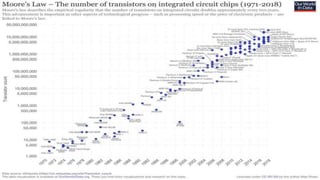


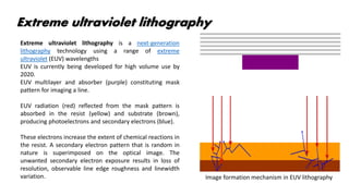


Nanoelectronics refers to using nanotechnology in electronic components to develop nanomachines by scientific methods at the atomic scale. The goal is to reduce the size, risk, and surface area of materials and molecules. Moore's Law predicted that the number of transistors on integrated circuits would double every two years. The semiconductor roadmap assesses requirements to continue Moore's Law by advancing integrated circuit performance and removing roadblocks. Nanolithography techniques like optical lithography, x-ray lithography, and immersion lithography are used in the top-down approach to fabricate leading-edge semiconductors and NEMS through multiple lithographic cycles. The bottom-up approach involves molecular components self-assembling into larger structures from