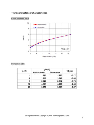
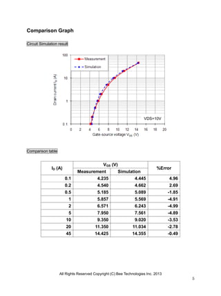
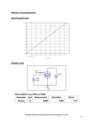
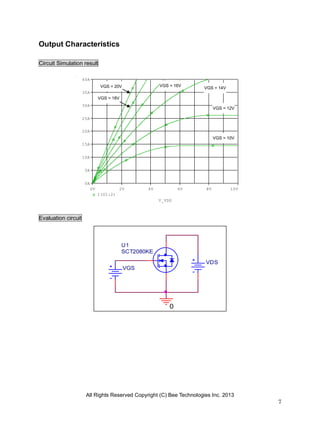
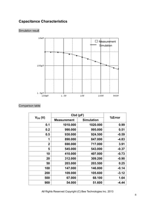
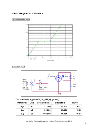
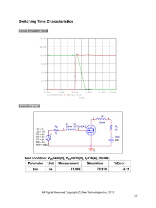
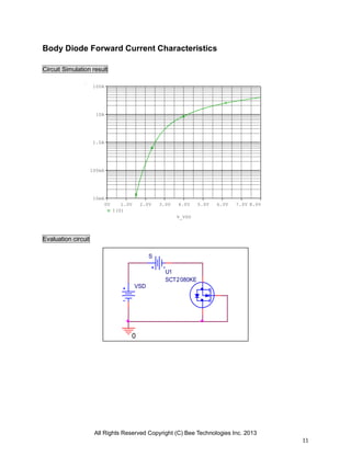
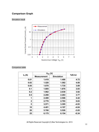
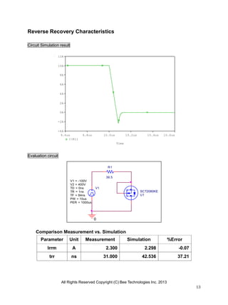
All Rights Reserved Copyright (C) Bee Technologies Inc. 2013
1
Device Modeling Report
Bee Technologies Inc.
COMPONENTS: MOSFET (Model Parameters)
PART NUMBER: SCT2080KE
MANUFACTURER: ROHM
REMARK: Body Diode (Model Parameters)
All Rights Reserved Copyright (C) Bee Technologies Inc. 2013
2
MOSFET MODEL
PSpice model
parameter
Model description
LEVEL
L Channel Length
W Channel Width
KP Transconductance
RS Source Ohmic Resistance
RD Ohmic Drain Resistance
VTO Zero-bias Threshold Voltage
RDS Drain-Source Shunt Resistance
TOX Gate Oxide Thickness
CGSO Zero-bias Gate-Source Capacitance
CGDO Zero-bias Gate-Drain Capacitance
CBD Zero-bias Bulk-Drain Junction Capacitance
MJ Bulk Junction Grading Coefficient
PB Bulk Junction Potential
FC Bulk Junction Forward-bias Capacitance Coefficient
RG Gate Ohmic Resistance
IS Bulk Junction Saturation Current
N Bulk Junction Emission Coefficient
RB Bulk Series Resistance
PHI Surface Inversion Potential
GAMMA Body-effect Parameter
DELTA Width effect on Threshold Voltage
ETA Static Feedback on Threshold Voltage
THETA Mobility Modulation
KAPPA Saturation Field Factor
VMAX Maximum Drift Velocity of Carriers
XJ Metallurgical Junction Depth
UO Surface Mobility
All Rights Reserved Copyright (C) Bee Technologies Inc. 2013
3
Transconductance Characteristics
Circuit Simulation result
Comparison table
ID (A)
gfs (S)
%Error
Measurement Simulation
1 1.273 1.225 -3.77
2 1.817 1.748 -3.80
5 2.920 2.812 -3.70
10 4.161 4.055 -2.55
20 5.919 5.897 -0.37
VDS=10V
All Rights Reserved Copyright (C) Bee Technologies Inc. 2013
4
V_VGS
0V 2V 4V 6V 8V 10V 12V 14V 16V 18V 20V
I(U1:2)
100mA
1.0A
10A
100A
VGS
VDS
10V
0
U1
SCT2080KE
Vgs-Id Characteristics
Circuit Simulation result
Evaluation circuit
All Rights Reserved Copyright (C) Bee Technologies Inc. 2013
5
Comparison Graph
Circuit Simulation result
Comparison table
ID (A)
VGS (V)
%Error
Measurement Simulation
0.1 4.235 4.445 4.96
0.2 4.540 4.662 2.69
0.5 5.185 5.089 -1.85
1 5.857 5.569 -4.91
2 6.571 6.243 -4.99
5 7.950 7.561 -4.89
10 9.350 9.020 -3.53
20 11.350 11.034 -2.78
45 14.425 14.355 -0.49
VDS=10V
All Rights Reserved Copyright (C) Bee Technologies Inc. 2013
6
VGS
18V
0
VDS
U1
SCT2080KE
V_VDS
0V 100mV 200mV 300mV 400mV 500mV 600mV 700mV 800mV
I(U1:2)
0A
1A
2A
3A
4A
5A
6A
7A
8A
9A
10A
Rds(on) Characteristics
Circuit Simulation result
Evaluation circuit
Test condition: VGS=18(V), ID=10(A)
Parameter Unit Measurement Simulation %Error
RDS(on) Ω 0.080 0.084 4.75
All Rights Reserved Copyright (C) Bee Technologies Inc. 2013
7
V_VDS
0V 2V 4V 6V 8V 10V
I(U1:2)
0A
5A
10A
15A
20A
25A
30A
35A
40A
VGS
0
VDS
U1
SCT2080KE
Output Characteristics
Circuit Simulation result
Evaluation circuit
VGS = 10V
VGS = 12V
VGS = 20V
VGS = 18V
VGS = 16V
VGS = 14V
All Rights Reserved Copyright (C) Bee Technologies Inc. 2013
8
Capacitance Characteristics
Simulation result
Comparison table
VDS (V)
Cbd (pF)
%Error
Measurement Simulation
0.1 1010.000 1020.000 0.99
0.2 990.000 995.000 0.51
0.5 930.000 924.500 -0.59
1 890.000 847.000 -4.83
2 690.000 717.000 3.91
5 545.000 543.000 -0.37
10 410.000 407.000 -0.73
20 312.000 309.200 -0.90
50 203.000 203.500 0.25
100 147.000 146.800 -0.14
200 109.000 105.600 -3.12
500 67.000 68.100 1.64
900 54.000 51.600 -4.44
Simulation
Measurement
All Rights Reserved Copyright (C) Bee Technologies Inc. 2013
9
Time*1mA
0 20n 40n 60n 80n 100n 120n
V(W1:3)
0V
5V
10V
15V
20V
D1
dmod
U1
SCT2080KE ID
10A
VDD
400V
0
-
+
W1
ION = 0
IOFF = 1mA
WIGTD = 0
TF = 10n
PW = 10m
PER = 1
I1 = 0
I2 = 1m
TR = 10n
Gate Charge Characteristics
Circuit Simulation result
Evaluation circuit
Test condition: VDD=400(V), VGS=18(V), ID=10(A)
Parameter Unit Measurement Simulation %Error
Qgs nC 27.000 26.856 -0.53
Qgd nC 31.000 31.001 0.00
Qg nC 106.000 84.834 -19.97
All Rights Reserved Copyright (C) Bee Technologies Inc. 2013
10
Time
1.8us 1.9us 2.0us 2.1us 2.2us 2.3us
V(U1:2)/40 V(U1:1)/1.8
0V
2.5V
5.0V
7.5V
10.0V
12.5V
15.0V
L1
30nH
1 2
Rg
1u
U1
SCT2080KE
V1TD = 2u
TF = 4n
PW = 5u
PER = 500u
V1 = 0
TR = 4n
V2 = 18
VDD
400
0
RL
40
L2
50nH
12
Switching Time Characteristics
Circuit Simulation result
Evaluation circuit
Test condition: VDD=400(V), VGS=0/18(V), ID=10(A), RG=0
Parameter Unit Measurement Simulation %Error
ton ns 71.000 70.919 -0.11
All Rights Reserved Copyright (C) Bee Technologies Inc. 2013
11
V_VSD
0V 1.0V 2.0V 3.0V 4.0V 5.0V 6.0V 7.0V 8.0V
I(S)
10mA
100mA
1.0A
10A
100A
0
VSD
U1
SCT2080KE
S
Body Diode Forward Current Characteristics
Circuit Simulation result
Evaluation circuit
All Rights Reserved Copyright (C) Bee Technologies Inc. 2013
12
Comparison Graph
Simulation result
Comparison table
IS (A)
VSD (V)
%Error
Measurement Simulation
0.01 1.419 1.486 4.72
0.02 1.520 1.582 4.08
0.05 1.670 1.735 3.89
0.1 1.805 1.876 3.93
0.2 1.962 2.039 3.92
0.5 2.200 2.283 3.77
1 2.400 2.506 4.42
2 2.770 2.793 0.83
5 3.571 3.395 -4.93
10 4.401 4.197 -4.64
20 5.700 5.526 -3.05
25 6.175 6.154 -0.34
All Rights Reserved Copyright (C) Bee Technologies Inc. 2013
13
Time
9.6us 9.8us 10.0us 10.2us 10.4us 10.6us
I(R1)
-4A
-2A
0A
2A
4A
6A
8A
10A
12A
0
V1TD = 0ns
TF = 84ns
PW = 10us
PER = 1000us
V1 = -100V
TR = 1ns
V2 = 400V
R1
39.5
U1
SCT2080KE
Reverse Recovery Characteristics
Circuit Simulation result
Evaluation circuit
Comparison Measurement vs. Simulation
Parameter Unit Measurement Simulation %Error
Irrm A 2.300 2.298 -0.07
trr ns 31.000 42.536 37.21

SPICE MODEL of SCT2080KE (Standard+BDS Model) in SPICE PARK

  • 1.
    All Rights ReservedCopyright (C) Bee Technologies Inc. 2013 1 Device Modeling Report Bee Technologies Inc. COMPONENTS: MOSFET (Model Parameters) PART NUMBER: SCT2080KE MANUFACTURER: ROHM REMARK: Body Diode (Model Parameters)
  • 2.
    All Rights ReservedCopyright (C) Bee Technologies Inc. 2013 2 MOSFET MODEL PSpice model parameter Model description LEVEL L Channel Length W Channel Width KP Transconductance RS Source Ohmic Resistance RD Ohmic Drain Resistance VTO Zero-bias Threshold Voltage RDS Drain-Source Shunt Resistance TOX Gate Oxide Thickness CGSO Zero-bias Gate-Source Capacitance CGDO Zero-bias Gate-Drain Capacitance CBD Zero-bias Bulk-Drain Junction Capacitance MJ Bulk Junction Grading Coefficient PB Bulk Junction Potential FC Bulk Junction Forward-bias Capacitance Coefficient RG Gate Ohmic Resistance IS Bulk Junction Saturation Current N Bulk Junction Emission Coefficient RB Bulk Series Resistance PHI Surface Inversion Potential GAMMA Body-effect Parameter DELTA Width effect on Threshold Voltage ETA Static Feedback on Threshold Voltage THETA Mobility Modulation KAPPA Saturation Field Factor VMAX Maximum Drift Velocity of Carriers XJ Metallurgical Junction Depth UO Surface Mobility
  • 3.
    All Rights ReservedCopyright (C) Bee Technologies Inc. 2013 3 Transconductance Characteristics Circuit Simulation result Comparison table ID (A) gfs (S) %Error Measurement Simulation 1 1.273 1.225 -3.77 2 1.817 1.748 -3.80 5 2.920 2.812 -3.70 10 4.161 4.055 -2.55 20 5.919 5.897 -0.37 VDS=10V
  • 4.
    All Rights ReservedCopyright (C) Bee Technologies Inc. 2013 4 V_VGS 0V 2V 4V 6V 8V 10V 12V 14V 16V 18V 20V I(U1:2) 100mA 1.0A 10A 100A VGS VDS 10V 0 U1 SCT2080KE Vgs-Id Characteristics Circuit Simulation result Evaluation circuit
  • 5.
    All Rights ReservedCopyright (C) Bee Technologies Inc. 2013 5 Comparison Graph Circuit Simulation result Comparison table ID (A) VGS (V) %Error Measurement Simulation 0.1 4.235 4.445 4.96 0.2 4.540 4.662 2.69 0.5 5.185 5.089 -1.85 1 5.857 5.569 -4.91 2 6.571 6.243 -4.99 5 7.950 7.561 -4.89 10 9.350 9.020 -3.53 20 11.350 11.034 -2.78 45 14.425 14.355 -0.49 VDS=10V
  • 6.
    All Rights ReservedCopyright (C) Bee Technologies Inc. 2013 6 VGS 18V 0 VDS U1 SCT2080KE V_VDS 0V 100mV 200mV 300mV 400mV 500mV 600mV 700mV 800mV I(U1:2) 0A 1A 2A 3A 4A 5A 6A 7A 8A 9A 10A Rds(on) Characteristics Circuit Simulation result Evaluation circuit Test condition: VGS=18(V), ID=10(A) Parameter Unit Measurement Simulation %Error RDS(on) Ω 0.080 0.084 4.75
  • 7.
    All Rights ReservedCopyright (C) Bee Technologies Inc. 2013 7 V_VDS 0V 2V 4V 6V 8V 10V I(U1:2) 0A 5A 10A 15A 20A 25A 30A 35A 40A VGS 0 VDS U1 SCT2080KE Output Characteristics Circuit Simulation result Evaluation circuit VGS = 10V VGS = 12V VGS = 20V VGS = 18V VGS = 16V VGS = 14V
  • 8.
    All Rights ReservedCopyright (C) Bee Technologies Inc. 2013 8 Capacitance Characteristics Simulation result Comparison table VDS (V) Cbd (pF) %Error Measurement Simulation 0.1 1010.000 1020.000 0.99 0.2 990.000 995.000 0.51 0.5 930.000 924.500 -0.59 1 890.000 847.000 -4.83 2 690.000 717.000 3.91 5 545.000 543.000 -0.37 10 410.000 407.000 -0.73 20 312.000 309.200 -0.90 50 203.000 203.500 0.25 100 147.000 146.800 -0.14 200 109.000 105.600 -3.12 500 67.000 68.100 1.64 900 54.000 51.600 -4.44 Simulation Measurement
  • 9.
    All Rights ReservedCopyright (C) Bee Technologies Inc. 2013 9 Time*1mA 0 20n 40n 60n 80n 100n 120n V(W1:3) 0V 5V 10V 15V 20V D1 dmod U1 SCT2080KE ID 10A VDD 400V 0 - + W1 ION = 0 IOFF = 1mA WIGTD = 0 TF = 10n PW = 10m PER = 1 I1 = 0 I2 = 1m TR = 10n Gate Charge Characteristics Circuit Simulation result Evaluation circuit Test condition: VDD=400(V), VGS=18(V), ID=10(A) Parameter Unit Measurement Simulation %Error Qgs nC 27.000 26.856 -0.53 Qgd nC 31.000 31.001 0.00 Qg nC 106.000 84.834 -19.97
  • 10.
    All Rights ReservedCopyright (C) Bee Technologies Inc. 2013 10 Time 1.8us 1.9us 2.0us 2.1us 2.2us 2.3us V(U1:2)/40 V(U1:1)/1.8 0V 2.5V 5.0V 7.5V 10.0V 12.5V 15.0V L1 30nH 1 2 Rg 1u U1 SCT2080KE V1TD = 2u TF = 4n PW = 5u PER = 500u V1 = 0 TR = 4n V2 = 18 VDD 400 0 RL 40 L2 50nH 12 Switching Time Characteristics Circuit Simulation result Evaluation circuit Test condition: VDD=400(V), VGS=0/18(V), ID=10(A), RG=0 Parameter Unit Measurement Simulation %Error ton ns 71.000 70.919 -0.11
  • 11.
    All Rights ReservedCopyright (C) Bee Technologies Inc. 2013 11 V_VSD 0V 1.0V 2.0V 3.0V 4.0V 5.0V 6.0V 7.0V 8.0V I(S) 10mA 100mA 1.0A 10A 100A 0 VSD U1 SCT2080KE S Body Diode Forward Current Characteristics Circuit Simulation result Evaluation circuit
  • 12.
    All Rights ReservedCopyright (C) Bee Technologies Inc. 2013 12 Comparison Graph Simulation result Comparison table IS (A) VSD (V) %Error Measurement Simulation 0.01 1.419 1.486 4.72 0.02 1.520 1.582 4.08 0.05 1.670 1.735 3.89 0.1 1.805 1.876 3.93 0.2 1.962 2.039 3.92 0.5 2.200 2.283 3.77 1 2.400 2.506 4.42 2 2.770 2.793 0.83 5 3.571 3.395 -4.93 10 4.401 4.197 -4.64 20 5.700 5.526 -3.05 25 6.175 6.154 -0.34
  • 13.
    All Rights ReservedCopyright (C) Bee Technologies Inc. 2013 13 Time 9.6us 9.8us 10.0us 10.2us 10.4us 10.6us I(R1) -4A -2A 0A 2A 4A 6A 8A 10A 12A 0 V1TD = 0ns TF = 84ns PW = 10us PER = 1000us V1 = -100V TR = 1ns V2 = 400V R1 39.5 U1 SCT2080KE Reverse Recovery Characteristics Circuit Simulation result Evaluation circuit Comparison Measurement vs. Simulation Parameter Unit Measurement Simulation %Error Irrm A 2.300 2.298 -0.07 trr ns 31.000 42.536 37.21