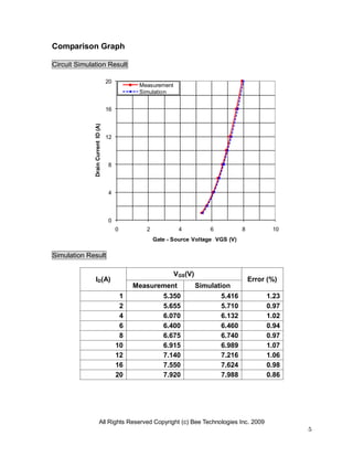
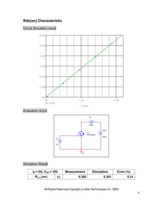
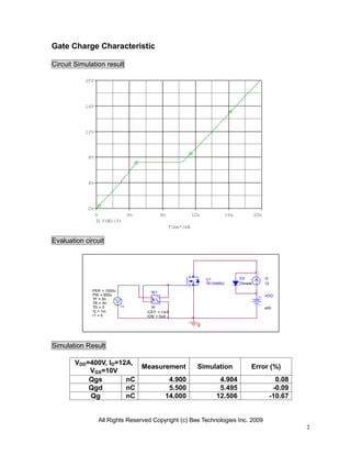
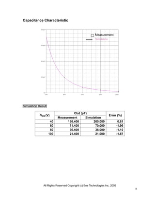
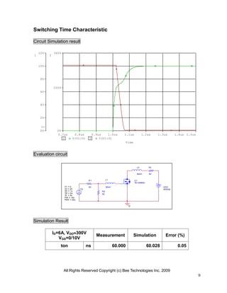
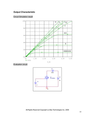
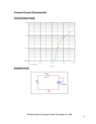
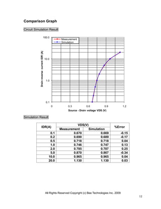
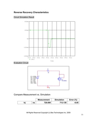
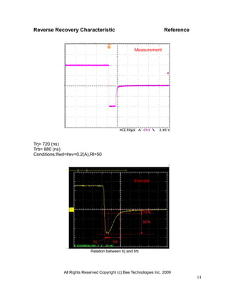
All Rights Reserved Copyright (c) Bee Technologies Inc. 2009
1
Device Modeling Report
Bee Technologies Inc.
COMPONENTS: MOSFET (Model Parameters)
PART NUMBER: TK12A60U
MANUFACTURER: TOSHIBA
REMARK: Body Diode (Model Parameters)
All Rights Reserved Copyright (c) Bee Technologies Inc. 2009
2
MOSFET MODEL
PSpice model
parameter
Model description
LEVEL
L Channel Length
W Channel Width
KP Transconductance
RS Source Ohmic Resistance
RD Ohmic Drain Resistance
VTO Zero-bias Threshold Voltage
RDS Drain-Source Shunt Resistance
TOX Gate Oxide Thickness
CGSO Zero-bias Gate-Source Capacitance
CGDO Zero-bias Gate-Drain Capacitance
CBD Zero-bias Bulk-Drain Junction Capacitance
MJ Bulk Junction Grading Coefficient
PB Bulk Junction Potential
FC Bulk Junction Forward-bias Capacitance Coefficient
RG Gate Ohmic Resistance
IS Bulk Junction Saturation Current
N Bulk Junction Emission Coefficient
RB Bulk Series Resistance
PHI Surface Inversion Potential
GAMMA Body-effect Parameter
DELTA Width effect on Threshold Voltage
ETA Static Feedback on Threshold Voltage
THETA Mobility Modulation
KAPPA Saturation Field Factor
VMAX Maximum Drift Velocity of Carriers
XJ Metallurgical Junction Depth
UO Surface Mobility
All Rights Reserved Copyright (c) Bee Technologies Inc. 2009
3
0
2
4
6
8
10
0 2 4 6 8 10
gfs(S)
Drain Current ID (A)
Measurement
Simulation
Transconductance Characteristic
Circuit Simulation Result
Comparison table
Id(A)
gfs (s)
Error (%)
Measurement Simulation
1.0 2.750 2.832 2.982
2.0 3.900 3.958 1.487
5.0 6.050 6.118 1.124
10.0 8.400 8.439 0.464
All Rights Reserved Copyright (c) Bee Technologies Inc. 2009
4
V1
0Vdc
V2
20
0
V3
0Vdc
U1
TK12A60U
V_V1
0V 2V 4V 6V 8V 10V
I(V3)
0A
4A
8A
12A
16A
20A
Vgs-Id Characteristic
Circuit Simulation result
Evaluation circuit
All Rights Reserved Copyright (c) Bee Technologies Inc. 2009
5
0
4
8
12
16
20
0 2 4 6 8 10
DrainCurrentID(A)
Gate - Source Voltage VGS (V)
Measurement
Simulation
Comparison Graph
Circuit Simulation Result
Simulation Result
ID(A)
VGS(V)
Error (%)
Measurement Simulation
1 5.350 5.416 1.23
2 5.655 5.710 0.97
4 6.070 6.132 1.02
6 6.400 6.460 0.94
8 6.675 6.740 0.97
10 6.915 6.989 1.07
12 7.140 7.216 1.06
16 7.550 7.624 0.98
20 7.920 7.988 0.86
All Rights Reserved Copyright (c) Bee Technologies Inc. 2009
6
0
V3
0Vdc
VDS
0Vdc
V1
10
U1
TK12A60U
V_VDS
0V 1.0V 2.0V
I(V3)
0A
1.0A
2.0A
3.0A
4.0A
5.0A
6.0A
Rds(on) Characteristic
Circuit Simulation result
Evaluation circuit
Simulation Result
ID = 6A, VGS = 10V Measurement Simulation Error (%)
RDS (on)  0.360 0.361 0.31
All Rights Reserved Copyright (c) Bee Technologies Inc. 2009
7
I1TD = 0
TF = 5n
PW = 600u
PER = 1000u
I1 = 0
I2 = 1m
TR = 5n
VDD
400
-
+
W1
ION = 0uA
IOFF = 1mA
W
I2
12
0
D2
Dbreak
U1
TK12A60U
Time*1mA
0 4n 8n 12n 16n 20n
V(W1:3)
0V
4V
8V
12V
16V
20V
Gate Charge Characteristic
Circuit Simulation result
Evaluation circuit
Simulation Result
VDD=400V, ID=12A,
VGS=10V
Measurement Simulation Error (%)
Qgs nC 4.900 4.904 0.08
Qgd nC 5.500 5.495 -0.09
Qg nC 14.000 12.506 -10.67
All Rights Reserved Copyright (c) Bee Technologies Inc. 2009
8
Capacitance Characteristic
Simulation Result
VDS (V)
Cbd (pF)
Error (%)
Measurement Simulation
40 198.400 200.000 0.81
60 71.400 70.000 -1.96
80 36.400 36.000 -1.10
100 21.400 21.000 -1.87
Simulation
Measurement
All Rights Reserved Copyright (c) Bee Technologies Inc. 2009
9
Time
0.7us 0.8us 0.9us 1.0us 1.1us 1.2us 1.3us 1.4us 1.5us
1 V(U1:G) 2 V(U1:D)
0V
2V
4V
6V
8V
10V
12V
1
>>
0V
200V
360V
2
0
VDD
303VdcV2
TD = 1u
TF = 5n
PW = 10u
PER = 20u
V1 = 0
TR = 5n
V2 = 20
U1
TK12A60U
L2
50nH
R2
50
R1
50
L1
30nH
RL
50
Switching Time Characteristic
Circuit Simulation result
Evaluation circuit
Simulation Result
ID=6A, VDD300V
VGS=0/10V
Measurement Simulation Error (%)
ton ns 60.000 60.028 0.05
All Rights Reserved Copyright (c) Bee Technologies Inc. 2009
10
V2
50
V1
0
0
V3
0Vdc
U1
TK12A60U
V_V2
0V 1.0V 2.0V 3.0V 4.0V 5.0V
I(V3)
0A
2A
4A
6A
8A
10A
Output Characteristic
Circuit Simulation result
Evaluation circuit
VGS=5.5V
7.5
6
10 8
7
6.5
All Rights Reserved Copyright (c) Bee Technologies Inc. 2009
11
U1
TK12A60U
VDS
0
Vsense
0Vdc
V_VDS
0V 0.3V 0.6V 0.9V 1.2V
I(Vsense)
100mA
1.0A
10A
100A
Forward Current Characteristic
Circuit Simulation Result
Evaluation Circuit
All Rights Reserved Copyright (c) Bee Technologies Inc. 2009
12
0.1
1.0
10.0
100.0
0 0.3 0.6 0.9 1.2
DrainreversecurrentIDR(A)
Source - Drain voltage VDS (V)
Measurement
Simulation
Comparison Graph
Circuit Simulation Result
Simulation Result
IDR(A)
VDS(V)
%Error
Measurement Simulation
0.1 0.670 0.669 -0.15
0.2 0.690 0.689 -0.17
0.5 0.718 0.718 0.04
1.0 0.746 0.747 0.13
2.0 0.785 0.787 0.25
5.0 0.870 0.867 -0.34
10.0 0.965 0.965 0.04
20.0 1.130 1.130 0.03
All Rights Reserved Copyright (c) Bee Technologies Inc. 2009
13
V1
TD = 0.5us
TF = 10ns
PW = 20us
PER = 50us
V1 = -9.45v
TR = 10ns
V2 = 10.65v
0
R1
50
U1
TK12A60U
Time
12us 14us 16us 18us 20us 22us 24us 26us 28us 30us
I(R1)
-400mA
-200mA
0A
200mA
400mA
Reverse Recovery Characteristics
Circuit Simulation Result
Evaluation Circuit
Compare Measurement vs. Simulation
Measurement Simulation Error (%)
trj ns 720.000 713.130 -0.95
All Rights Reserved Copyright (c) Bee Technologies Inc. 2009
14
Reverse Recovery Characteristic Reference
Trj= 720 (ns)
Trb= 880 (ns)
Conditions:Ifwd=lrev=0.2(A),Rl=50
Relation between trj and trb
Example
Measurement

SPICE MODEL of TK12A60U (Standard+BDS Model) in SPICE PARK

  • 1.
    All Rights ReservedCopyright (c) Bee Technologies Inc. 2009 1 Device Modeling Report Bee Technologies Inc. COMPONENTS: MOSFET (Model Parameters) PART NUMBER: TK12A60U MANUFACTURER: TOSHIBA REMARK: Body Diode (Model Parameters)
  • 2.
    All Rights ReservedCopyright (c) Bee Technologies Inc. 2009 2 MOSFET MODEL PSpice model parameter Model description LEVEL L Channel Length W Channel Width KP Transconductance RS Source Ohmic Resistance RD Ohmic Drain Resistance VTO Zero-bias Threshold Voltage RDS Drain-Source Shunt Resistance TOX Gate Oxide Thickness CGSO Zero-bias Gate-Source Capacitance CGDO Zero-bias Gate-Drain Capacitance CBD Zero-bias Bulk-Drain Junction Capacitance MJ Bulk Junction Grading Coefficient PB Bulk Junction Potential FC Bulk Junction Forward-bias Capacitance Coefficient RG Gate Ohmic Resistance IS Bulk Junction Saturation Current N Bulk Junction Emission Coefficient RB Bulk Series Resistance PHI Surface Inversion Potential GAMMA Body-effect Parameter DELTA Width effect on Threshold Voltage ETA Static Feedback on Threshold Voltage THETA Mobility Modulation KAPPA Saturation Field Factor VMAX Maximum Drift Velocity of Carriers XJ Metallurgical Junction Depth UO Surface Mobility
  • 3.
    All Rights ReservedCopyright (c) Bee Technologies Inc. 2009 3 0 2 4 6 8 10 0 2 4 6 8 10 gfs(S) Drain Current ID (A) Measurement Simulation Transconductance Characteristic Circuit Simulation Result Comparison table Id(A) gfs (s) Error (%) Measurement Simulation 1.0 2.750 2.832 2.982 2.0 3.900 3.958 1.487 5.0 6.050 6.118 1.124 10.0 8.400 8.439 0.464
  • 4.
    All Rights ReservedCopyright (c) Bee Technologies Inc. 2009 4 V1 0Vdc V2 20 0 V3 0Vdc U1 TK12A60U V_V1 0V 2V 4V 6V 8V 10V I(V3) 0A 4A 8A 12A 16A 20A Vgs-Id Characteristic Circuit Simulation result Evaluation circuit
  • 5.
    All Rights ReservedCopyright (c) Bee Technologies Inc. 2009 5 0 4 8 12 16 20 0 2 4 6 8 10 DrainCurrentID(A) Gate - Source Voltage VGS (V) Measurement Simulation Comparison Graph Circuit Simulation Result Simulation Result ID(A) VGS(V) Error (%) Measurement Simulation 1 5.350 5.416 1.23 2 5.655 5.710 0.97 4 6.070 6.132 1.02 6 6.400 6.460 0.94 8 6.675 6.740 0.97 10 6.915 6.989 1.07 12 7.140 7.216 1.06 16 7.550 7.624 0.98 20 7.920 7.988 0.86
  • 6.
    All Rights ReservedCopyright (c) Bee Technologies Inc. 2009 6 0 V3 0Vdc VDS 0Vdc V1 10 U1 TK12A60U V_VDS 0V 1.0V 2.0V I(V3) 0A 1.0A 2.0A 3.0A 4.0A 5.0A 6.0A Rds(on) Characteristic Circuit Simulation result Evaluation circuit Simulation Result ID = 6A, VGS = 10V Measurement Simulation Error (%) RDS (on)  0.360 0.361 0.31
  • 7.
    All Rights ReservedCopyright (c) Bee Technologies Inc. 2009 7 I1TD = 0 TF = 5n PW = 600u PER = 1000u I1 = 0 I2 = 1m TR = 5n VDD 400 - + W1 ION = 0uA IOFF = 1mA W I2 12 0 D2 Dbreak U1 TK12A60U Time*1mA 0 4n 8n 12n 16n 20n V(W1:3) 0V 4V 8V 12V 16V 20V Gate Charge Characteristic Circuit Simulation result Evaluation circuit Simulation Result VDD=400V, ID=12A, VGS=10V Measurement Simulation Error (%) Qgs nC 4.900 4.904 0.08 Qgd nC 5.500 5.495 -0.09 Qg nC 14.000 12.506 -10.67
  • 8.
    All Rights ReservedCopyright (c) Bee Technologies Inc. 2009 8 Capacitance Characteristic Simulation Result VDS (V) Cbd (pF) Error (%) Measurement Simulation 40 198.400 200.000 0.81 60 71.400 70.000 -1.96 80 36.400 36.000 -1.10 100 21.400 21.000 -1.87 Simulation Measurement
  • 9.
    All Rights ReservedCopyright (c) Bee Technologies Inc. 2009 9 Time 0.7us 0.8us 0.9us 1.0us 1.1us 1.2us 1.3us 1.4us 1.5us 1 V(U1:G) 2 V(U1:D) 0V 2V 4V 6V 8V 10V 12V 1 >> 0V 200V 360V 2 0 VDD 303VdcV2 TD = 1u TF = 5n PW = 10u PER = 20u V1 = 0 TR = 5n V2 = 20 U1 TK12A60U L2 50nH R2 50 R1 50 L1 30nH RL 50 Switching Time Characteristic Circuit Simulation result Evaluation circuit Simulation Result ID=6A, VDD300V VGS=0/10V Measurement Simulation Error (%) ton ns 60.000 60.028 0.05
  • 10.
    All Rights ReservedCopyright (c) Bee Technologies Inc. 2009 10 V2 50 V1 0 0 V3 0Vdc U1 TK12A60U V_V2 0V 1.0V 2.0V 3.0V 4.0V 5.0V I(V3) 0A 2A 4A 6A 8A 10A Output Characteristic Circuit Simulation result Evaluation circuit VGS=5.5V 7.5 6 10 8 7 6.5
  • 11.
    All Rights ReservedCopyright (c) Bee Technologies Inc. 2009 11 U1 TK12A60U VDS 0 Vsense 0Vdc V_VDS 0V 0.3V 0.6V 0.9V 1.2V I(Vsense) 100mA 1.0A 10A 100A Forward Current Characteristic Circuit Simulation Result Evaluation Circuit
  • 12.
    All Rights ReservedCopyright (c) Bee Technologies Inc. 2009 12 0.1 1.0 10.0 100.0 0 0.3 0.6 0.9 1.2 DrainreversecurrentIDR(A) Source - Drain voltage VDS (V) Measurement Simulation Comparison Graph Circuit Simulation Result Simulation Result IDR(A) VDS(V) %Error Measurement Simulation 0.1 0.670 0.669 -0.15 0.2 0.690 0.689 -0.17 0.5 0.718 0.718 0.04 1.0 0.746 0.747 0.13 2.0 0.785 0.787 0.25 5.0 0.870 0.867 -0.34 10.0 0.965 0.965 0.04 20.0 1.130 1.130 0.03
  • 13.
    All Rights ReservedCopyright (c) Bee Technologies Inc. 2009 13 V1 TD = 0.5us TF = 10ns PW = 20us PER = 50us V1 = -9.45v TR = 10ns V2 = 10.65v 0 R1 50 U1 TK12A60U Time 12us 14us 16us 18us 20us 22us 24us 26us 28us 30us I(R1) -400mA -200mA 0A 200mA 400mA Reverse Recovery Characteristics Circuit Simulation Result Evaluation Circuit Compare Measurement vs. Simulation Measurement Simulation Error (%) trj ns 720.000 713.130 -0.95
  • 14.
    All Rights ReservedCopyright (c) Bee Technologies Inc. 2009 14 Reverse Recovery Characteristic Reference Trj= 720 (ns) Trb= 880 (ns) Conditions:Ifwd=lrev=0.2(A),Rl=50 Relation between trj and trb Example Measurement