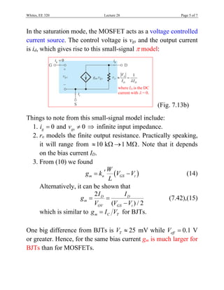
The document discusses the use of MOSFETs as small-signal amplifiers and introduces a conceptual MOSFET amplifier model. It highlights the importance of biasing the MOSFET in the saturation region and the resulting linear operation conditions, including the definition and relevance of transconductance. Additionally, the document contrasts MOSFETs with BJTs, noting advantages such as higher input resistance and lower power dissipation.

![Whites, EE 320 Lecture 28 Page 3 of 7
If this small-signal condition (7) is satisfied, then from (6) the
total drain current is approximately the linear summation
DC AC
D D di I i (7.31),(8)
where d n GS t gs
W
i k V V v
L
. (9)
From this expression (9) we see that the AC drain current id is
related to vgs by the so-called transistor transconductance, gm:
d
m n GS t
gs
i W
g k V V
v L
[S] (7.32),(10)
which is sometimes expressed in terms of the overdrive voltage
OV GS tV V V
m n OV
W
g k V
L
[S] (7.33),(11)
Because of the VGS term in (10) and (11), this gm depends on the
bias, which is just like a BJT.
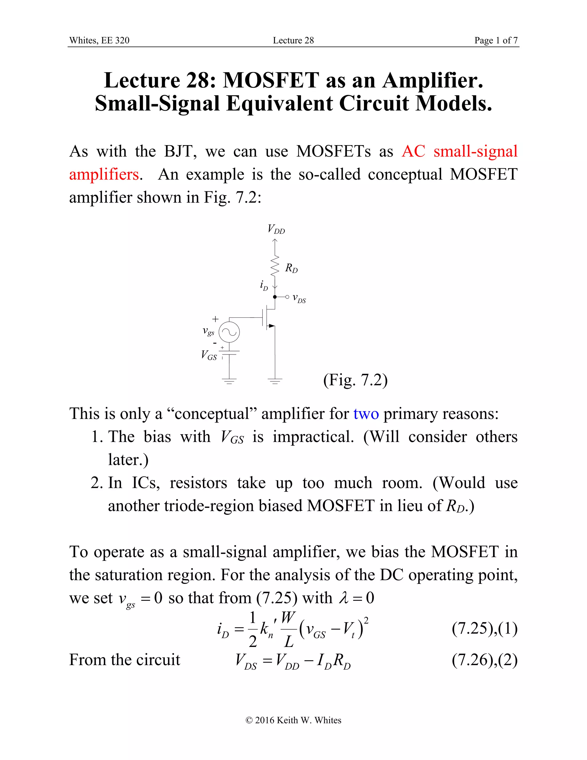
Physically, this transconductance gm equals the slope of the iD-
vGS characteristic curve at the Q point:
GS GS
D
m
GS v V
i
g
v
(7.34),(12)](https://image.slidesharecdn.com/320lecture28-180717101746/85/MOSFET-as-an-Amplifier-3-320.jpg)
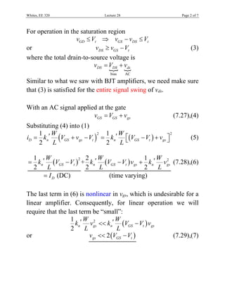
![Whites, EE 320 Lecture 28 Page 4 of 7
(Fig. 7.11)
Lastly, it can be easily show that for this conceptual amplifier in
Fig. 7.2,
ds
v m D
gs
v
A g R
v
(7.36),(13)
Consequently, v mA g , which is the same result we found for a
similar BJT conceptual amplifier [see (7.78)].
MOSFET Small-Signal Equivalent Models
For circuit analysis, it is convenient to use equivalent small-
signal models for MOSFETs – as it was with BJTs.](https://image.slidesharecdn.com/320lecture28-180717101746/85/MOSFET-as-an-Amplifier-4-320.jpg)