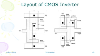
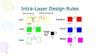
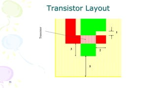
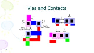
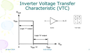
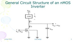
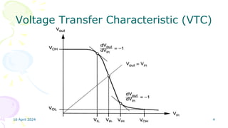
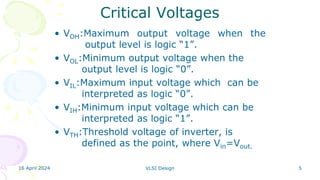
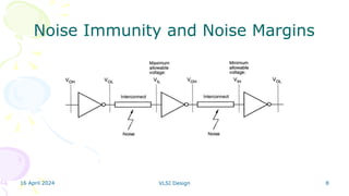
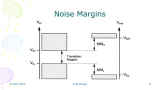
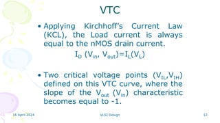
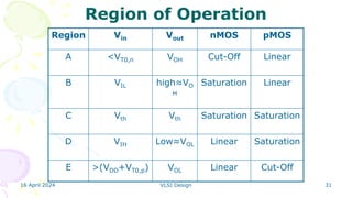
The document discusses the analysis and design of CMOS inverters. It covers topics like the voltage transfer characteristic (VTC) of inverters implemented using nMOS, depletion-nMOS, and CMOS load configurations. It derives the expressions for critical voltages like VOH, VOL, VIL, VIH, Vth for each case. Noise margins and their importance for noise immunity is explained. Layout design considerations for CMOS inverters including design rules and layers are also covered. Examples of numerical calculations related to the topics are presented.


![16 April 2024 VLSI Design 14
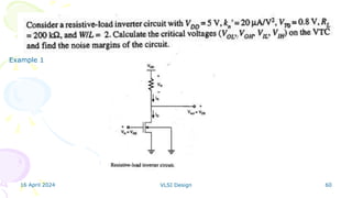
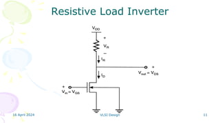
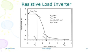
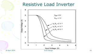
Resistive Load Inverter
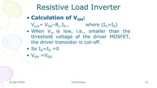
• Calculation of VOL:
• IR= IDLinear
• (VDD-VOUT)/RL= Kn/2[2(VDD-VTO).VOL- VOL
2]](https://image.slidesharecdn.com/invertersupdated-240416132528-081473cd/85/inveatedpresentationwhich-has-the-details-pptx-14-320.jpg)
![16 April 2024 VLSI Design 15
Resistive Load Inverter
• Calculation of VIL:
• IR= IDSaturation
• (VDD-VOUT)/RL= Kn/2[(Vin-VTO)2]](https://image.slidesharecdn.com/invertersupdated-240416132528-081473cd/85/inveatedpresentationwhich-has-the-details-pptx-15-320.jpg)
![16 April 2024 VLSI Design 16
Resistive Load Inverter
• Calculation of VIH:
• IR= IDLinear
• (VDD-Vout)/RL= Kn/2[(Vin-VTO).Vout-Vout
2]
• Differenting both sides w.r.t Vin and
substituting the slope=-1](https://image.slidesharecdn.com/invertersupdated-240416132528-081473cd/85/inveatedpresentationwhich-has-the-details-pptx-16-320.jpg)
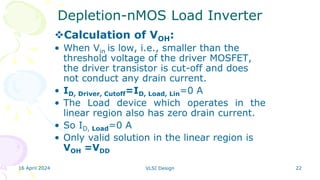
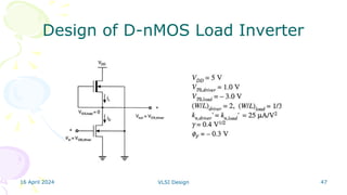
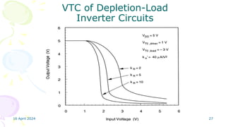
![16 April 2024 VLSI Design 23
Depletion-nMOS Load Inverter
Calculation of VOL:
• ID, Driver, Lin = ID, Load, Sat
• ID, Driver, Lin =(Kdriver/2)[2(VOH-VTO).VOL- VOL
2]
• ID, Load, Sat =(KLoad/2)[-VT, Load (VOL)]2](https://image.slidesharecdn.com/invertersupdated-240416132528-081473cd/85/inveatedpresentationwhich-has-the-details-pptx-23-320.jpg)
![16 April 2024 VLSI Design 24
Depletion-nMOS Load Inverter
Calculation of VIL:
• ID, Driver, Sat = ID, Load, Lin
• ID, Driver, Sat =(KDriver/2)[Vin-VTO]2
• ID, Load, Sat =(KLoad/2){2[VT, Load (Vout)](VDD-
Vout)- (VDD-Vout)2}
• Differenting both sides w.r.t Vin and
substituting the slope=-1](https://image.slidesharecdn.com/invertersupdated-240416132528-081473cd/85/inveatedpresentationwhich-has-the-details-pptx-24-320.jpg)
![16 April 2024 VLSI Design 25
Depletion-nMOS Load Inverter
Calculation of VIH:
• ID, Driver, Lin = ID, Load, Sat
• ID, Driver, Lin =(KDriver/2)[2(Vin-VTO) Vout-
Vout
2]
• ID, Load, Sat =(KLoad/2)[-VT, Load (Vout)]2
• Differenting both sides w.r.t Vin and
substituting the slope=-1](https://image.slidesharecdn.com/invertersupdated-240416132528-081473cd/85/inveatedpresentationwhich-has-the-details-pptx-25-320.jpg)
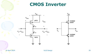
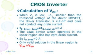
![16 April 2024 VLSI Design 33
CMOS Inverter
Calculation of VOL:
• ID, Driver, Lin = ID, Load, Cut-off
• ID, Driver, Lin =(Kdriver/2)[2(VDD-VTO).VOL- VOL
2]
• ID, Load, Cut-off =0A
• VOL =0 V](https://image.slidesharecdn.com/invertersupdated-240416132528-081473cd/85/inveatedpresentationwhich-has-the-details-pptx-33-320.jpg)
![16 April 2024 VLSI Design 34
CMOS Inverter
Calculation of VIL:
• ID, nMOS, Sat = ID, pMOS, Lin
• ID, nMOS, Sat=(Kn/2)[VGS,n-VTO,n]2
• ID, pMOS, Lin=(KP/2)[2(VGS,p-VTO,p)VDS,p-VDS,p)2]
• Differenting both sides w.r.t Vin and
substituting the slope=-1
• VIL=(2Vout + VTO,p- VDD+ KRVTO,n)/(1+KR)
• Transconductance Ratio(KR)
• KR = Kn/KP](https://image.slidesharecdn.com/invertersupdated-240416132528-081473cd/85/inveatedpresentationwhich-has-the-details-pptx-34-320.jpg)
![16 April 2024 VLSI Design 35
CMOS Inverter
Calculation of VIH:
• ID, Driver, Lin= ID, Load, Sat
• ID, nMOS, Lin= (Kn/2)[2(VGS,n-VTO,n)VDS,n-VDS,n)2]
• ID, pMOS, Sat=(Kp/2)[VGS,p-VTO,p]2
• Differenting both sides w.r.t Vin and
substituting the slope=-1
• VIH=(VDD+VTO,p+KR (2Vout+VTO,n))/(1+KR)
• Transconductance Ratio(KR)
• KR = Kn/KP](https://image.slidesharecdn.com/invertersupdated-240416132528-081473cd/85/inveatedpresentationwhich-has-the-details-pptx-35-320.jpg)
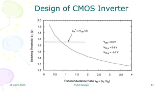
![16 April 2024 VLSI Design 36
CMOS Inverter
Calculation of Vth:
• ID, Driver, Sat= ID, Load, Sat
• ID, nMOS, Sat= (Kn/2)(VGS,n-VTO,n)2
• ID, pMOS, Sat=(Kp/2)[VGS,p-VTO,p]2
• Vth=VTO,n+KR
-1/2(VDD+VTO,p)/(1+KR
-1/2)
• Transconductance Ratio(KR)
• KR=Kn/KP](https://image.slidesharecdn.com/invertersupdated-240416132528-081473cd/85/inveatedpresentationwhich-has-the-details-pptx-36-320.jpg)