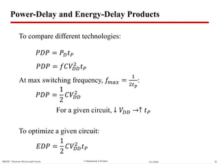
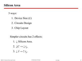
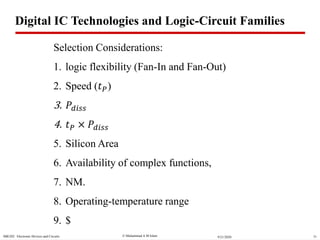
Download to read offline


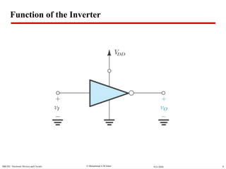
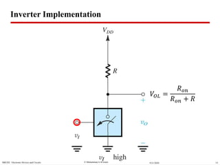
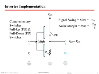
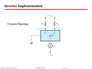
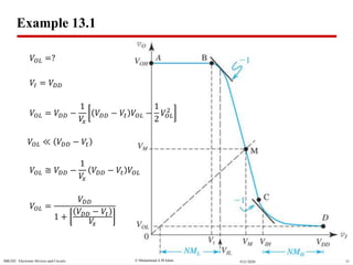
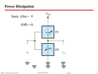
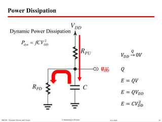
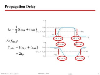
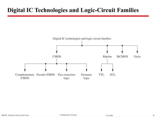
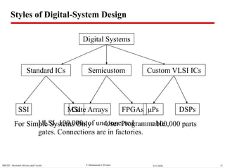

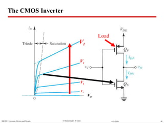
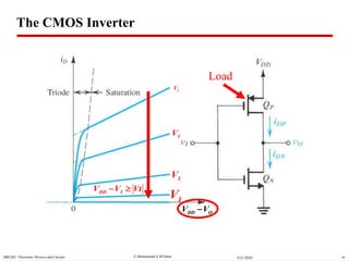
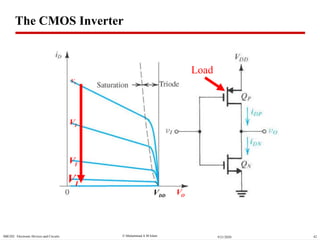
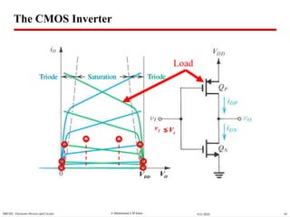
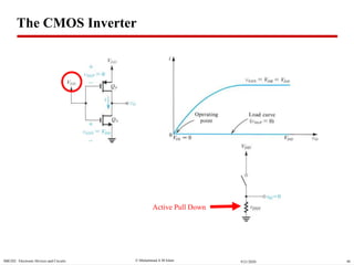
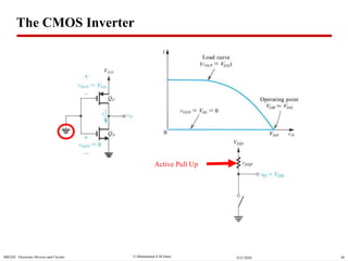
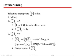
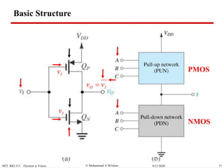
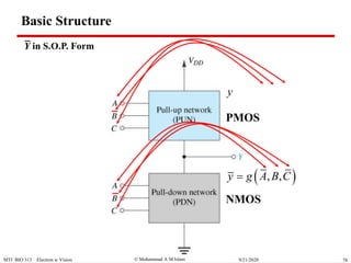
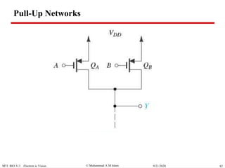
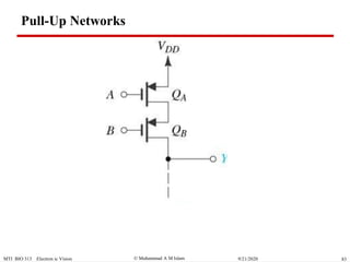
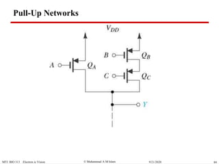
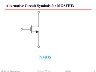
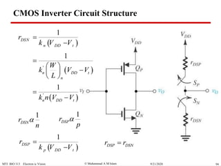

This document discusses CMOS digital logic circuits. It covers special characteristics like fan-out, power dissipation, and propagation delay. It then describes the basic CMOS inverter circuit. The inverter uses complementary NMOS and PMOS transistors for the pull-down and pull-up networks. When the input is low, the NMOS transistor is on and the PMOS is off, pulling the output high. When the input is high, the opposite occurs. This allows the output to switch between 0V and the supply voltage with very low static power dissipation.


