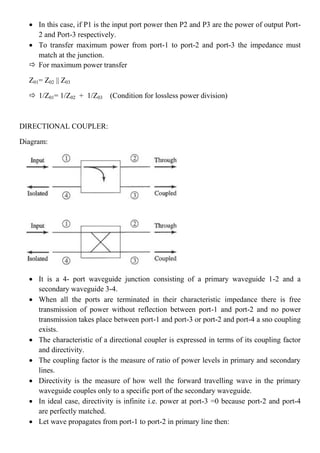
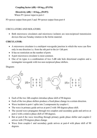
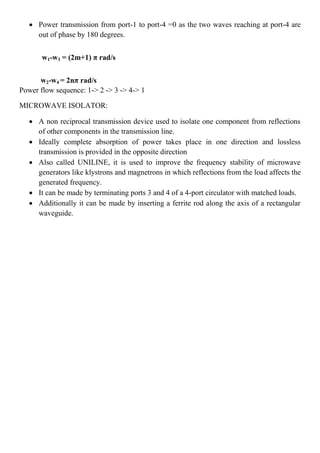
Downloaded 121 times

![In equation ① & ②
V= V(z, t)= Re{Vs(z)ejὠt
}
I= I(z, t)= Re{Is(z)ejὠt
}
Putting V & I in equation ①
-d V/dz= R I + L d I/dt
-d [Re{Vs(z)ejὠt
}]/dz= R [Re{Is(z)ejὠt
}] + L d [Re{Is(z)ejὠt
}]/dt
- Re{d Vs(z)ejὠt
/dz}= R Is(z) [Re{ ejὠt
}] + L [Re{j ὠ Is(z)ejὠt
}]
-d Vs(z)/dz= (R + jὠL)Is(z) -------------③
Similarly,
-d Is(z)/dz= (G + jὠC)Vs(z) -------------④
Equation ③ & ④ are called Telegraphers Equation or low frequency equation.
The transmission line discussed so far were of lossy type in which the conductors comprising
the line are imperfect ( c )and the dielectric in which the conductors are embedded is
lossy ( 0c ).
Having considered this general case , we may now consider two special cases:
1. Lossless line(R=0=G)
2. Distortionless line(R/l=G/c)
Case-1:Lossless line(R=0=G):- The transmission line is said to be lossless if the
conductors of the line are perfect c and the dielectric separating between them is
lossless( 0c ).
For such a line R=0=G .This is the necessary condition for a line to be lossless.
Hence for this line the attenuation constant α=0. But the propagation constant
γ=√(R+j⍵L)(G+ j⍵C)
But we also know that γ=α+jβ.
so on solving we get:-
√{(RG +R j⍵C +G j⍵L+j2
⍵2
LC=jβ (∵α=0)](https://image.slidesharecdn.com/microwaveengineering-160418161558/85/Microwave-Engineering-Lecture-Notes-6-320.jpg)
![So we get √(j2
⍵2
LC)=jβ
this shows that the phase constant β= ⍵√LC and for the characteristic impedance
Z0=√{(R+j⍵L)/(G+ j⍵C)}
so Z0= √(L/C)
and the phase velocity vp=⍵/β=1/√(LC)=fλ
Case-2:Distortionless Line(R/L=G/C):- A distortionless line is the one in which the
attenuation constant α is frequency independent while the phase constant β is linearly
dependent on frequency.
From the expression for α and β a distortionless line results if the parameters are such:-
R/L=G/C
So γ=√( R+j⍵L)(G+ j⍵C)
Hence γ=√RG(1+j⍵L/R)(1+j⍵C/G)
=√RG(1+ j⍵C/G)2
=α+jβ
so α= √RG and β=⍵√LC
The above values shows that α is not dependent on frequency and β is a linearly
dependent on frequency.
Also characteristic impedance=Z0=√(R+j⍵L)/(G+ j⍵C)
Z0=√[R(1+j⍵L/R)]/[G(1+j⍵C/G)]
Z0=√R/G=√L/C
Also the phase velocity vp=⍵/β=1/√LC=fλ
Or λ=1/f√LC
Microwave Line:- A microwave line is the one where the parameters are such :-R<<⍵L
and G<<⍵C
So the characteristic impedance Z0=√(R+j⍵L)/(G+ j⍵C)
So substituting the parameters we get:- Z0=√L/C
And propagation constant γ=√( R+j⍵L)(G+ j⍵C)
So γ=√j⍵L(1+R/j⍵L) j⍵c(1+G/j⍵C)
=j⍵√LC[(1+R/j⍵L)1/2
(1+G/j⍵C)1/2](https://image.slidesharecdn.com/microwaveengineering-160418161558/85/Microwave-Engineering-Lecture-Notes-7-320.jpg)
![=j⍵√LC(1+R/2j⍵L)(1+G/2j⍵L)
=j⍵√LC [1+R/2j⍵L+G/2j⍵C]
γ =j⍵√LC+ (R/2)(√C/L) + G√L/C
but we also know that γ=α+jβ
so we have α=(R/2)(√C/L) and β=j⍵√LC
and the phase velocity vp=⍵/β=2Π/(j⍵√LC)
so vp= 2Π/(j2Πf√LC
hence vp= 1/(jf√LC)
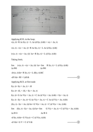
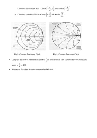
SMITH CHART
For evaluating the rectangular components, or the magnitude and phase of an input
impedance or admittance, voltage, current, and related transmission functions at all points
along a transmission line, including:
• Complex voltage and current reflections coefficients
• Complex voltage and current transmission coefficents
• Power reflection and transmission coefficients
• Reflection Loss
• Return Loss
• Standing Wave Loss Factor
• Maximum and minimum of voltage and current, and SWR
• Shape, position, and phase distribution along voltage and current standing waves
• Evaluating effects of shunt and series impedances on the impedance of a transmission line.
• For displaying and evaluating the input impedance characteristics of resonant and anti-
resonant stubs including the bandwidth and Q.
• Designing impedance matching networks using single or multiple open or shorted stubs.
• Designing impedance matching networks using quarter wave line sections.
• Designing impedance matching networks using lumped L-C components.
• For displaying complex impedances verses frequency.
• For displaying s-parameters of a network verses frequency.](https://image.slidesharecdn.com/microwaveengineering-160418161558/85/Microwave-Engineering-Lecture-Notes-8-320.jpg)
![WAVEGUIDE
The transmission line can’t propagate high range of frequencies in GHz due to skin effect.
Waveguides are generally used to propagate microwave signal and they always operate
beyond certain frequency that is called “cut off frequency”. so they behaves as high pass
filter.
SKIN EFFECT :xc=
1
(2∗𝜋∗𝑓∗𝑐)
According to this relation,as frequency increases, xc tends to zero, that is short circuit. Hence
signal becomes grounded and can’t propagate further which is called skin effect.
Types of waveguides: - (1)rectangular waveguide (2)cylindrical waveguide (3)elliptical
waveguide (4)parallel waveguide
RECTANGULAR WAVEGUIDE :
Let us assume that the wave is travelling along z-axis and field variation along z-direction is
equal to e-Ƴz
,where z=direction of propagation and Ƴ= propagation constant.
Assume the waveguide is lossless (α=0) and walls are perfect conductor (σ=∞). According to
maxwell’s equation: ∇ × H=J+𝜕𝐷/𝜕𝑡 and ∇ × E = -𝜕𝐵/𝜕𝑡 .
So ∇ × H=J𝜔 ∈ 𝐸 − − − (1. 𝑎) , ∇ × E = −J𝜔𝜇𝐻. ---------(1.b)
Expanding equation (1),
|
𝐴𝑥 𝐴𝑦 𝐴𝑧
𝜕/𝜕𝑥 𝜕/𝜕𝑦 𝜕/𝜕𝑧
𝐻𝑥 𝐻𝑦 𝐻𝑧
|= J𝜔 ∈ [𝐸𝑥𝐴𝑥 + 𝐸𝑦𝐴𝑦 + 𝐸𝑧𝐴𝑧]
By equating coefficients of both sides we get,
𝜕
𝜕𝑦
𝐻𝑧 −
𝜕
𝜕𝑧
𝐻𝑦 =J𝜔 ∈Ex -----------------2(a)
−
𝜕
𝜕𝑥
𝐻𝑧 +
𝜕
𝜕𝑧
𝐻𝑥 = J𝜔 ∈ 𝐸𝑦 -----------2(b)](https://image.slidesharecdn.com/microwaveengineering-160418161558/85/Microwave-Engineering-Lecture-Notes-11-320.jpg)
![𝜕
𝜕𝑥
𝐻𝑦 −
𝜕
𝜕𝑦
𝐻𝑥 = J𝜔 ∈ 𝐸𝑧 -----------------2(c)
As the wave is travelling along z-direction and variation is along –Ƴz direction.
=>
𝜕
𝜕𝑧
(𝑒–Ƴz
)= -𝛾𝑒–Ƴz
.
Comparing above equations,
𝜕
𝜕𝑧
= −Ƴ .
So by putting this value of
𝜕
𝜕𝑧
in equations 2(a,b,c),we will get
𝜕
𝜕𝑦
𝐻𝑧 + Ƴ 𝐻𝑦 =j𝜔 ∈Ex -----------------3(a)
𝜕
𝜕𝑥
𝐻𝑧 + Ƴ 𝐻𝑥 = − j𝜔 ∈ 𝐸𝑦 -----------3(b)
𝜕
𝜕𝑥
𝐻𝑦 −
𝜕
𝜕𝑦
𝐻𝑥 = j𝜔 ∈ 𝐸𝑧 -----------------3(c)
Similarly from relation ∇ × E = −j𝜔𝜇𝐻 and
𝜕
𝜕𝑧
= −Ƴ ,we will get
𝜕
𝜕𝑦
𝐸𝑧 + Ƴ 𝐸𝑦 = - j𝜔𝜇Hx -----------------4(a)
𝜕
𝜕𝑥
𝐸𝑧 + Ƴ 𝐸𝑥 = j𝜔𝜇𝐻𝑦 -----------4(b)
𝜕
𝜕𝑥
𝐸𝑦 −
𝜕
𝜕𝑦
𝐸𝑥 = - j𝜔𝜇𝐻𝑧 -----------------4(c)
From equation sets of (3) , we will get :
𝜕
𝜕𝑦
𝐻𝑧 + Ƴ 𝐻𝑦 =j𝜔 ∈Ex
Ex=
1
j 𝜔∈
[
𝜕
𝜕𝑦
𝐻𝑧 + Ƴ 𝐻𝑦] ---------(5)
From equation sets of (4) ,we will get :
𝜕
𝜕𝑥
𝐸𝑧 + Ƴ 𝐸𝑥 = j𝜔𝜇𝐻𝑦
Ex=
1
Ƴ
[j𝜔𝜇𝐻𝑦 −
𝜕
𝜕𝑥
𝐸𝑧] ---------(6)
Equating equations (5) and (6), we will get
=>
1
j 𝜔∈
[
𝜕
𝜕𝑦
𝐻𝑧 + Ƴ 𝐻𝑦] =
1
Ƴ
[j𝜔𝜇𝐻𝑦 −
𝜕
𝜕𝑥
𝐸𝑧]
=>
Ƴ
j 𝜔∈
𝜕
𝜕𝑦
𝐻𝑧 +
Ƴ2
j 𝜔∈
Hy = j𝜔𝜇𝐻𝑦 −
𝜕
𝜕𝑥
𝐸𝑧
=> (
Ƴ2
j 𝜔∈
− j𝜔𝜇)Hy = −
𝜕
𝜕𝑥
𝐸𝑧 −
Ƴ
j 𝜔∈
𝜕
𝜕𝑦
𝐻𝑧](https://image.slidesharecdn.com/microwaveengineering-160418161558/85/Microwave-Engineering-Lecture-Notes-12-320.jpg)
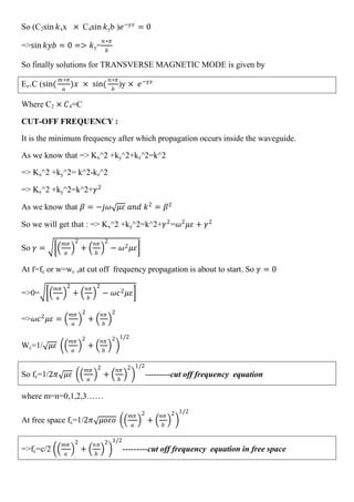
![CUT – OFF WAVELENGTH:
This is given by
ƴ𝑐 =
𝑐
𝑓
= 2 × (
1
𝑚𝜋
𝑎
2
+
𝑛𝜋
𝑏
2 1/2)
DOMINANT MODE :
The mode having lowest cut-off frequency or highest cut-off wavelength is called
DOMINANT MODE.
*the mode can be TM01,TM10,TM11,But for TM10 and TM01,wave can’t exist.
*hence TM11has lowest cut-off frequency and is the DOMINANT MODE in case of all TM
modes only.
PHASE CONSTANT :
As we know that 𝛾 =
𝑚𝜋
𝑎
2
+
𝑛𝜋
𝑏
2
− 𝜔2
𝜇𝜀
1/2
So j𝛽 = 𝜔2 𝜇𝜀 − 𝜔𝑐2 𝜇𝜀
This condition satisfies that only 𝜔𝑐2
𝜇𝜀 > 𝜔2
𝜇𝜀
So that 𝛽 = 𝜔2 𝜇𝜀 − 𝜔𝑐2 𝜇𝜀
PHASE VELOCITY :
It is given by Vp=𝜔/ 𝛽
Vp=
𝜔
(𝜔2 𝜇𝜀 −𝜔𝑐 2 𝜇𝜀 )
Vp=1/ [ 𝜔𝜀(1 − 𝑓𝑐2
/𝑓2
)]
GUIDE WAVELENGTH :
It is given by 𝜆𝑔 =
2𝜋
𝛽
=
2𝜋
𝜔2 𝜇𝜀 −𝜔𝑐 2 𝜇𝜀
𝜆𝑔 =1/ (𝑓2
𝜇𝜀 − 𝑓𝑐2
𝜇𝜀)
𝜆𝑔 =
𝑐
𝑓
/(1 − 𝑓𝑐2
/𝑓2
)
𝜆𝑔 =
𝜆𝑜
[1−
𝜆𝑜
𝜆𝑐
2
]
1
2](https://image.slidesharecdn.com/microwaveengineering-160418161558/85/Microwave-Engineering-Lecture-Notes-17-320.jpg)
![
1
𝜆𝑔2
=1/ 𝜆𝑜2
−
1
𝜆𝑐2
CASE -2
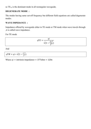
SOLUTIONS OF TRANSVERSE ELECTRIC MODE :
Here Ez=0 and Hz≠ 0
Hz=(B1cos 𝑘𝑥𝑥 +B2sin 𝑘xx)( B3cos 𝑘𝑦𝑦 +B4sin 𝑘yy ) 𝑒−𝛾𝑧
B1,B2,B3,B4,KX,KY are found from boundary conditions.
𝐸𝑥 = 0 𝑓𝑜𝑟 𝑦 = 0 𝑎𝑛𝑑 𝑦 = 𝑏
𝐸𝑦 = 0 𝑓𝑜𝑟 𝑥 = 0 𝑎𝑛𝑑 𝑥 = 𝑎
At x=0 and y=0 ;
Ey =
J𝜔𝜇
h2
𝜕
𝜕𝑥
𝐻𝑧 −
Ƴ
2
𝜕
𝜕𝑦
𝐸𝑧 ,as
Ƴ
2
𝜕
𝜕𝑦
𝐸𝑧 = 0
So Ey =
J𝜔𝜇
h2
𝜕
𝜕𝑥
𝐻𝑧
Here
𝜕
𝜕𝑥
𝐻𝑧 = [B1 ∗ kx ∗ (−sin 𝑘𝑥𝑥) + B2 ∗ kx ∗ cos 𝑘 xx)( B3 cos 𝑘𝑦𝑦 + B4 sin 𝑘 yy ) 𝑒−𝛾𝑧
]
So Ey =
J𝜔𝜇
h2
[B1 ∗ kx ∗ (−sin 𝑘𝑥𝑥) + B2 ∗ kx ∗ cos 𝑘 xx)( B3 cos 𝑘𝑦𝑦 + B4 sin 𝑘 yy ) 𝑒−𝛾𝑧
]
At x=0,
𝜕
𝜕𝑥
𝐻𝑧 = 0
0=[B2*Kx][(B3cosKyy+B4sinKyy)𝑒−𝛾𝑧
]
From this B2=0
So , Ex = −
j𝜔𝜇
h2
𝜕
𝜕𝑦
𝐻𝑧 −
Ƴ
2
𝜕
𝜕𝑥
𝐸𝑧 [as
Ƴ
2
𝜕
𝜕𝑥
𝐸𝑧 = 0];
Ex = −
j𝜔𝜇
h2
𝜕
𝜕𝑦
𝐻𝑧
Here
𝜕
𝜕𝑦
𝐻𝑧 = [B1 (cos 𝑘𝑥𝑥) + B2 sin 𝑘 xx)(− B3 ∗ ky ∗ sin 𝑘𝑦𝑦 + B4 ∗ ky ∗ cos 𝑘 yy ) 𝑒−𝛾𝑧
]
Ex = −
J𝜔𝜇
h2
[B1 (cos 𝑘𝑥𝑥) + B2 sin 𝑘 xx)(− B3 ∗ ky ∗ sin 𝑘𝑦𝑦 + B4 ∗ ky ∗ cos 𝑘 yy ) 𝑒−𝛾𝑧
]
B1 (cos 𝑘𝑥𝑥) + B2 sin 𝑘 xx)(− B3 ∗ ky ∗ sin 𝑘𝑦𝑦 + B4 ∗ ky ∗ cos 𝑘 yy ) 𝑒−𝛾𝑧
= 0](https://image.slidesharecdn.com/microwaveengineering-160418161558/85/Microwave-Engineering-Lecture-Notes-18-320.jpg)
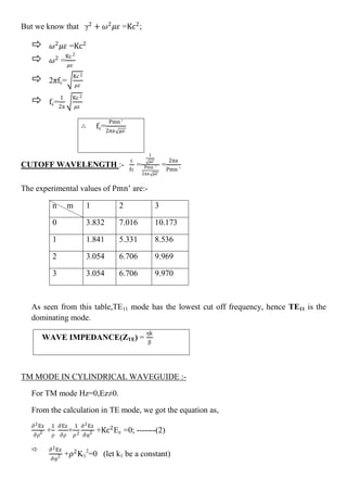
![At y=0 ,
𝜕
𝜕𝑦
𝐻𝑧 = 0
B1 (cos 𝑘𝑥𝑥) + B2 sin 𝑘 xx B4 ∗ ky 𝑒−𝛾𝑧
= 0
From this B4=0
So Hz= B1 (cos 𝑘𝑥𝑥) ∗ B3 cos 𝑘𝑦𝑦 * 𝑒−𝛾𝑧
𝜕
𝜕𝑥
𝐻𝑧 = [B1 ∗ kx ∗ (−sin 𝑘𝑥𝑥) ( B3 cos 𝑘𝑦𝑦 ) 𝑒−𝛾𝑧
]
Here we know that at x=a,Ey=0
So Ey=
J𝜔𝜇
h2
[−B1 ∗ kx ∗ (−sin 𝑘𝑥𝑎) ∗ B3 cos 𝑘𝑦𝑦 ∗ 𝑒−𝛾𝑧
]=0
sin 𝑘𝑥𝑎 = 0 => 𝑘𝑥 =
𝑚𝜋
𝑎
At y=b,Ex=0
So Ex=−
J𝜔𝜇
h2
[B1 (cos 𝑘𝑥𝑥) (B3 ∗ ky ∗ sin 𝑘𝑦𝑏) 𝑒−𝛾𝑧
]=0
So here
sin 𝑘𝑦𝑏 = 0 => 𝑘𝑦 =
𝑛𝜋
𝑏
So the general TRANSVERSE ELECTRIC MODE solution is given by
Hz=B (cos
𝑚𝜋
𝑎
𝑥) (cos
𝑛𝜋
𝑏
𝑦) 𝑒−𝛾𝑧
Where B=B1B3
CUT-OFF FREQUENCY :
The cut-off frequency is given as
fc=c/2
𝑚𝜋
𝑎
2
+
𝑛𝜋
𝑏
2 1/2
---------cut off frequency equation in free space
DOMINANT MODE :
The mode having lowest cut-off frequency or highest cut-off wavelength is called
DOMINANT MODE.here TE00 where wave can’t exist.
So fc(TE01)=c/2b
fc(TE10)=c/2a
for rectangular waveguide we know that a>b](https://image.slidesharecdn.com/microwaveengineering-160418161558/85/Microwave-Engineering-Lecture-Notes-19-320.jpg)
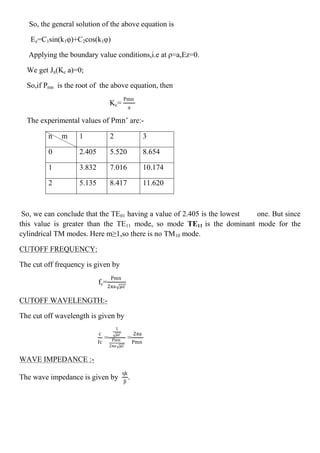
![CYLINDRICAL WAVEGUIDES
A circular waveguide is a tubular, circular conductor. A plane wave propagating through a
circular waveguide results in transverse electric (TE) or transverse magnetic field(TM)
mode.
Assume the medium is lossless(α=0) and the walls of the waveguide is perfect
conductor(σ=∞).
The field equations from MAXWELL’S EQUATIONS are:-
∇xE=-jωμH ------(1.a)
∇xH=jωϵE -----(1.b)
Taking the first equation,
∇xE=-jωμH
Expanding both sides of the above equation in terms of cylindrical coordinates, we get
1
𝜌
*|
𝐴𝜌 𝜌𝐴𝜑 𝐴𝑧
𝜕/𝜕𝜌 𝜕/𝜕𝜑 𝜕/𝜕𝑧
𝐸𝜌 𝜌𝐸𝜑 𝐸𝑧
| =-j𝜔𝜇[𝐻𝜌𝐴𝜌 + 𝐻𝜑𝐴𝜑 + 𝐻𝑧𝐴𝑧]
Equating :-
1
𝜌
𝜕 𝐸𝑧
𝜕𝜑
−
𝜕(𝜌𝐸𝜑 )
𝜕𝑧
=-jωμH𝜌 ------ (2.a)
𝜕 𝐸𝜌
𝜕𝑧
−
𝜕(𝐸𝑧)
𝜕𝜌
=-jωμH𝜑 ------ (2.b)
1
𝜌
𝜕 𝜌𝐸𝜑
𝜕𝜌
−
𝜕(𝐸𝜌)
𝜕𝜑
=-jωμH𝑧 ------- (2.c)
Similarly expanding ∇xH=jωϵE,
1
𝜌
*|
𝐴𝜌 𝜌𝐴𝜑 𝐴𝑧
𝜕/𝜕𝜌 𝜕/𝜕𝜑 𝜕/𝜕𝑧
𝐻𝜌 𝜌𝐻𝜑 𝐻𝑧
| =j𝜔𝜖[𝐸𝜌𝐴𝜌 + 𝐸𝜑𝐴𝜑 + 𝐸𝑧𝐴𝑧]
Equating:
1
𝜌
𝜕 𝐻𝑧
𝜕𝜑
−
𝜕(𝜌𝐻𝜑 )
𝜕𝑧
= jωϵE𝜌 ------ (3.a)
𝜕 𝐻𝜌
𝜕𝑧
−
𝜕(𝐻𝑧)
𝜕𝜌
=-jωϵE𝜑 ------- (3.b)
1
𝜌
𝜕 𝜌𝐻𝜑
𝜕𝜌
−
𝜕(𝐻𝜌)
𝜕𝜑
=jωϵE𝑧 ------- (3.c)](https://image.slidesharecdn.com/microwaveengineering-160418161558/85/Microwave-Engineering-Lecture-Notes-21-320.jpg)
![Let us assume that the wave is propagating along z direction. So,
Hz=𝑒−𝛾𝑧
;
=>
𝜕𝐻𝑧
𝜕𝑧
= −𝛾𝑒−𝛾𝑧
𝜕
𝜕𝑧
= −𝛾
Putting in equation 2 and 3:
𝜕 𝐸𝑧
𝜕𝜑
+ 𝛾𝜌𝐸𝜑 =-jωμ𝜌H𝜌 ------ (4.a)
𝛾𝐸𝜌 +
𝜕(𝐸𝑧)
𝜕𝜌
=jωμ𝜌H𝜑 ------- (4.b)
𝜕 𝜌𝐸𝜑
𝜕𝜌
−
𝜕(𝐸𝜌)
𝜕𝜑
=-jωμ𝜌H𝑧 ------- (4.c)
And
1
𝜌
𝜕 𝐻𝑧
𝜕𝜑
+ 𝛾𝜌𝐻𝜑 =jωϵE𝜌 ------ (5.a)
𝛾𝐻𝜌 +
𝜕(𝐻𝑧)
𝜕𝜌
=jωϵE𝜑 ------- (5.b)
1
𝜌
𝜕 𝜌𝐻𝜑
𝜕𝜌
−
𝜕(𝐻𝜌)
𝜕𝜑
=jωϵE𝑧 ------- (5.c)
Now from eq(4.a) and eq(5.b),we get
H𝜌 =
1
−jωμ𝜌
𝜕 𝐸𝑧
𝜕𝜑
+ 𝛾𝜌𝐸𝜑 ; H𝜌=
1
𝛾
[-jωϵE𝜑-
𝜕(𝐻𝑧)
𝜕𝜌
]
∴
1
−jωμ𝜌
𝜕 𝐸𝑧
𝜕𝜑
+ 𝛾𝜌𝐸𝜑 =
1
𝛾
[-jωϵE𝜑-
𝜕(𝐻𝑧)
𝜕𝜌
]
=>
1
𝜌
𝜕 𝐸𝑧
𝜕𝜑
+ 𝛾𝐸𝜑= -
𝜔2 𝜇𝜀
𝛾
E𝜑 +
jωμ
γ
∂Hz
∂ρ
=> (
γ2+𝜔2 𝜇𝜀
γ
)Eφ =
jωμ
γ
∂Hz
∂ρ
-
1
ρ
∂Hz
∂ρ
Let (γ2
+ 𝜔2
𝜇𝜀) =h2
=Kc2
;
For lossless medium α=0;γ=jβ;
Now the final equation for Eφ is](https://image.slidesharecdn.com/microwaveengineering-160418161558/85/Microwave-Engineering-Lecture-Notes-22-320.jpg)
![Eφ =
−j
Kc2
(
β
ρ
∂Ez
∂φ
− ωμ
∂Hz
∂ρ
) ----- (6.a)
Hφ =
−j
Kc2
(ωε
∂Ez
∂ρ
+
β
ρ
∂Hz
∂φ
) ----- (6.b)
Eρ =
−j
Kc2
(
ωμ
ρ
∂Hz
∂φ
+ β
∂Ez
∂ρ
) ----- (6.c)
Hρ=
j
Kc2
(
ωε
ρ
∂Ez
∂φ
− β
∂Hz
∂ρ
) ------ (6.d)
Equations (6.a),(6.b),(6.c),(6.d) are the field equations for cylindrical waveguides.
TE MODE IN CYLINDRICAL WAVEGUIDE :-
For TE mode, Ez=0, Hz≠0.
As the wave travels along z-direction,e−γz
is the solution along z-direction.
As, γ2
+ 𝜔2
𝜇𝜀 =h2
;
-β2
+ω2
μϵ =Kc2
;
-β2
+K2
=Kc2
(as K2
= 𝜔2
𝜇𝜀)
According to maxwell’s equation, the laplacian of Hz :
∇2
Hz=−𝜔2
𝜇𝜀Hz;
∇2
Hz+𝜔2
𝜇𝜀Hz=0;
∇2
Hz+𝐾2
Hz=0
Expanding the above equation, we get:
∂2Hz
∂ρ2 +
1
ρ
∂Hz
∂ρ
+
1
𝜌2
∂2HZ
∂φ2 +
∂2Hz
∂z2
+K2
Hz =0;
Now, HZ= e−γz
;
∂2Hz
∂z2
=(−γ)2
e−γz
;
∂2Hz
∂z2
=−β2
e−γz
;
∂2Hz
∂z2
=−β2
Hz =>
∂2
∂z2
=−β2
;
Putting this value in the above equations, we get:-
∂2Hz
∂ρ2 +
1
ρ
∂Hz
∂ρ
+
1
𝜌2
∂2HZ
∂φ2 −β2
Hz+K2
Hz =0;
∂2Hz
∂ρ2 +
1
ρ
∂Hz
∂ρ
+
1
𝜌2
∂2HZ
∂φ2 +Kc2
Hz =0; [as -β2
+K2
=Kc2
]](https://image.slidesharecdn.com/microwaveengineering-160418161558/85/Microwave-Engineering-Lecture-Notes-23-320.jpg)
![∂2Hz
∂ρ2 +
1
ρ
∂Hz
∂ρ
+Kc2
Hz = -
1
𝜌2
∂2HZ
∂φ2 ;
The partial differential with respect to ρ and φ in the above equation are equal only when
the individuals are constant (Let it be Ko
2
).
-
1
𝜌2
∂2HZ
∂φ2 = Ko
2
∂2HZ
∂φ2 +𝜌2
Ko
2
=0
Solutions to the above differential equation is:-
Hz = B1sin (Koφ)+B2cos(Koφ)-----{solution along φ direction}.
Now,
∂2Hz
∂ρ2 +
1
ρ
∂Hz
∂ρ
+(Kc2
Hz - Ko
2
)= 0
This equation is similar to BESSEL’S EQUATION,so the solution of this equation is
Hz=CnJn(Kc ρ) --------{solution along 𝜌-direction}
Hence,
Hz=Hz(ρ)Hz(φ)e−γz
;
So, the final solution is,
Hz= CnJn(Kc ρ)[ B1sin (Koφ)+B2cos(Koφ)] e−γz
Applying boundary conditions:-
At ρ=a, Eφ=0 =>
∂Hz
∂ρ
=0,
=> Jn (Kc ρ) =0
=> Jn(Kc a) =0
If the roots of above equation are defined as Pmn’,then
Kc=
Pmn ’
a
;
∴
CUT-OFF FREQUENCY :- It is the minimum frequency after which the propagation
occurs inside the cavity.
∴ γ=0;
Hz= CnJn (
Pmn ’
a
ρ) [ B1sin (Koφ)+B2cos(Koφ)] e−γz](https://image.slidesharecdn.com/microwaveengineering-160418161558/85/Microwave-Engineering-Lecture-Notes-24-320.jpg)
![ω0
2
µ € = (mπ/a)2
+ ( nπ/b)2
+ (lπ/d)2
or ω0 =
𝟏
µ€
[(mπ/a)2
+ ( nπ/b)2
+ (lπ/d)2
]1/2
or f0 =
𝟏
𝟐𝝅 µ€
[(mπ/a)2
+ ( nπ/b)2
+ (lπ/d)2
]1/2
or f0=
𝒄′
𝟐
[(mπ/a)2
+ ( nπ/b)2
+ (lπ/d)2
]1/2
This is the expression for resonant frequency of cavity resonator.
The mode having lowest resonant frequency is called DOMINANT MODE and for TE
AND TM the dominant modes are TE-101 and TM-110 respectively.
QUALITY FACTOR OF CAVITY RESONATOR:
Q=2π x
maximum energy stored per cycle
energy dissipated per cycle
FACTORS AFFECTING THE QUALITY FACTOR:
Quality factor depends upon 2 factors:
Lossy conducting walls
Lossy dielectric medium of a waveguide
1) LOSSY CONDUCTING WALL:
The Q-factor of a cavity with lossy conducting walls but lossless dielectric medium
i.e. σc ≠ ∞ and σ =0
Then Qc = (2ω0 We/Pc)
Where w0-resonant frequency
We-stored electrical energy
Pc-power loss in conducting walls
From dimensional point of view:
Qc = (kad3
) (bŋ) x { 1/(2l2
a3
d + l3
a3
d + ad3
+ 2bd3
) } /( 2π2
Rs)
Where k = (ω2
µ€) 1/2
ŋ = ŋi/ 𝝐r = 377/ 𝝐r
2) LOSSY DIELECTRIC MEDIUM:
The Q-factor of a cavity with lossy dielectric medium but lossless conducting walls
i.e. σc=∞ and σ≠0](https://image.slidesharecdn.com/microwaveengineering-160418161558/85/Microwave-Engineering-Lecture-Notes-28-320.jpg)
![=𝑉𝐴 + 𝑉𝑅 + 𝑉𝑖 sin 𝑤𝑡
Neglecting the AC compoment,
𝑉𝐴𝐵 = 𝑉𝑎 + 𝑉𝑅
E =
𝜕𝑉 𝐴𝐵
𝜕𝑥
=
−𝑉 𝐴𝐵
𝑆
=
−(𝑉𝑎+ 𝑉𝑅 )
𝑆
-------(a)
The force experienced on an electron
F=qe=
−𝑞(𝑉𝑎+ 𝑉𝑅)
𝑆
F=
m ∂2x
∂t2
-------(b)
From equations a and b we get
m ∂2x
∂t2
=
−𝑞(𝑉𝑎+ 𝑉𝑅)
𝑆
Integrating both sides we get,
m ∂2x
∂t2
=
−𝑞(𝑉𝑎+ 𝑉𝑅)
𝑆
m ∂x2
=
−𝑞(𝑉𝑎+ 𝑉𝑅)
𝑆
𝑡
𝑡1
𝜕𝑡
m
𝜕𝑥
𝜕𝑡
=
−𝑞(𝑉𝑎+ 𝑉𝑅)
𝑆
𝑡𝑡1
𝑡
𝜕𝑥
𝜕𝑡
=
−𝑞(𝑉𝑎+ 𝑉𝑅)
𝑚𝑆
(t-𝑡1)+ 𝑘1
∴ 𝑘1is called velocity constant and assumed to velocity at (t-𝑡1)
𝜕𝑥
𝜕𝑡
=
−𝑞(𝑉𝑎+ 𝑉𝑅)
𝑚𝑆
(t-𝑡1)+𝑉 𝑡1
𝜕𝑥 =
−𝑞(𝑉𝑎+ 𝑉𝑅)
𝑚𝑆
(t − 𝑡1) ∂ 𝑡 + 𝑉 𝑡1
X=
−𝑞(𝑉𝑎+ 𝑉𝑅 )
𝑚𝑆
[𝑡2
2𝑡1
𝑡
] − 𝑡1 [𝑡]𝑡1
𝑡
+ 𝑉 𝑡1 𝜕𝑡
=
−𝑞(𝑉𝑎+ 𝑉𝑅)
𝑚𝑆
[
𝑡2−𝑡12
2
− 𝑡2 − 𝑡2 𝑡1] + 𝑉 𝑡1 𝜕𝑡
=
−𝑞(𝑉𝑎+ 𝑉𝑅)
𝑚𝑆
𝑡2−𝑡12−2𝑡2 𝑡1+2𝑡2
2
2
+ 𝑉 𝑡1 𝜕𝑡](https://image.slidesharecdn.com/microwaveengineering-160418161558/85/Microwave-Engineering-Lecture-Notes-38-320.jpg)
![The ac component of the current is given by
Iac= 2I0In x′
cos(nωt − φ
∞
𝑛=1
For (n=1),we have fundamental current component ie,
If 2I0I1 x′
cos(nωt − φ
For n=2; cos(nωt − φ) = 1
I2=2IoKiJi(Xi)
Power=
viI2
2
=
vi
2
(2IokiJi Xi )
𝜔 𝑡2 − 𝑡1 = 𝜔
2𝑉 𝑡1 𝑚𝑠
𝑞 𝑉𝑎+ 𝑉𝑅
𝜔𝑡2= 𝜔𝑡1+
2𝑉0 𝑚𝑠𝜔
𝑞 𝑉𝑎+ 𝑉𝑅
[1 +
𝑘 𝑖 𝑣 𝑖
2𝑣 𝑎
sin 𝜔𝑡1]
∴ [
2𝑉0 𝑚𝑠𝜔
𝑞 𝑉𝑎+ 𝑉𝑅
] = 𝛼
𝜔𝑡2= 𝜔𝑡1+𝛼[1 +
𝑘 𝑖 𝑣 𝑖
2𝑣 𝑎
sin 𝜔𝑡1]
𝜔𝑡2= 𝜔𝑡1+𝛼 +
𝑘 𝑖 𝑣 𝑖 𝛼
2𝑣 𝑎
sin 𝜔𝑡1]
Where ,
𝑘 𝑖 𝑣 𝑖 𝛼
2𝑣 𝑎
=x, bunching parameter
Vi=
2va x
αki
=
2va x
(2nπ−
π
2
)ki
Po/p=
2va xI0×Ji x
(2nπ−
π
2
)
Efficiency: η% =
Poutput
Pinput
× 100%
=
2va xI0×Ji x
(2nπ−
π
2
)va xI0
=
2×Ji x
(2nπ−
π
2
)
× 100%
Electronics admittance of reflex klystron
It is defined as the ratio of current induced in the cavity by the modulation of electron beam
to the voltage across the cavity gap.](https://image.slidesharecdn.com/microwaveengineering-160418161558/85/Microwave-Engineering-Lecture-Notes-40-320.jpg)

The document outlines a course curriculum in microwave engineering, covering topics such as high-frequency transmission lines, waveguides, microwave sources, and microwave propagation. It specifies various modules including transmission line theory, design and analysis of waveguides, and the principles of microwave devices and circuits alongside relevant textbooks for reference. Additionally, it highlights types of transmission lines, their characteristics, and the use of the Smith chart for evaluating transmission line parameters.