Downloaded 15 times


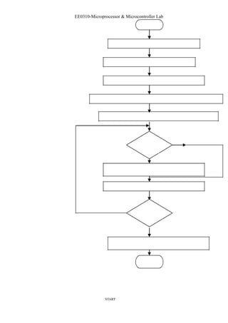


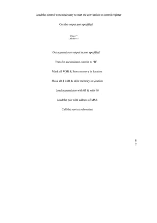
![EE0310-Microprocessor & Microcontroller Lab
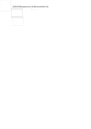
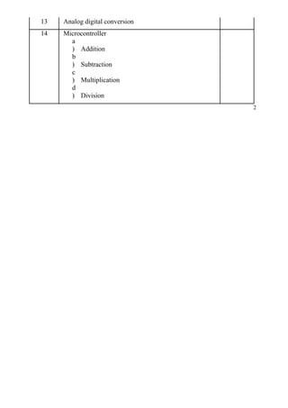
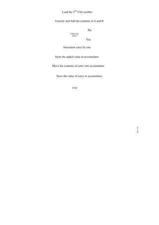
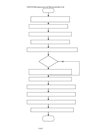
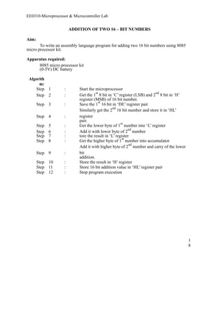
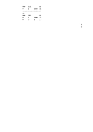
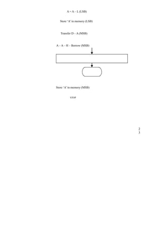
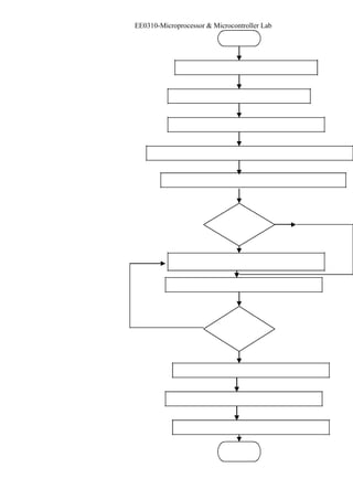
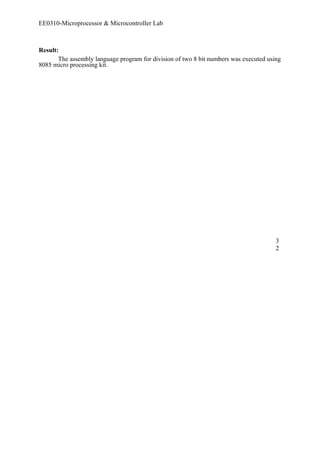
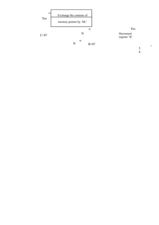
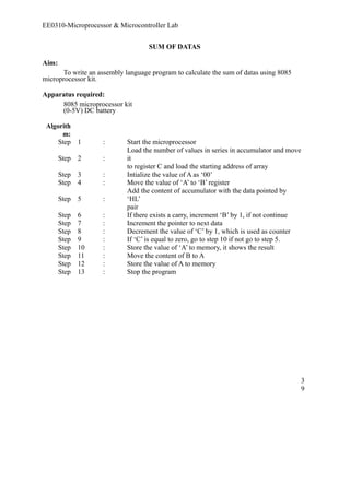
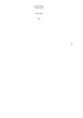
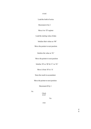
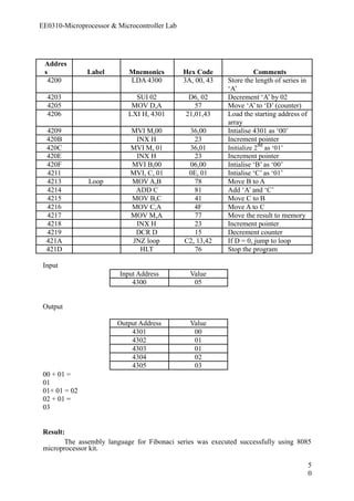
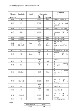
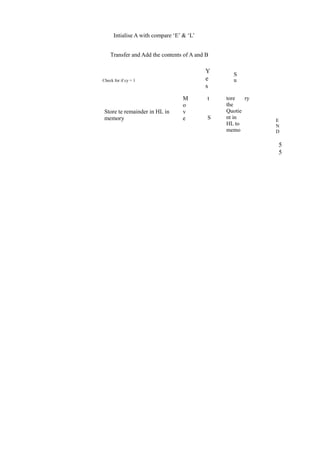
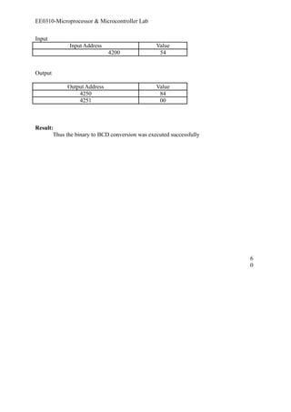
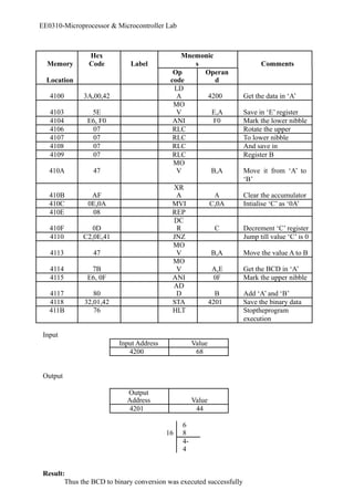
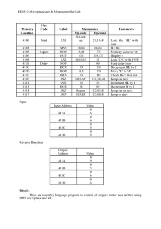
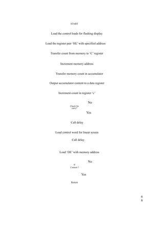
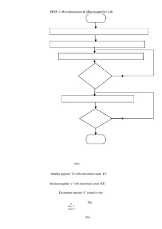
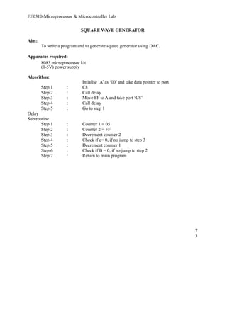
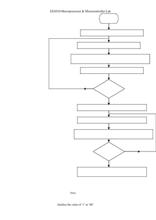
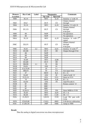
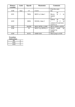
4609 EB XCHG [DE] – [HL]
460A 0D DCR C
Decreme
nt counter
value
460B C4 CNZ Facto
Call on no zero to
facto
460C 00
(i.e
repeat
process
till
460D 46 zero flag for c = 1)
460E C9 RET Return
t
o main
program
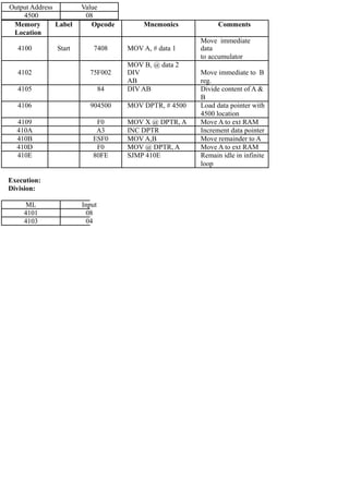
Memory
address Content
4250 04
4251 18
1 x 2 x 3 x 4 = 24
Hexadecimal
16 24
1-8
Result:
Thus, factorial program was done successfully
47](https://image.slidesharecdn.com/microprocessorlabmanual-ee0310-141212025005-conversion-gate02/85/Microprocessorlabmanual-ee0310-74-320.jpg)

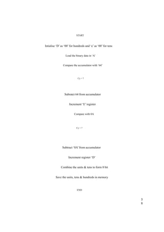


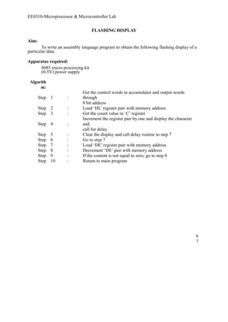

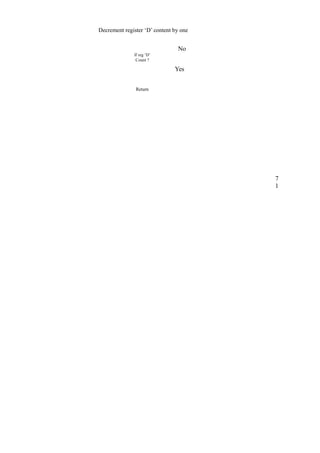
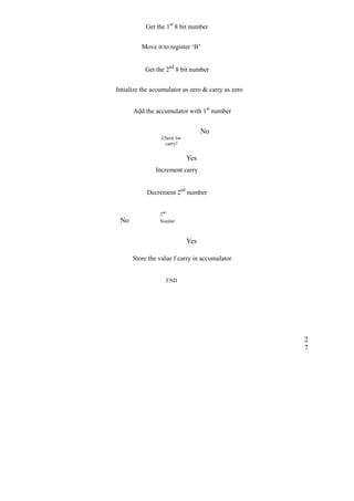
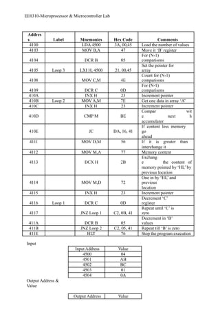
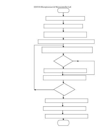
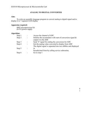
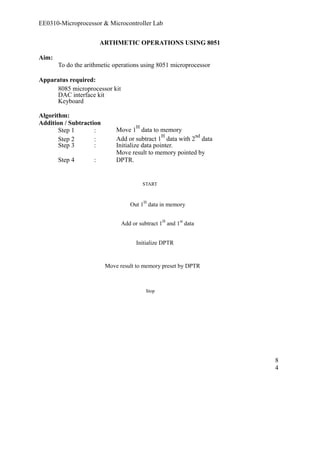
![EE0310-Microprocessor & Microcontroller Lab
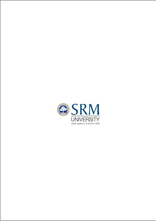
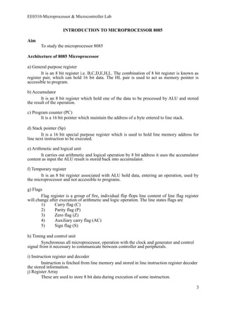
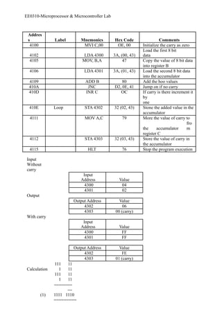
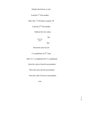
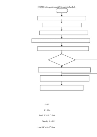
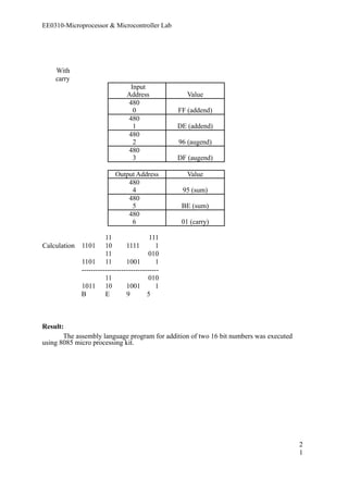
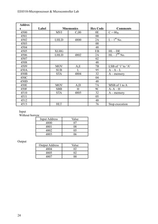
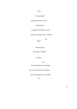
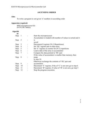
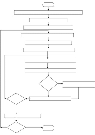
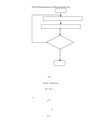
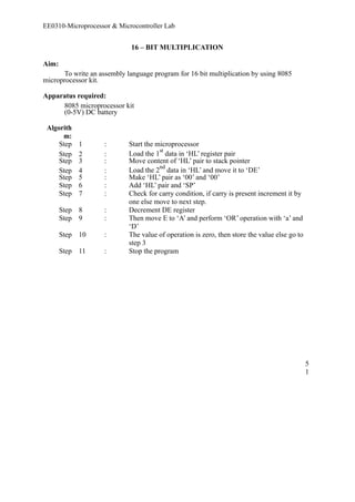
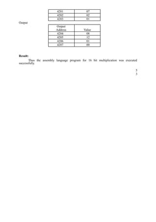
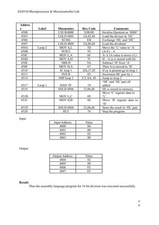
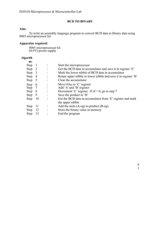
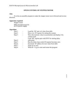
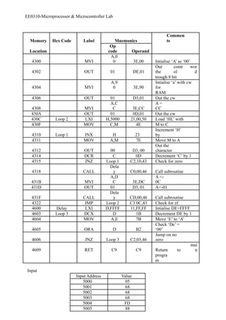
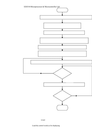
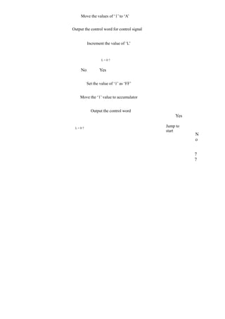
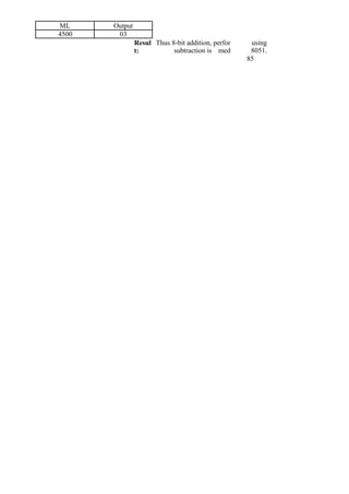
Memory Hex Code Label Mnemonics
Commen
ts
Location Op code Operand
4100 3E,00 Start MVI A,00 Intialise ‘A’ with ‘00’
Load the control
4102 D3,C8 OUT C8
words
4104 CD,11,41 CALL Delay Call delay sutroutine
4107 3E,FF MVI A,FF Intialise ‘A’ with ‘FF
4109 D3,C8 OUT C8 A -> C8
410B CD,11,41 CALL Delay Call delay subroutine
410E C3,00,41 JMP Start Jump to start
4111 06,05 Delay MVI B,05 B -> 05
[C] =>
4113 0E Loop 1 MVI C,FF
FF
4115 OD Loop 2 DCR C Decrement ‘C’ register
Jump on no
4116 C2,15,41 JNZ Loop 2
zero
4119 05 DCR B Decrement ‘B’ register
411A C2,13,41 JNZ Loop 1 Jump on n zero
mai
411D C9 RET Return to
n
program
Result:
Thus square wave was generated using 8085 microprocessor kit.
75](https://image.slidesharecdn.com/microprocessorlabmanual-ee0310-141212025005-conversion-gate02/85/Microprocessorlabmanual-ee0310-122-320.jpg)
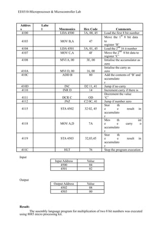
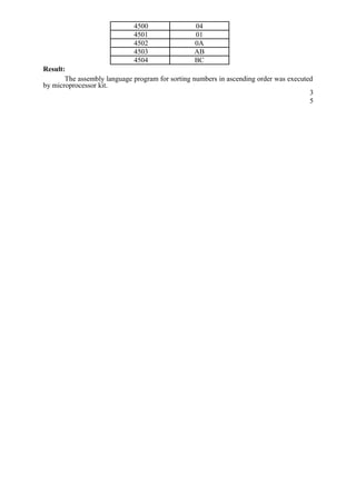
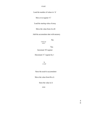
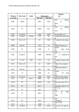
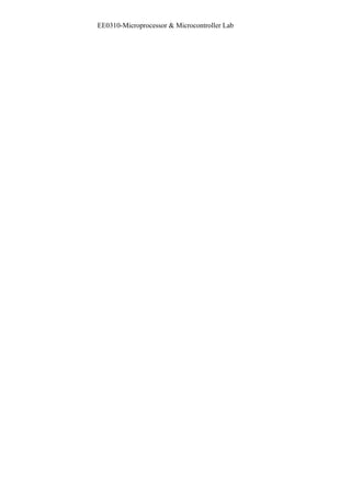
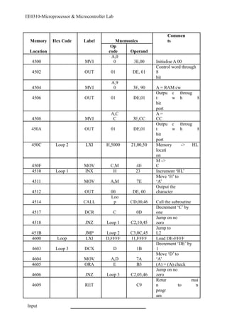
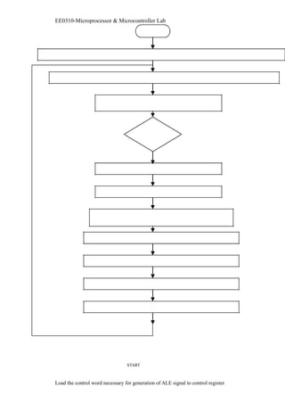
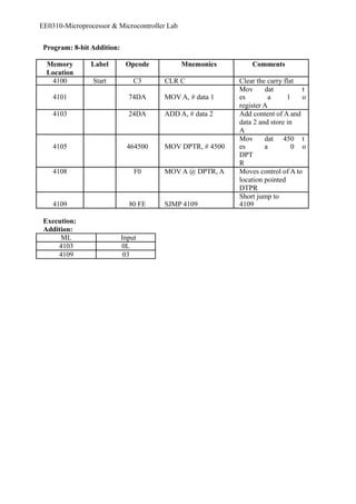
![EE0310-Microprocessor & Microcontroller Lab
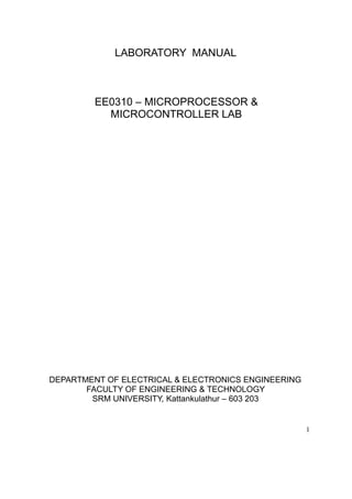
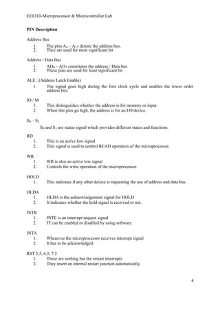
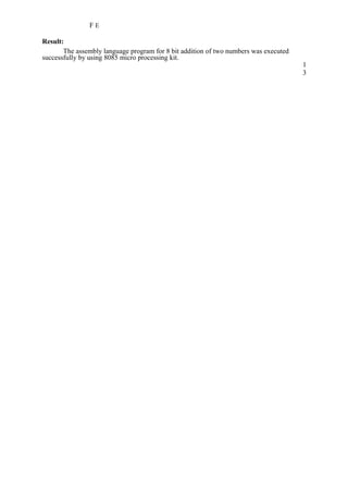
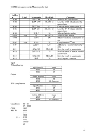
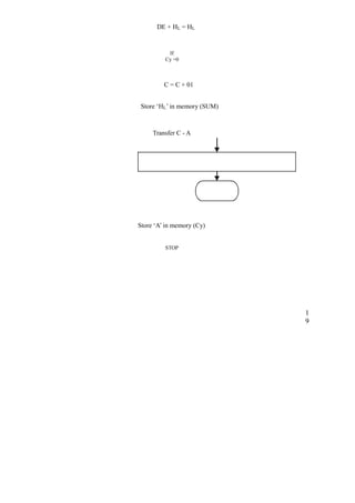
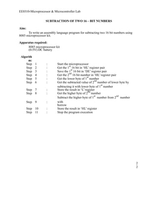
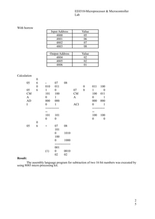
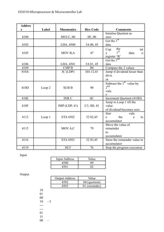
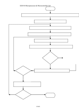
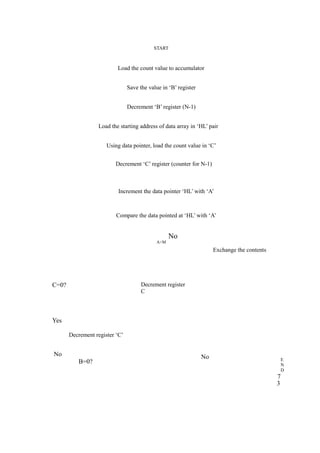
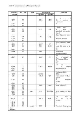
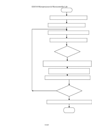
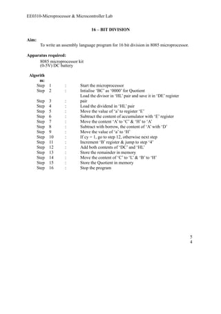
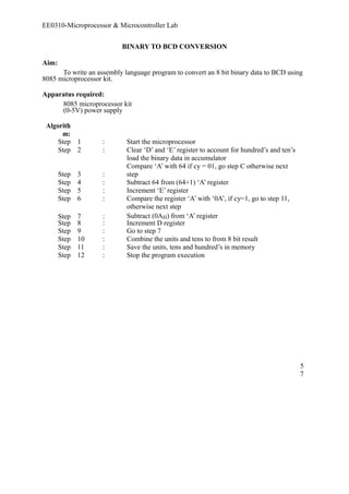
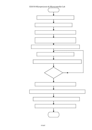
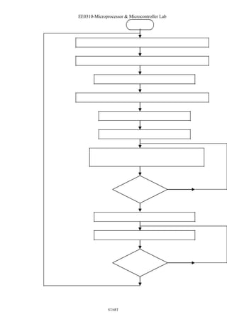
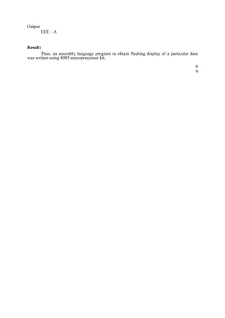
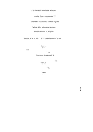
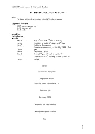
Memory Hex Code Label Mnemonics Comments
Location Op code Operand
4300 2E,00 Start MVI L,00 Intialise ‘L’ as ‘00’
4302 7D Loop 1 MOV A,L [L] -> [A]
Load the control
4303 D3,C8 OUT C8
words
4305 2C INR L Increment register ‘L’
4306 C2,02,43 JNZ Loop 1 Jump on no zero to
loop 1
4309 2E, FF MVI L,FF L = FF
430B 70 Loop 2 MOV A,L L -> A
430C D3,C8 OUT C8 [C8] -> [A]
430E 2D DCR L Decrement L by one
430F C2,0B,43 JNZ Loop 2 Jump on no zero to
430B
4312 C3,00.43 JMP Start Repeat process
Result:
Thus the triangular wave was generated using 8085 microprocessor kit.
78](https://image.slidesharecdn.com/microprocessorlabmanual-ee0310-141212025005-conversion-gate02/85/Microprocessorlabmanual-ee0310-126-320.jpg)
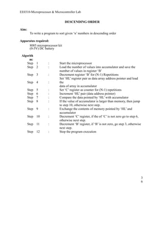
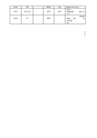
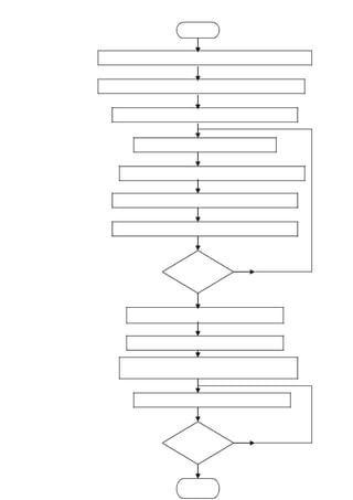
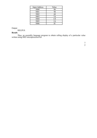
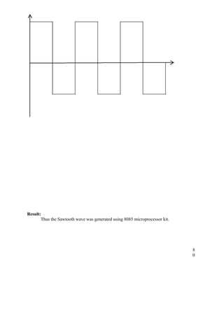
![EE0310-Microprocessor & Microcontroller Lab
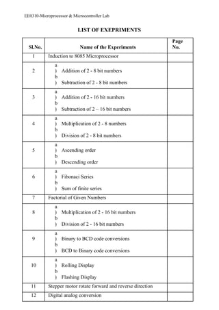
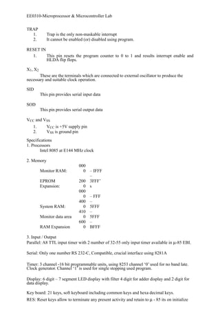
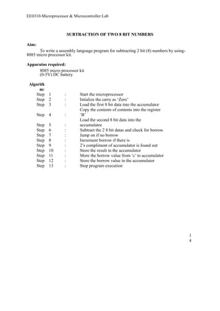
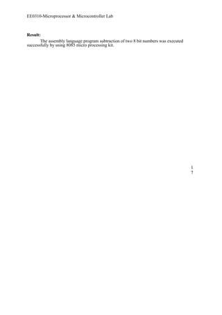
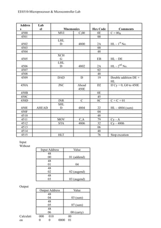
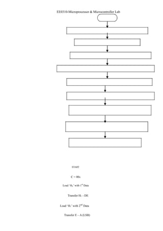
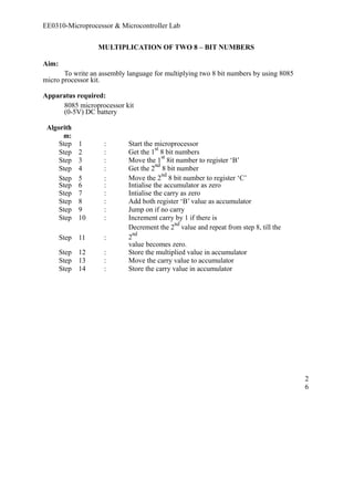
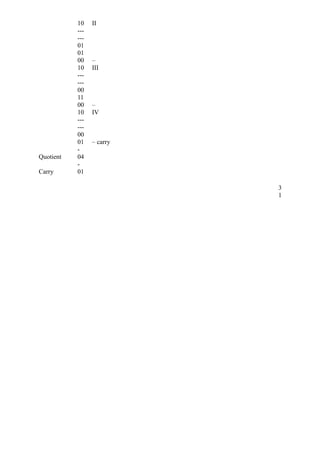
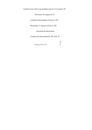
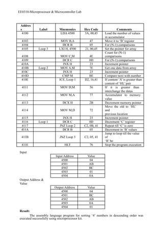
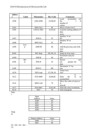
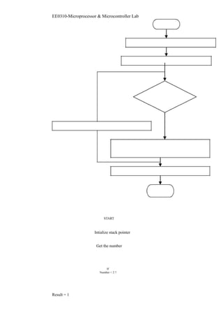
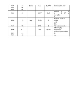
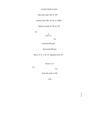
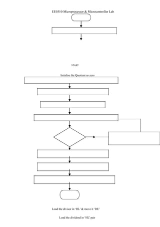
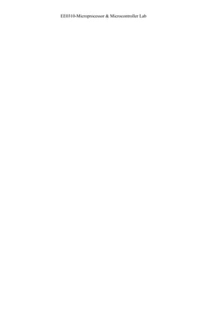
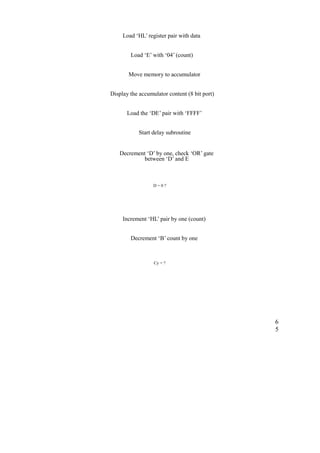
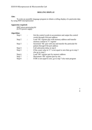
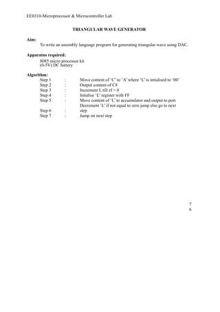
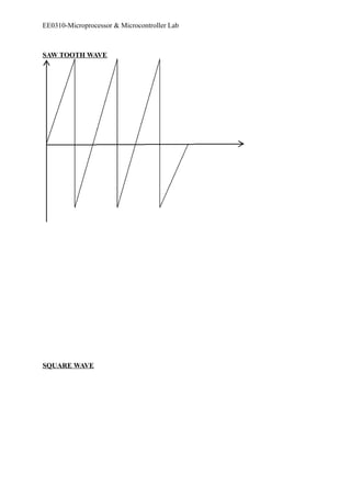
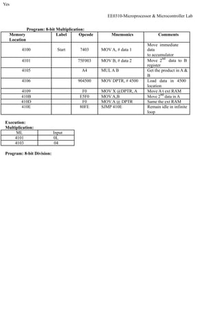
SAWTOOTH WAVE GENERATOR
Aim:
To write an assembly language program for generating Sawtooth waveform by using
microprocessor 8085.
Apparatus required:
8085 microprocessor kit
(0-5V) power supply
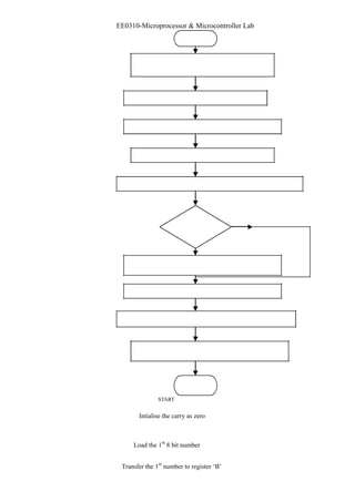
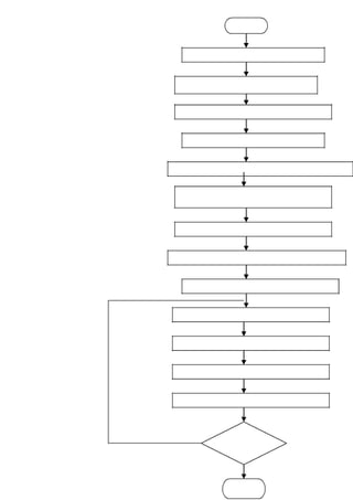
Algorithm:
Step
1 : Intialise accumulator with ‘00’
Step
2 : Output current address specified
Step
3 : Increment accumulator by one
Step
4 : Jump to step one
Del
ay
Intialise the accumulator as
‘00’
Display the output port using
cw
Increment the accumulator
Jump to loop 1
Memory
Hex
Code Label Mnemonics Comments
Location Op code
Operan
d
4500 3E,00 Start MVI A,00 Intialise ‘A’ as ‘00’
Loop
4502 D3, C8
1 OUT
C8
A = [C8]
4504 3C INR A Increment ‘A’ by one
4505 C3,02,45 JMP Loop 1 Jump to loop one
TRIANGULAR WAVE](https://image.slidesharecdn.com/microprocessorlabmanual-ee0310-141212025005-conversion-gate02/85/Microprocessorlabmanual-ee0310-127-320.jpg)

This document contains information about experiments to be performed in the EE0310 Microprocessor and Microcontroller lab. It lists 14 experiments involving operations like addition, subtraction, multiplication, and division using the 8085 microprocessor. It also describes experiments with microcontrollers, stepper motors, and digital to analog conversion. The document provides details of the 8085 architecture, pin descriptions, specifications of the trainer kit used, and sample algorithms for experiments like addition of two 8-bit numbers.


![[Deck] What's New in Spark-Iceberg Integration via DSV2.pptx](https://cdn.slidesharecdn.com/ss_thumbnails/deckwhatsnewinspark-icebergintegrationviadsv2-260210005337-25955b12-thumbnail.jpg?width=640&height=640&fit=bounds)


