Downloaded 63 times
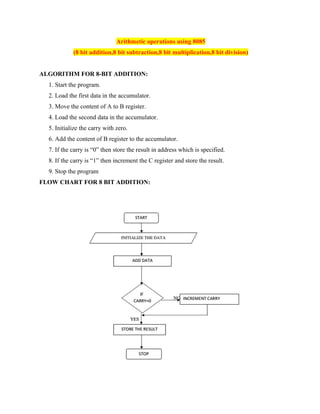

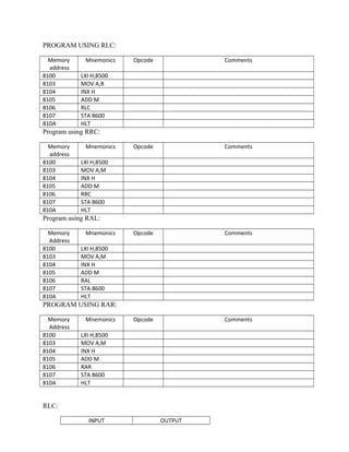
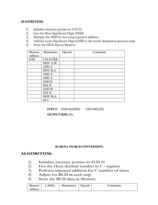
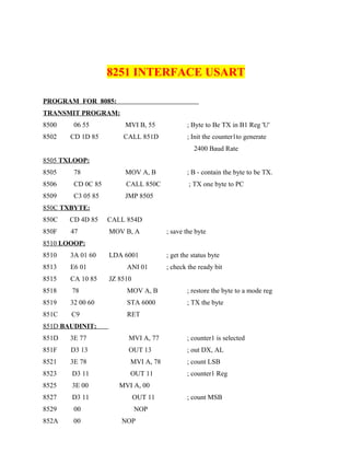
![8100 LXI H,8200
MOV D,00
XRA A
MOV C,M
LOOP 2: ADI 01
DAA
JNC LOOP1
INR D
LOOP1: DCR C
JNZ LOOP2
STA 8300
MOV A,D
STA 8301
HLT
INPUT: 8200-FF
OUTPUT: 8300-55(LSB) 8301-02(MSB)
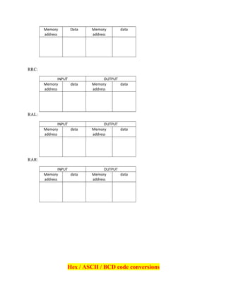
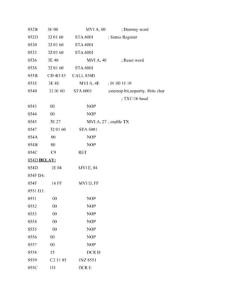
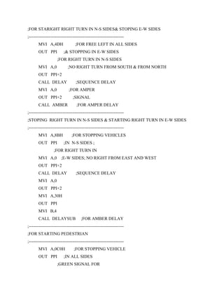
8 CHANNEL ADC INTERFACE with 8085
PROCEDURE:
1. Connect the 26pin FRC to kit and insert power cable.
2. Switch ON the trainer kit.
3. Check all 8 channel input’s and measure it.
4. Enter the given ADC program into the MP/MC kit.
5. If the channel selection is pb2 to pb0 [0 0 0] the CH0 will connect to the MUX output
line. Now we get to CH0 corresponding digital value see in LCD. Similarly CH0 to](https://image.slidesharecdn.com/8085alpprograms-141204102943-conversion-gate01/85/8085-alp-programs-19-320.jpg)
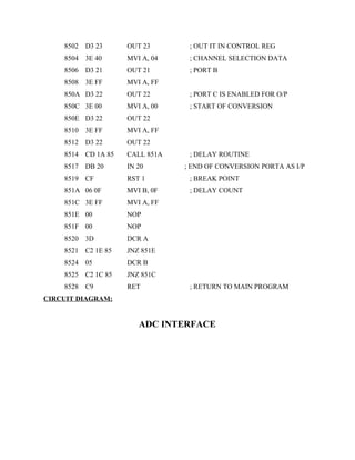
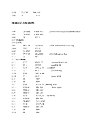
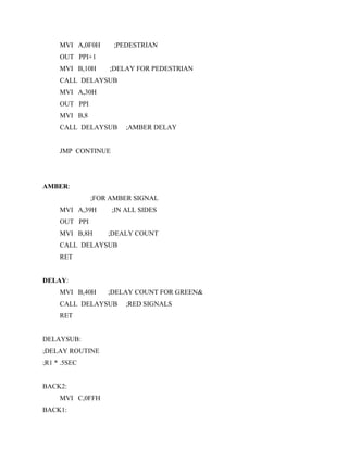
![CH7are connected to the MUX output line based on the status of the channel selection
for pb2to pb0.
6. Execute the program.
7. Now check stepno.3
8. Repeat the steps 3 and 5. Observe the multiplexer output and ADC output
TRUTH TABLE CHANNEL SELECTION:
INPUT CHANNEL
SELECTION
HEX
VALUEPB2 PB1 PB0
0 0 0 CHANNEL 0 00
0 0 1 CHANNEL 1 01
0 1 0 CHANNEL 2 02
0 1 1 CHANNEL 3 03
1 0 0 CHANNEL 4 04
1 0 1 CHANNEL 5 05
1 1 0 CHANNEL 6 06
1 1 1 CHANNEL 7 07
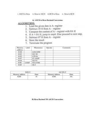
ADC CALCULATION:
Calculate 1count value.
V.REF*2/digital count = 1count
2.5v*2/256 = .0195313v = 19mv
Calculate voltage vs digital count.
[E:g]
2500mv/19mv = 131.57895
Decimal value Hexadecimal value
131.57895 83
PROGRAM:
8500 3E 90 MVI A, 90 ; CONTROL WORD FOR PORT A AS I/P
; PORT B AND PORT C AS O/P](https://image.slidesharecdn.com/8085alpprograms-141204102943-conversion-gate01/85/8085-alp-programs-20-320.jpg)
This document discusses arithmetic operations and conversions using the 8085 microprocessor. It includes algorithms and programs for 8-bit addition, subtraction, multiplication, and division. It also covers sorting algorithms to find the ascending and descending order of numbers, and algorithms to find the minimum and maximum numbers in a data set. Additionally, it explains programs that demonstrate the rotate instructions RLC, RRC, RAL, and RAR. Finally, it provides examples of conversions between ASCII, hexadecimal, and BCD codes.