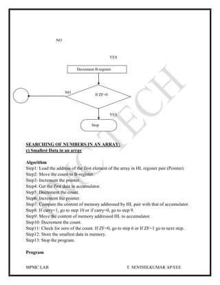
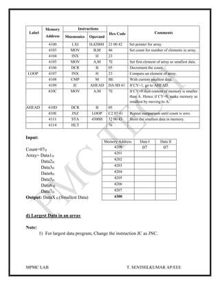
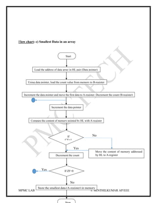
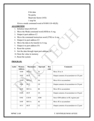
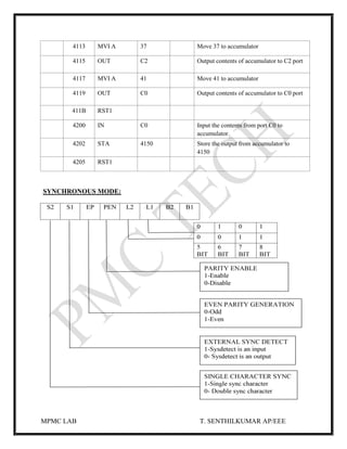
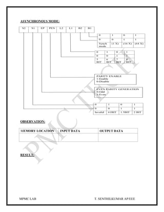
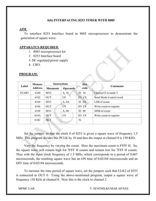
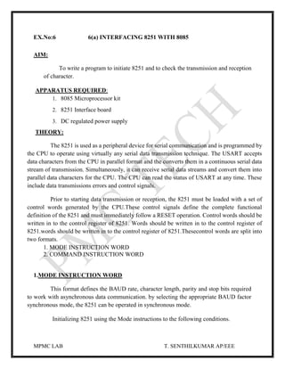
MPMC LAB T. SENTHILKUMAR AP/EEE
ER. PERUMAL MANIMEKALAI COLLEGE OF ENGINEERING
Accredited By NAAC with B++ Grade
DEPARTMENT OF ELECTRICAL AND ELECTRONICS ENGG
LAB MANUAL
VI SEM
EE 8681- MICRO PROCESSOR AND MICRO CONTROLLER LABORATORY
Prepared By
T.SENTHILKUMAR
MPMC LAB T. SENTHILKUMAR AP/EEE
SYLLABUS
EE 8681-MICROPROCESSOR AND MICRO CONTROLLER LABORATORY
AIM
1. To understand programming using instruction sets of processors.
2. To study various digital & linear.
8-bit Microprocessor
1. Simple arithmetic operations:
Multi precision addition / subtraction / multiplication / division.
2. Programming with control instructions:
Increment / Decrement, Ascending / Descending order, Maximum / Minimum of
numbers, Rotate instructions - Hex / ASCII / BCD code conversions.
3. Interface Experiments:
• A/D Interfacing.
• D/A Interfacing.
• Traffic light controller.
4. Interface Experiments: Simple experiments using 8251, 8279, 8254.
8-bit Microcontroller
5. Demonstration of basic instructions with 8051 Micro controller execution,
including:
• Conditional jumps, looping
• Calling subroutines.
• Stack parameter testing
6. Parallel port programming with 8051 using port 1
facility: Stepper motor and D / A converter.
7. Study of Basic Digital IC’s
(Verification of truth table for AND, OR, EXOR, NOT, NOR, NAND, JK FF, RS FF,
D FF)
8. Implementation of Boolean Functions, Adder / Subtractor circuits.
9. Combination Logic; Adder, Subtractor, Code converters, Encoder and Decoder.
10. Sequential Logic; Study of Flip-Flop, Counters (synchronous and asynchronous), Shift
Registers.
MPMC LAB T. SENTHILKUMAR AP/EEE
LIST OF EXPERIMENTS
Ex.No Name of the Experiments Page No.
8 – BIT MICROPROCESSOR (8085)
1 SIMPLE ARITHMETIC OPERATIONS USING 8085
a) 8- bit Addition
b) 8 – bit Subtraction
c) 8- bit Multiplication
d) 8- bit Division
2 SORTING AND SEARCHING OF AN ARRAY USING 8085
a) Ascending order
b) Descending order
c) Largest of a given numbers
d) Smallest of a given numbers
3 CODE CONVERSIONS USING 8085
a) Code Conversion: ASCII to Hexadecimal
b) Code Conversion: Hexadecimal to ASCII
c) Code Conversion: BCD to Hexadecimal
d) Code Conversion: Hexadecimal to BCD
4 INTERFACING A/D AND D/A CONVERTER WITH 8085
a) Interfacing: ADC with 8085
b)Interfacing: DAC with 8085
5 Interfacing: Traffic Light Controller with 8085
6 6(a)Interfacing: 8251 with 8085
MPMC LAB T. SENTHILKUMAR AP/EEE
6(b) Interfacing: 8279 with 8085
6(c) Interfacing: 8253/8254 with 8085
MICROCONTROLLER (8051)
7
7(a) Sum of elements in an array
7(b) Sum using Stack
7( c) Sum using call option
8
8(a) Interfacing: Stepper Motor with 8051
8(b) Interfacing: DAC with 8051
MPMC LAB T. SENTHILKUMAR AP/EEE
EX.No:1 SIMPLE ARITHMETIC OPERATIONS USING 8085
AIM:
To write 8085 assembly language programs to perform arithmetic operations like
Addition, Subtraction, Multiplication and Division over 8-bit data and to test the programs.
APPARATUS REQUIRED:
S.No Description Quantity
1 8085Microprocessor Trainer kit 1
2 DC Power supply 1
a) 8-bit addition
Algorithm:
Step1: Initialize carry with zero.
Step2: Get the Augend.
Step3: Get the Addend.
Step4: Perform addition operation between Augend and Addend.
Step5: Check whether carry =1 If Yes increment Carry, otherwise go to SAVE.
Step6: Store the Sum and Carry.
Program:
Label
Memory
Address
Instructions
Hex Code Comments
Mnemonics Operand
4100 MVI C, 00H 0E 00 Initialize C register (carry) with zero.
4102 LDA 4200H 3A 00 42 Load the first data (Augend) from memory
into the accumulator.
4105 MOV B, A 47 Move Accumulator content to B register.
4106 LDA 4201H 3A 01 42 Load the second data (Addend) from
memory into the accumulator.
4109 ADD B 80 Add accumulator content with B register.
410A JNC SAVE D2 0E 41 If there is no carry, go to SAVE.
410D INR C 0C Increment the C register (carry).
SAVE 410E STA 4202H 32 02 42 Store the accumulator (sum) content in the
location 4202H.
4111 MOV A, C 79 Move C register (carry) content to
accumulator.
MPMC LAB T. SENTHILKUMAR AP/EEE
4112 STA 4203H 32 03 42 Store the accumulator (carry) content in the
location 4203H.
4115 HLT 76 Stop the program
Output:
Memory
Location
Data Samples
CommentsI. II. III. IV.
I/P 4200H Augend
4201H Addend
O/P 4202H Sum
4203H Carry
b) 8-bit subtraction
Algorithm:
Step1: Initialize borrow with zero.
Step2: Get the Subtrahend.
Step3: Get the Minuend.
Step4: Perform subtraction operation between Subtrahend and Minuend.
Step5: Check whether borrow =1, If Yes increment borrow and complement
Differences then add 01H, otherwise go to SAVE.
Step6: Store the Difference and borrow.
Program:
Label
Memory
Address
Instructions
Hex Code Comments
Mnemonics Operand
4100 MVI C, 00H 0E 00 Initialize C register (borrow) with zero.
4102 LDA 4201H 3A 01 42 Load the first data (subtrahend) from
memory into the accumulator.
4105 MOV B, A 47 Move Accumulator content to B register.
4106 LDA 4200H 3A 00 42 Load the second data (minuend) from
memory into the accumulator.
4109 SUB B 90 Subtract B register from accumulator.
410A JNC SAVE D2 11 41 If there is no borrow, go to SAVE.
410D INR C 0C Increment the C register (borrow).
410E CMA 2F Complement the accumulator.
410F ADI 01H C6 01 Add 01 to the accumulator to get 2’s
complement.
SAVE 4111 STA 4202H 32 02 42 Store the accumulator (difference) content
in the location 4202H.
MPMC LAB T. SENTHILKUMAR AP/EEE
4114 MOV A, C 79 Move C register (borrow) content to
accumulator.
4115 STA 4203H 32 03 42 Store the accumulator (borrow) content in
the location 4203H.
4118 HLT 76 Stop the program.
Output:
Memory
Location
Data Samples
CommentsI. II. III. IV.
I/P 4200H Minuend
4201H Subtrahend
O/P 4202H Difference
4203H Borrow
c) 8-bit multiplication
Algorithm:
Step1: Initialize memory pointer and product with zero.
Step2: Get the multiplier and Multiplicand.
Step3: Add product with multiplicand.
Step4: Check whether carry =1, If Yes increment MSB of product by one.
Step5: Decrement multiplier by one.
Step6: Check whether multiplier is zero, if NO go to step3 and repeat this until
multiplier Becomes zero.
Step7: Save product (LSB & MSB).
Program:
Label
Memory
Address
Instructions
Hex Code CommentsMnemoni
cs
Operand
4100 MVI C, 00H 0E 00 Initialize C register (carry) with zero.
4102 LXI H,4200H 21 00 42 Load H-L pair with the address 4200H.
4105 XRA A AF Clear Accumulator.
4106 MOV B, M 46 Get the first data (multiplier) in B register.
4107 INX H 23 Increment to the memory location to get the
next value.
4108 MOV D, M 56 Get the second data (multiplicand) in D
register.
LOOP 2 4109 ADD D 82 Add accumulator content with D register.
410A JNC LOOP 1 D2 0E 41 If CY=0, go to LOOP 1.
410D INR C 0C If CY=1, Increment the C register.
LOOP 1 410E DCR B 05 Decrement the B Register.
410F JNZ LOOP 2 C2 09 41 Repeat addition until ZF=1.
MPMC LAB T. SENTHILKUMAR AP/EEE
4112 INX H 23 Increment to the memory location to get the
next value.
4113 MOV M, A 77 Store LSB of product in memory.
4114 INX H 23 Increment to the memory location to get the
next value.
4115 MOV M,C 71 Store MSB of product in memory.
4116 HLT 76 Stop the program.
Output:
Memory
Location
Data Samples
CommentsI. II. III. IV.
I/P 4200H Multiplier
4201H Multiplicand
O/P 4202H LSB of Product
4203H MSB of Product
d) 8-bit division
Algorithm:
Step1: Initialize Quotient with zero.
Step2: Get the divisor and dividend.
Step3: Compare divisor and dividend.
If divisor < dividend then go to SAVE.
If dividend < divisor then go to next step.
Step5: Subtract divisor from dividend.
Step6: Increment quotient by one and go to step3.
Step7: Store quotient and remainder.
Program:
Label
Memory
Address
Instructions
Hex Code Comments
Mnemonics Operand
4100 MVI C, 00H 0E 00 Clear C register (quotient) with zero.
4102 LDA 4201H 3A 01 42 Load the first data (divisor) in accumulator.
4105 MOV B, A 47 Move Accumulator content to B register.
4106 LDA 4200H 3A 00 42 Load the second data (dividend) in
accumulator.
REPT 4109 CMP B B8 Compare the content of B and A register.
410A JC SAVE DA 12 41 If divisor is less than dividend then go to
SAVE.
410D SUB B 90 Subtract divisor from dividend.
410E INR C OC Increment C register (quotient).
MPMC LAB T. SENTHILKUMAR AP/EEE
410F JMP REPT C3 09 41 Continue the subtraction.
SAVE 4112 STA 4203H 32 03 42 Store the remainder.
4115 MOV A,C 79 Move the content of C to A.
4116 STA 4202H 32 02 42 Store the quotient.
4119 HLT 76 Stop the program.
Output:
Memory
Location
Data Samples
CommentsI. II. III. IV.
I/P 4200H Dividend
4201H Divisor
O/P 4202H Quotient
4203H Remainder
MPMC LAB T. SENTHILKUMAR AP/EEE
Flow chart: a) 8-bit addition
YES
NO
Start
Initialize carry with zero
Is
CY=1?
Get the Addend
Increment Carry
Get the Augend
Perform Addition
Store Sum and carry
Stop
MPMC LAB T. SENTHILKUMAR AP/EEE
Flow chart: b) 8-bit subtraction
YES
NO
Initialize borrow with zero
Is
Borrow=1?
Get the Minuend
Increment Borrow
Get the Subtrahend
Perform Subtraction
Store difference and borrow
Stop
Start
MPMC LAB T. SENTHILKUMAR AP/EEE
Flow chart: c) 8-bit multiplication
YES
NO
YES NO
Initialize memory pointer and product with zero
Get the Multiplicand
Get the Multiplier
Product (LSB) =Product+ Multiplicand
Is
CY=1?
Increment Product MSB
Start
Decrement Multiplier by one
Is
CY=1?
Save Product
Stop
MPMC LAB T. SENTHILKUMAR AP/EEE
Flow chart: d) 8-bit division
YES
NO
Initialize Quotient with zero
Is
Divisor<
Dividend?
Get the Divisor and Dividend
Start
Reminder= Dividend - Divisor
Increment Quotient by one
Store Reminder and Quotient
Stop
MPMC LAB T. SENTHILKUMAR AP/EEE
PROCEDURE:
Step1: Switch ‘ON’ the Microprocessor trainer kit.
Step2: Using the ‘SUB’ memory command, store the program into the RAM of the
Kit.
Step3: Feed the input data in the appropriate memory location of ROM using the ‘SUB’
memory command.
Step4: Execute the program using ‘GO-EXECUTE’ command.
Step5: Verify the results from the memory location using the ‘SUB’ memory command.
Step6: Repeat the step 3 to 5 for different input.
RESULT:
MPMC LAB T. SENTHILKUMAR AP/EEE
EX.No:2 SORTING AND SEARCHING OF AN ARRAY USING 8085
AIM:
To write 8085 assembly language programs to arrange the array in ascending,
descending order and also find the largest, smallest number in an array.
APPARATUS REQUIRED:
S.No Description Quantity
1 8085Microprocessor Trainer kit 1
2 DC Power supply 1
SORTING OF NUMBERS IN AN ARRAY:
a) Ascending order
Algorithm:
Step1: Load the count value from memory to A-register and save it in B-register.
Step2: Decrement B-register (B is a count for N-1 repetitions).
Step3: Set HL pair as data array address pointer.
Step4: Set C-register as counter for N-1 comparisons.
Step5: Load a data of the array in accumulator using the data address pointer.
Step6: Increment the HL pair (data address pointer).
Step7: Compare the data pointed by HL with accumulator.
Step8: If carry flag is set (If the content of accumulator is smaller than memory) then
go to step 10, otherwise go to next step.
Step9: Exchange the content of memory pointed by HL and the accumulator.
Step10: Decrement C-register. If zero flag is reset go to step 6 otherwise go to next
step.
Step11: Decrement B-register. If zero flag is reset go to step 3 otherwise go to next
step.
Step12: Stop the program.
Program:
Label
Memory
Address
Instructions
Hex Code Comments
Mnemonics Operand
4100 LDA 4200H 3A 00 42 Load the count value in A-register.
MPMC LAB T. SENTHILKUMAR AP/EEE
4103 MOV B,A 47 Set count for N-1 repetitions Of N-1
comparisons.
4104 DCR B 05 Decrement comparison counter for
(N-1) operations
LOOP3 4105 LXI H,4200H 21 00 42 Set pointer for array.
4108 MOV C,M 4E Set count for N-1 comparisons.
4109 DCR C 0D
410A INX H 23 Increment Pointer.
LOOP2 410B MOV A,M 7E Get one data of array in A.
410C INX H 23
410D CMP M BE Compare next data with A-register.
410E JC LOOP1 DA 16 41 If content of A is less than memory then go
to LOOP1.
4111 MOV D,M 56 If the content of A is greater than the
content of memory.
4112 MOV M,A 77
4113 DCX H 2B Exchange the content of memory.
4114 MOV M,D 72 Pointed by HL and previous location.
4115 INX H 23
LOOP1 4116 DCR C 0D
4117 JNZ LOOP2 C2 0B 41 Repeat comparisons until C count is zero.
411A DCR B 0D
411B JNZ LOOP3 C2 05 41 Repeat N-1 comparisons until B count is
zero.
411E HLT 76 Stop the program.
Input Data: Output Data:
Before sorting After sorting
Memory Address Content
4200 07
4201
4202
4203
4204
4205
4206
4207
Memory Address Content
4200 07
4201
4202
4203
4204
4205
4206
4207
MPMC LAB T. SENTHILKUMAR AP/EEE
b) Descending order
Note:
1) For descending order program, Change the instruction JC as JNC.
FLOW CHART: a) Ascending order
NO
YES
Start
Load the count value from memory to A-register and save it in B-register.
If CY=1
Load the starting address of data array in HL pair.
Exchange the content of memory pointed by
HL and previous memory location
Decrement B-register (set count for N-1 repetitions)
Using data pointer, load the count value from memory to C-register.
Decrement C-register (set count for N-1 repetitions)
Increment the data pointer (HL pair)
Compare the data pointed by HL with accumulator.
Decrement C-register
2 If ZF=0
MPMC LAB T. SENTHILKUMAR AP/EEE
NO
YES
NO
YES
SEARCHING OF NUMBERS IN AN ARRAY:
c) Smallest Data in an array
Algorithm
Step1: Load the address of the first element of the array in HL register pair (Pointer).
Step2: Move the count to B-register.
Step3: Increment the pointer.
Step4: Get the first data in accumulator.
Step5: Decrement the count.
Step6: Increment the pointer.
Step7: Compare the content of memory addressed by HL pair with that of accumulator.
Step8: If carry=1, go to step 10 or if carry=0, go to step 9.
Step9: Move the content of memory addressed HL to accumulator.
Step10: Decrement the count.
Step11: Check for zero of the count. If ZF=0, go to step 6 or If ZF=1 go to next step.
Step12: Store the smallest data in memory.
Step13: Stop the program.
Program
Decrement B-register
If ZF=0
Stop
MPMC LAB T. SENTHILKUMAR AP/EEE
Label
Memory
Address
Instructions
Hex Code Comments
Mnemonics Operand
4100 LXI H,4200H 21 00 42 Set pointer for array.
4103 MOV B,M 46 Set count for number of elements in array.
4104 INX H 23
4105 MOV A,M 7E Set first element of array as smallest data.
4106 DCR B 05 Decrement the count.
LOOP 4107 INX H 23 Compare an element of array.
4108 CMP M BE With current smallest data.
4109 JC AHEAD DA 0D 41 If CY=1, go to AHEAD.
410C MOV A,M 7E If CY=0 then content of memory is smaller
than A. Hence if CY=0, make memory as
smallest by moving to A.
AHEAD 410D DCR B 05
410E JNZ LOOP C2 07 41 Repeat comparison until count is zero.
4111 STA 4300H 32 00 43 Store the smallest data in memory.
4114 HLT 76
Input:
Count=07H
Array= Data1H
Data2H
Data3H
Data4H
Data5H
Data6 H
Data7H
Output: DataX H (Smallest Data)
d) Largest Data in an array
Note:
1) For largest data program, Change the instruction JC as JNC.
Memory Address Data I Data II
4200 07 07
4201
4202
4203
4204
4205
4206
4207
4300
MPMC LAB T. SENTHILKUMAR AP/EEE
Flow chart: c) Smallest Data in an array
No
Yes
Yes
No
Start
Load the address of data array in HL pair (Data pointer)
If
CY=1
Increment the data pointer and move the first data to A-register. Decrement the count (B-register)
Move the content of memory addressed
by HL to A-register
Using data pointer, load the count value from memory to B-register
Increment the data pointer
Compare the content of memory pointed by HL with A-register
Decrement the count
If ZF=0
Store the smallest data (A-register) in memory
MPMC LAB T. SENTHILKUMAR AP/EEE
PROCEDURE:
Step1: Switch ‘ON’ the Microprocessor trainer kit.
Step2: Using the ‘SUB’ memory command, store the program into the RAM of the
Kit.
Step3: Feed the input data in the appropriate memory location of ROM using the ‘SUB’
memory command.
Step4: Execute the program using ‘GO-EXECUTE’ command.
Step5: Verify the results from the memory location using the ‘SUB’ memory command.
Step6: Repeat the step 3 to 5 for different input.
RESULT:
MPMC LAB T. SENTHILKUMAR AP/EEE
EX.No: 3 CODE CONVERSIONS USING 8085
AIM:
To write an assembly language program to perform the conversions of
hexadecimal to ASCII, ASCII to hexadecimal number, BCD to hexadecimal,
hexadecimal to BCD number.
APPARATUS REQUIRED:
S.No Description Quantity
1 8085Microprocessor Trainer kit 1
2 DC Power supply 1
a) HEXADECIMAL to ASCII
Algorithm:
Step1: Load the given data in A-register and move to B-register.
Step2: Mask the upper nibble of the binary (Hexa) data in A-register.
Step3: Call subroutine ACODE to get ASCII code of the lower nibble and store in
memory.
Step4: Move B-register to A-register and mask the lower nibble.
Step5: Rotate the upper nibble to lower nibble position.
Step6: Call subroutine ACODE to get the ASCII code of upper nibble and store in
memory.
Step7: Stop.
Algorithm for subroutine code:
Step1: Compare the content of A-register with OAH.
Step2: If CY=1 go to step4. If CY=0, go to next step.
Step3: Add 07H to A-register.
Step4: Add 30H to A-register.
Step5: Return to main program.
Program:
Label
Memory
Address
Instructions
Hex Code Comments
Mnemonics Operand
MPMC LAB T. SENTHILKUMAR AP/EEE
4100 LDA 4200H Get binary data in A.
4103 MOV B, A Save the binary data in B-register.
4104 ANI OF H Mask the upper nibble.
4106 CALL ACODE Call subroutine to get ASCII code for
4109 STA 4201H lower nibble in A and store in memory.
410C MOV A, B Get data in A-register.
410D ANI FO H Mask the lower nibble.
410F RLC Rotate upper nibble to lower nibble
position.
4110 RLC
4111 RLC
4112 RLC
4113 CALL ACODE Call subroutine to get ASCII code for
4116 STA 4202H upper nibble in A and store in memory.
4119 HLT
SUBROUTINE ACODE
ACODE 411A CPI OA H If the content of A is less than OA H
411C JC SKIP Then add 30 H to A otherwise
411F ADI 07 H Add 37 H to A-register.
SKIP 4121 ADI 30 H
4123 RET Return to main program.
Input Data: Output Data:
b) ASCII to HEXADECIMAL
Algorithm:
Step1: Set HL pair as pointer for ASCII array.
Step2: Set D-register as count for number of data in the array.
Step3: Set BC pair as pointer for binary (Hexa) array.
Step4: Increment HL pair and move a data of ASCII array to A-register.
Step5: Call subroutine BIN to find the binary (Hexa) value.
Step6: The binary (Hexa) value available in A-register is stored in memory.
Step7: Increment BC pair.
Step8: Decrement D-register. If ZF=0, then go to step 4. If ZF=1, then stop.
Algorithm for subroutine BIN:
Memory Address Content
4201
4202
Memory Address Content
4200
MPMC LAB T. SENTHILKUMAR AP/EEE
Step1: Subtract 30H from A-register.
Step2: Compare the content of A-register with OAH.
Step3: If CY=1 go to step5. If CY=0, go to next step.
Step4: Subtract 07H from A-register.
Step5: Return to main program.
Program:
Label
Memory
Address
Instructions
Hex Code Comments
Mnemonics Operand
4100 LXI H,4200H Set pointer for ASCII array.
4103 MOV D, M Set count for number of data.
4104 LXI B,4300H Set pointer for binary (Hex) array.
LOOP 4107 INX H
4108 MOV A, M Get an ASCII data in A-register.
4109 CALL BIN Call subroutine to get binary
410C STAX B value in A and store in memory.
410D INX B Increment the binary array pointer.
410E DCR D
410F JNZ LOOP Repeat conversion until count is zero.
4112 HLT
SUBROUTINE BIN
BIN 4113 SUI 30H Subtract 30 H from the data.
4115 CPI OAH
4117 RC If CY=1, Return to main program.
4118 SUI 07H If data is greater than OA H then subtract
411A RET 07 H and return to main program.
Input Data: Output Data:
Memory Address Content
4200 07
4201
4202
4203
4204
4205
4206
4207
Memory Address Content
4300
4301
4302
4303
4304
4305
4306
MPMC LAB T. SENTHILKUMAR AP/EEE
c) BCD to HEXADECIMAL
Algorithm:
Program:
Label
Memory
Address
Instructions
Hex Code Comments
Mnemonics Operand
4100 LDA 4200 H Get the BCD number.
MOV B, A Save BCD number.
ANI OF H Mask most significant four bits.
MOV C, A Save unpacked BCD1 in C register.
MOV A, B Get BCD again.
ANI FO H Mask least significant four bits.
RRC Convert most significant four bits into
RRC unpacked BCD 2.
RRC
RRC
MOV B, A Save BCD 2 in B-register.
XRA A Clear accumulator (sum=0)
MVI D, OA H Set D as a multiplier of 10
SUM ADD D Add 10 until (B)=0
DCR B Decrement BCD 2 by one
JNZ SUM Is multiplication complete? If not, go back
ADD C and add again. Add BCD 1.
STA 4201 Store the result.
HLT Stop the program.
Tabulation:
d) HEXADECIMAL to BCD
Algorithm:
Data Memory Address Content
Input 4200
Output 4201
MPMC LAB T. SENTHILKUMAR AP/EEE
Program:
Label
Memory
Address
Instructions
Hex
Code
Comments
Mnemonics Operand
4100 LXI SP,4300H Initialize stack pointer.
LDA 4400H Get the binary number in accumulator.
CALL NUMS Call subroutine NUMS.
HLT Stop the program.
NUMS PUSH B Save BC register pair contents.
PUSH D Save DE register pair contents.
MVI B, 64 H Load divisor decimal 100 in B-register.
MVI C, 0A H Load divisor decimal 10 in C-register.
MVI D, 00 H Initialize Digit 2 (BCD2)
MVI E, 00 H Initialize Digit 3 (BCD3)
STEP1 CMP B Check if number < Decimal 100.
JC STEP 2 If yes go to step 2
SUB B Subtract decimal 100.
INR E Update quotient.
JMP STEP 1 Go to step 1.
STEP2 CMP C Check if number < Decimal 10.
JC STEP3 If yes go to step 3
SUB C Subtract decimal 10.
INR D Update quotient.
JMP STEP 2 Continue division by 10.
STEP3 STA 4500 H Store digit 1, BCD1
MOV A, D Get digit 2, BCD2
STA 4501 H Store digit 2, BCD2
MOV A, E Get digit 3, BCD3
STA 4502 H Store digit 3, BCD3
POP D Restore DE register pair contents.
POP B Restore BC register pair contents.
RET Return to main program.
RESULT:
MPMC LAB T. SENTHILKUMAR AP/EEE
EX.No: 4 INTERFACING A/D AND D/A CONVERTER WITH 8085
AIM:
To write an assembly language program to convert an analog signal into a digital signal
and a digital signal into an analog signal using an ADC interfacing and DAC interfacing
respectively.
a) ADC INTERFACING WITH 8085
APPARATUS REQUIRED:
PROBLEM STATEMENT:
To program starts from memory location 4100H. The program is executed for
various values of analog voltage which are set with the help of a potentiometer. The LED
display is verified with the digital value that is stored in the memory location 4150H.
THEORY:
An ADC usually has two additional control lines: the SOC input to tell the ADC
when to start the conversion and the EOC output to announce when the conversion is
complete. The following program initiates the conversion process, checks the EOC pin of
ADC 0419 as to whether the conversion is over and then inputs the data to the processor.
It also instructs the processor to store the converted digital data at RAM 4200H.
Algorithm:
1. Select the channel and latch the address.
2. Send the start conversion pulse.
3. Read EOC signal.
4. If EOC =1 continue else go to step (3)
S.No Description Quantity
1 8085Microprocessor Trainer kit 1
2 DC Power supply (+5v) 1
3 ADC Interface board (Vi Microsystems) 1
MPMC LAB T. SENTHILKUMAR AP/EEE
5. Read the digital output.
6. Store it in a memory location.
Program:
Label
Memory
Address
Instructions
Hex
Code
Comments
Mnemonics Operand
4100 MVI A, 10 3E 10 Select channel 0 and to make accumulator
low
4102 OUT C8 H D3 C8 Output the data
4104 MVI A, 18 3E 18 Make accumulator high
4106 OUT C8 H D3 C8 Display the data
4108 MVI A, 01 3E 01 Make 01 to accumulator
410A OUT D0 H D3 D0 Display the data
410C XRA A AF XOR with accumulator
410D XRA A AF XOR with accumulator
410E XRA A AF XOR with accumulator
410F MVI A, 00 3E 00 Make 00 to accumulator
4111 OUT D0 H D3 D0 Load D0 in output port
LOOP 4113 IN D8 H DB D8
4115 ANI 01 E6 01 Do and operation directly
4117 CPI 01 FE 01 Compare with accumulator
4119 JNZ LOOP C2 13 41 Jump to specified address
411C IN C0 H DB C0
411E STA 4150 H 32 50 41 Store the data
4121 HLT 76 End the program
MPMC LAB T. SENTHILKUMAR AP/EEE
ADC- Circuit:
SOC Jumper Selection:
J2: SOC Jumper selection
J5: Channel selection
Tabulation:
Analog Voltage Digital data on LED display Hex code in the memory location 4150
MPMC LAB T. SENTHILKUMAR AP/EEE
b) DAC INTERFACING WITH 8085
APPARATUS REQUIRED:
SOFTWARE EXAMPLES
The following examples illustrate how to control the DAC using 8085 and generate
sine wave, saw tooth wave by means of software.
(i) SQUARE WAVE GENERATION:
The basic idea behind the generation of waveforms is the continuous generation of
Analog output of DAC. With 00(HEX) as input to DAC2, the analog output is -5V.
Similarly, with FF (Hex) as input, the output is +5V. Outputting digital data 00 and FF
at regular intervals, to DAC2, results in a square wave of amplitude I5 Volts
Algorithm:
1. Load the initial value (00) to Accumulator and move it to DAC.
2. Call the delay program
3. Load the final value (FF) to accumulator and move it to DAC.
4. Call the delay program.
5. Repeat steps 2 to 5.
Program:
Label
Memory
Address
Instructions
Hex
Code
Comments
Mnemonics Operand
START 4100 MVI A, 00 H Move 00 to A register
4102 OUT C0 H Load C0 to output port
4104 CALL DELAY Call delay program
4107 MVI A, FF H Load FF to B register
S.No Description Quantity
1 8085Microprocessor Trainer kit 1
2 DC Power supply (+5v) 1
3 DAC Interface board (Vi Microsystems) 1
MPMC LAB T. SENTHILKUMAR AP/EEE
4109 OUT C0H
410B CALL DELAY
410E JMP START Jump to start of address
DELAY 4112 MVI B, 05 H Move 05 to B register
L1 4114 MVI C, FF H Move FF to C register
L2 4116 DCR C Decrement C
4117 JNZ L2 Jump to L2 if no zero
411A DCR B Decrement B register
411B JNZ L1 Jump to L1 if no zero
411E RET
Execute the program and using a CRO, verify that the waveform at the DAC2 output is a
square-wave. Modify the frequency of the square-wave, by varying the time delay.
(ii) SAW TOOTH GENERATION:
Algorithm:
1. Load the initial value (00) to Accumulator
2. Move the accumulator content to DAC.
3. Increment the accumulator content by 1.
4. Repeat steps 3 and 4.
Output digital data from 00 to FF constant steps of 01 to DAC1 repeat this sequence again
and again. As a result a saw – tooth wave will be generated at DAC1 output.
Program:
Label
Memory
Address
Instructions
Hex
Code
Comments
Mnemonics Operand
START 4100 MVI A, 00 H Load 00 to accumulator
L1 4102 OUT C0 H Load C0 in output port
4104 INR A Increment A register
4105 JNZ L1 Jump to L1 if no zero
4108 JMP START Go to START unconditionally
MPMC LAB T. SENTHILKUMAR AP/EEE
(iii) TRIANGULAR WAVE GENERATION:
Algorithm:
6. Load the initial value (00) to Accumulator.
7. Move the accumulator content to DAC
8. Increment the accumulator content by 1.
9. If accumulator content is zero proceed to next step. Else go to step 3.
10. Load value (FF) to accumulator.
11. Move the accumulator content to DAC.
12. Decrement the accumulator content by 1.
13. If accumulator content is zero go to step 2. Else go to step 2.
The following program will generate a triangular wave at DAC2 output.
Program:
Label Address Mnemonics Operand Hex Code Comments
START 4100 MVI L, 00 H Move 00 to L register
L1 4102 MOV A, L Load L to a register
4103 OUT C8 H Load c8 to output port
4105 INR L Increment L register
4106 JNZ L1 Jump to L1 if no zero
4109 MVI L, FF H Load FF to L register
L2 410B MOV A, L Move L to a register
410C OUT C8 H Load C8 to output port
410E DCR L Decrement L register
410F JNZ L2 Jump to L2 if no zero
4112 JMP START Go to START unconditionally
MPMC LAB T. SENTHILKUMAR AP/EEE
DAC - CIRCUIT:
Waveforms:
Tabulation:
WAVE FORMS AMPLITUDE TIME PERIOD
Square waveform
Saw tooth waveform
Triangular waveform
RESULT:
MPMC LAB T. SENTHILKUMAR AP/EEE
EX.No:5 TRAFFIC LIGHT CONTROLLER WITH 8085
AIM
To write an assembly language program to simulate the traffic light at an
intersection using a traffic light interface.
APPARATUS REQUIRED:
S.No Description Quantity
1 Microprocessor kit (Vi Microsystems) 1
2 Power supply (+5V dc) 1
3 Traffic light interface kit (Vi Microsystems) 1
Algorithm:
1. Initialize the ports.
2. Initialize the memory content, with some address to the data.
3. Read data for each sequence from the memory and display it through the ports.
4. After completing all the sequences, repeat from step2.
A SAMPLE SEQUENCE:
1. (a) Vehicles from south can go to straight or left.
(b) Vehicles from west can cross the road.
(c) Each pedestrian can cross the road.
(d) Vehicles from east no movement.
(e) Vehicles from north, can go only straight.
2. All ambers are ON, indicating the change of sequence.
3. (a) Vehicles from east can go straight and left.
(b) Vehicles from south, can go only left.
(c) North pedestrian can cross the road.
(d) Vehicles from north, no movement.
(e) Vehicles from west, can go only straight.
4. All ambers are ON, indicating the change of
sequence.
5. (a) Vehicles from north can go straight and left.
MPMC LAB T. SENTHILKUMAR AP/EEE
(b) Vehicles from east, can go only left.
(c) West pedestrian can cross the road.
(d) Vehicles from west, no movement.
(e) Vehicles from south, can go only straight.
6. All ambers are ON, indicating the change of sequence.
7. (a) Vehicles from west can go straight and left.
(b) Vehicles from north, can go only left.
(c) South pedestrian can cross the road.
(d) Vehicles from south, no movement.
(e) Vehicles from east, can go only straight.
8. All ambers are ON, indicating the change of sequence.
9. (a) All vehicles from all directions no movement.
(b) All pedestrian can cross the road.
BIT ALLOCATION:
BIT LED BIT LED BIT LED
PA0 SOUTH LEFT PB0 NORTH LEFT PC0 WEST STRAIGHT
PA1 SOUTH RIGHT PB1 NORTH RIGHT PC1 NORTH STRAIGHT
PA2 SOUTH AMBER PB2 NORTH AMBER PC2 EAST STRAIGHT
PA3 SOUTH RED PB3 NORTH RED PC3 SOUTH STRAIGHT
PA4 EAST LEFT PB4 WEST LEFT PC4 NORTH PD
PA5 EAST RIGHT PB5 WEST RIGHT PC5 WEST PD
PA6 EAST AMBER PB6 WEST AMBER PC6 SOUTH PD
PA7 EAST RED PB7 WEST RED PC7 EAST PD
PATH REPRESENTATION:
MPMC LAB T. SENTHILKUMAR AP/EEE
CONTROL ----- 0F (FOR 8255 PPI)
PORT A ----- 0C
PORT B ----- 0D
PORT C ----- 0E
Program:
ADDRESS LABEL MNEMONICS OPCODE OPERAND COMMENT
4100 MVI A, 41 3E 41 Move 80 immediately to accumulator
4102 OUT
CONTROL
D3 0F Output contents of accumulator to OF
port
4104 LXI
H,DATA_SQ
Load address 417B to HL register
4107 LXI
D,DATA_E
11 41,87 Load address 4187 to DE register
410A CALL OUT CD 42,41 Call out address
MPMC LAB T. SENTHILKUMAR AP/EEE
410D XCHG EB Exchange contents of HL with DE pair
410E MOV A,M 7E Move M content to accumulator
410F OUT PORT
A
D3 0C Load port A into output port
4111 CALL
DELAY1
CD 66,41 Call delay address
4114 XCHG EB Exchange content of HL with DE pair
4115 INX D 13 Increment the content of D
4116 INX H 23 Increment the content of H
4117 CALL OUT CD 42,41 Call out the address
411A XCHG EB Exchange content of HL with DE pair
411B MOV A,M 7E Move M content to accumulator
411C OUT PORT
B
D3 0D Load port B into output port
411E CALL
DELAY1
CD 66,41 Call DELAY address
4121 XCHG EB Exchange content of HL with DE pair
4122 INX D 13 Increment D register
4123 INX H 23 Increment H register
4124 CALL OUT CD 42,41 Call specified address
4127 XCHG EB Exchange content of HL with DE pair
4128 MOV A,M 7E Move M content to accumulator
4129 OUT PORT C D3 0E Load port C into output port
412B CALL DELAY1 CD 66,41 Call DELAY address
MPMC LAB T. SENTHILKUMAR AP/EEE
412E XCHG EB Exchange content of HL with DE pair
412F INX D 13 Increment D register
4130 INX H 23 Increment H register
4131 CALL OUT CD 42,41 Call specified address
4134 XCHG EB Exchange content of HL with DE pair
4135 MOV A,M 7E Move M content to
accumulator
4136 OUT PORT C D3 0E Load port C into output port
4138 INX H 23 Increment H register
4139 MOV A,M 7E Move M content to
accumulator
413A OUT PORT A D3 0C Load port A into output port
413C CALL DELAY1 CD 66,41 Call DELAY address
413F JMP REPEAT C3 04,41 Jump to specified address
4142 MOV A,M 7E Move M content to
accumulator
4143 OUT PORT C D3 0E Load port C into output port
4145 INX H 23 Increment H register
4146 MOV A,M 7E Move M content to accumulator
4147 OUT PORT B D3 0D Load port B into output port
4149 INX H 23 Increment H register
414A MOV A,M 7E Move M content to accumulator
414B OUT PORT A D3 0C Load port A into output port
414D CALL DELAY CD 51,41 Call DELAY address
4150 RET C9 Return to accumulator
MPMC LAB T. SENTHILKUMAR AP/EEE
4151 PUSH H E5 Push the register H
4152 LXI H,001F 21 1F,00 Load 00 1F in HL register pair
4155 LXI B,FFFF 01 FF,FF Load FF FF in DE register pair
4158 DCX B 0B Decrement B register
4159 MOV A,B 78 Move B content to accumulator
415A ORA C B1 OR content of C with accumulator
415B JNZ LOOP C2 58,41 Jump to LOOP if no zero
415E DCX H 2B Decrement H register
415F MOV A,L 7D Move L content to accumulator
4160 ORA H B4 OR content of H with accumulator
4161 JNZ L1 C2 55,41 Jump to L1 if no zero
4164 POP H E1 Pop the register H
4165 RET C9 Return from subroutine
4166 PUSH H E5 Push the register H
4167 LXI H,001F 21 1F,00 Load 00 1F in HL register pair
416A LXI B,FFFF 01 FF,FF Load FF FF in DE register pair
416D DCX B 0B Decrement B register
416E MOV A,B 78 Move B content to accumulator
416F ORA C B1 OR content of C with accumulator
4170 JNZ LOOP2 C2 6D,41 Jump to LOOP2 if no zero
4173 DCX H 2B Decrement H register
4174 MOV A,L 7D Move L content to accumulator
MPMC LAB T. SENTHILKUMAR AP/EEE
4175 ORA H B4 OR content of H with accumulator
4176 JNZ L2 C2 6A,41 Jump to L2 if no zero
4179 POP H E1 Pop the register H
417A RET C9 Return to subroutine
417B DATA
SEQ
DB
12 27 44 10 2B
92 10 9D 84 48
2E 84
48 4B 20 49 04
RESULT:
MPMC LAB T. SENTHILKUMAR AP/EEE
EX.No:6 6(a) INTERFACING 8251 WITH 8085
AIM:
To write a program to initiate 8251 and to check the transmission and reception
of character.
APPARATUS REQUIRED:
1. 8085 Microprocessor kit
2. 8251 Interface board
3. DC regulated power supply
THEORY:
The 8251 is used as a peripheral device for serial communication and is programmed by
the CPU to operate using virtually any serial data transmission technique. The USART accepts
data characters from the CPU in parallel format and the converts them in a continuous serial data
stream of transmission. Simultaneously, it can receive serial data streams and convert them into
parallel data characters for the CPU. The CPU can read the status of USART at any time. These
include data transmissions errors and control signals.
Prior to starting data transmission or reception, the 8251 must be loaded with a set of
control words generated by the CPU.These control signals define the complete functional
definition of the 8251 and must immediately follow a RESET operation. Control words should be
written in to the control register of 8251. Words should be written in to the control register of
8251.words should be written in to the control register of 8251.Thesecontrol words are split into
two formats.
1. MODE INSTRUCTION WORD
2. COMMAND INSTRUCTION WORD
1.MODE INSTRUCTION WORD
This format defines the BAUD rate, character length, parity and stop bits required
to work with asynchronous data communication. by selecting the appropriate BAUD factor
synchronous mode, the 8251 can be operated in synchronous mode.
Initializing 8251 using the Mode instructions to the following conditions.
MPMC LAB T. SENTHILKUMAR AP/EEE
8 bit data
No parity
Baud rate factor (16X)
1 stop bit
Gives a mode command word of 01001110=4E(X)
ALGORITHM
1. Initialize timer (8253) IC
2. Move the Mode command word (4EH) to A reg.
3. Output it port address C2
4. Move the command instruction word (37H) to A reg.
5. Output it to port address C2
6. Move the data to be transfer to A reg.
7. Output it to port address C0.
8. Reset the system
9. Get the data through input port address C0.
10. Store the value in memory
11. Reset the system
PROGRAM:
Label Memory
Address
Mnemonics Operand Hex
code
Comments
4100 MVI A 36 Move 36 to A
4102 OUT CE Output contents of accumulator to CE port
4104 MVI A 0A Move 0A to accumulator
4106 OUT C8 Output contents of accumulator to C8 port
4108 MVI A 00 Move 00 to accumulator
410A OUT C8 Output contents of accumulator to C8 port
410C LXI H 4200 Store 4200 address in HL register pair
410F MVI A 4E Move 4E to accumulator
4111 OUT C2 Output contents of accumulator to C2 port
MPMC LAB T. SENTHILKUMAR AP/EEE
4113 MVI A 37 Move 37 to accumulator
4115 OUT C2 Output contents of accumulator to C2 port
4117 MVI A 41 Move 41 to accumulator
4119 OUT C0 Output contents of accumulator to C0 port
411B RST1
4200 IN C0 Input the contents from port C0 to
accumulator
4202 STA 4150 Store the output from accumulator to
4150
4205 RST1
SYNCHRONOUS MODE:
MPMC LAB T. SENTHILKUMAR AP/EEE
ASYNCHRONOUS MODE:
OBSERVATION:
MEMORY LOCATION INPUT DATA OUTPUT DATA
RESULT:
MPMC LAB T. SENTHILKUMAR AP/EEE
6(b) INTERFACING 8253 TIMER WITH 8085
AIM:
To interface 8253 Interface board to 8085 microprocessor to demonstrate the
generation of square wave.
APPARATUS REQUIRED:
1. 8085 microprocessor kit
2. 8253 Interface board
3. DC regulated power supply
4. CRO.
PROGRAM:
Label
Memory
Address
Instructions Hex
code
Comments
Mnemonic Operands
START 4100 MVI A, 36 3E 36 Channel 0 in mode 3
4102 OUT CE D3 CE Send Mode Control word
4104 MVI A, 0A 3E 0A LSB of count
4106 OUT C8 D3 C8 Write count to register
4108 MVI A, 00 3E 00 MSB of count
410A OUT C8 D3 C8 Write count to register
410C HLT 76
Set the jumper, so that the clock 0 of 8253 is given a square wave of frequency 1.5
MHz. This program divides this PCLK by 10 and thus the output at channel 0 is 150 KHz.
Vary the frequency by varying the count. Here the maximum count is FFFF H. So,
the square wave will remain high for 7FFF H counts and remain low for 7FFF H counts.
Thus with the input clock frequency of 1.5 MHz, which corresponds to a period of 0.067
microseconds, the resulting square wave has an ON time of 0.02184 microseconds and an
OFF time of 0.02184 microseconds.
To increase the time period of square wave, set the jumpers such that CLK2 of 8253
is connected to OUT 0. Using the above-mentioned program, output a square wave of
frequency 150 KHz at channel 0. Now this is the clock to channel 2.
MPMC LAB T. SENTHILKUMAR AP/EEE
CONTROL WORD:
SC1 SC2 RW1 RW0 M2 M1 M0 BCD
SC-SELECT COUNTER:
SC1 SC0 SELECT COUNTER
0 0 Select counter 0
0 1 Select counter 1
1 0 Select counter 2
1 1 Read back command
M-MODE:
M2 M1 M0 MODE
0 0 0 Mode 0
0 0 1 Mode 1
X 1 0 Mode 2
X 1 1 Mode 3
1 0 0 Mode 4
1 0 1 Mode 5
READ/WRITE:
RW1 RW0 Status
0 0 Counter latch command
0 1 R/W least significant bit only
1 0 R/W most significant bit only
1 1 R/W least sig first and most sig byte
MPMC LAB T. SENTHILKUMAR AP/EEE
BCD:
0 Binary counter 16-bit
1 Binary coded decimal counter
RESULT:
MPMC LAB T. SENTHILKUMAR AP/EEE
6(c) INTERFACING 8279 WITH 8085
AIM:
To interface 8279 Programmable Keyboard Display Controller to 8085 Microprocessor.
APPARATUS REQUIRED:
1. 8085 Microprocessor toolkit.
2. 8279 Interface board
3. Regulated DC power supply.
PROGRAM:
Memory
Address
Label
Instructions
Opcode Comments
Mnemonics Operand
4100 START LXI H, 4130H Store the 16 bit address in HL pair
4103 MVI D, 0FH Move 0F to D register
4105 MVI A, 10H Move 10 to A
4107 OUT C2 Output the contents of A to C2 output port
4109 MVI A, CCH Move CC to A
410B OUT C2 Output the contents of A to C2 output port
410D MVI A, 90H Move 90 to A
410F OUT C2 Output the contents of A to C2 output port
4111 LOOP MOV A, M Move content of M to A
4112 OUT C0 Output the contents of M to A
4114 CALL DELAY Call the delay address
4117 INX H Increment H register
4118 DCR D Decrement D register
4119 JNZ LOOP Jump to specified address
411C JMP START Jump to START address
MPMC LAB T. SENTHILKUMAR AP/EEE
411F DELAY MVI B, A0H Move a to B register
4121 LOOP1 MVI C, FFH Move FF to C register
4123 LOOP2 DCR C Decrement C register
4124 JNZ LOOP 1 Jump to LOOP 1 if no zero
4127 DCR B Decrement B register
4128 JNZ LOOP 2 Jump to LOOP 2 if no zero
412B RET
Pointer equal to 4130 .FF repeated eight times
4130 FF
4131 FF
4132 FF
4133 FF
4134 FF
4135 FF
4136 FF
4137 FF
4138 98
4139 68
413ª 7C
413B C8
413C 1C
413D 29
413E FF
413F FF
SEGMENT DEFINITION:
MPMC LAB T. SENTHILKUMAR AP/EEE
DATA BUS D7 D6 D5 D4 D3 D2 D1 D0
SEGMENTS d c b a dp g f e
OBSERVATION:
LETTER 7
SEGMENT
DATA BUS
HEXADECIMAL
D7 D6 D5 D4 D3 D2 D1 D0
RESULT:
MPMC LAB T. SENTHILKUMAR AP/EEE
Ex.No:7 7(a) 8051 - SUM OF ELEMENTS IN AN ARRAY
AIM:
To find the sum of elements in an array.
ALGORITHM:
1. Load the array in the consecutive memory location and initialize the memory
pointer with the starting address.
2. Load the total number of elements in a separate register as a counter.
3. Clear the accumulator.
4. Load the other register with the value of the memory pointer.
5. Add the register with the accumulator.
6. Check for carry, if exist, increment the carry register by 1. otherwise, continue
7. Decrement the counter and if it reaches 0, stop. Otherwise increment the memory
pointer by 1 and go to step 4.
PROGRAM:
Memory
Address
Label
Instructions
Comments
Mnemonics Operand
4100 MOV DPTR, #4200
4103 MOVX A, @DPTR
4104 MOV R0, A
4105 MOV B, #00
4108 MOV R1, B
410A ADD CLR C
410B INC DPTR
410C MOVX A, @DPTR
410D ADD A, B
410F MOV B, A
MPMC LAB T. SENTHILKUMAR AP/EEE
4111 JNC NC
4113 INC R1
4114 NC DJNZ R0, ADD
4116 MOV DPTR, #4500
4119 MOV A, R1
411A MOVX @DPTR, A
411B INC DPTR
411C MOV A, B
411E MOVX @DPTR, A
411F HLT SJMP HLT
OBSERVATION:
INPUT OUTPUT
4200 03 (Count) 4500
(MSB)
4201
4202 4501
(LSB)
4203
RESULT:
MPMC LAB T. SENTHILKUMAR AP/EEE
7(b) 8051 - SUM USING STACK
AIM:
To find the sum of elements in an array using stack.
ALGORITHM:
1. Start
2. Move the data to stack pointer
3. Move the data to accumulator
4. Move the data to reg B
5. Move the data to DPL
6. Push the value of A to stack
7. Push the value of B to stack
8. Push the value of DPL to stack
9. Halt
PROGRAM:
Memory
Address
Label
Instructions
Comments
Mnemonics Operand
4100 MOV SP, #10 SP initialized to 10 of internal RAM
4103 MOV A, #88 A has 88
4105 MOV B, #67 B has 67
4108 MOV DPL, #43 DPL has 43
410B PUSH A SP incremented by 1 and (A) is stored here.
410D PUSH B SP incremented by 1 and (B) is stored here.
410F PUSH DPL SP incremented by 1 and (DPL) is stored here.
4111 HLT SJMP HLT
STACK OPERATIONS:
MPMC LAB T. SENTHILKUMAR AP/EEE
Stack operations move data between register and the top of the stack. It is
incremented before data is stored during PUSH and CALL executions. While the stack
may reside anywhere in the chip RAM, the stack pointer is initialized to 07 after a reset.
This causes the stack to begin at location 08.
STACK CONTENTS AFTER INSTRUCTION PUSH A
10
11
STACK CONTENTS AFTER INSTRUCTION PUSH B
10
11
12
STACK CONTENTS AFTER INSTRUCTION PUSH DPL
10
11
12
13
RESULT:
XX
88
XX
88
67
XX
88
67
43
MPMC LAB T. SENTHILKUMAR AP/EEE
7(c) 8051 - SUM USING CALL OPTION
AIM:
To find the sum of elements in an array using call option.
ALGORITHM:
1. Start
2. Move the data to DPTR
3. Move the data to accumulator
4. Adjacent call 4200
5. Add A & R0
6. Move the 16 bit data from A to DPTR
7. Move the data to accumulator
8. Move the data to R0
9. Return to 4107
PROGRAM:
Address Label Mnemonics Operand Comments
4100 MOV DPTR,# 4300
4103 MOV A, # 00
4105 ACALL 4200
4108 ADD A, R0
410B MOVX @DPTR,A
410D SJMP
410F MOV A,#02
4111 MOV R0, #01
RET
OBSERVATION:
MPMC LAB T. SENTHILKUMAR AP/EEE
INPUT OUTPUT
4200
4300
4202
RESULT:
MPMC LAB T. SENTHILKUMAR AP/EEE
Ex.No:8 8(a) STEPPER MOTOR INTERFACING WITH 8051
AIM:
To interface a stepper motor with 8051 microcontroller and operate it.
THEORY:
A motor in which the rotor is able to assume only discrete stationary angular
position is a stepper motor. The rotary motion occurs in a step-wise manner from one
equilibrium position to the next. Stepper Motors are used very wisely in position control
systems like printers, disk drives, process control machine tools, etc.
The basic two-phase stepper motor consists of two pairs of stator poles. Each of
the four poles has its own winding. The excitation of any one winding generates a North
Pole. A South Pole gets induced at the diametrically opposite side. The rotor magnetic
system has two end faces. It is a permanent magnet with one face as South Pole and the
other as North Pole.
The Stepper Motor windings A1, A2, B1, B2 are cyclically excited with a DC
current to run the motor in clockwise direction. By reversing the phase sequence as A1,
B2, A2, B1, anticlockwise stepping can be obtained.
2-PHASE SWITCHING SCHEME:
In this scheme, any two adjacent stator windings are energized. The switching
scheme is shown in the table given below. This scheme produces more torque.
ANTICLOCKWISE CLOCKWISE
STEP A1 A2 B1 B2 DATA STEP A1 A2 B1 B2 DATA
1 1 0 0 1 9h 1 1 0 1 0 Ah
2 0 1 0 1 5h 2 0 1 1 0 6h
3 0 1 1 0 6h 3 0 1 0 1 5h
4 1 0 1 0 Ah 4 1 0 0 1 9h
ADDRESS DECODING LOGIC:
The 74138 chip is used for generating the address decoding logic to generate the
device select pulses, CS1 & CS2 for selecting the IC 74175.The 74175 latches the data
bus to the stepper motor driving circuitry.
Stepper Motor requires logic signals of relatively high power. Therefore, the
interface circuitry that generates the driving pulses use silicon darlington pair
transistors. The inputs for the interface circuit are TTL pulses generated under software
MPMC LAB T. SENTHILKUMAR AP/EEE
control using the Microcontroller Kit. The TTL levels of pulse sequence from the data
bus is translated to high voltage output pulses using a buffer 7407 with open collector.
BLOCK DIAGRAM:
REPRESENTATION:
PROGRAM:
Memory
Address
Label Mnemonics Operand Comments
4100 START MOV DPTR, #4500 H
4103 MOV R0, #04 H
4105 LOOP MOVX A, @DPTR
4106 PUSH DPH
4108 PUSH DPL
410A MOV DPTR, #FFC0 H
410D MOV R2, #01 H
410F MOV R1, #22 H
8051
MICROCONTROLLER 8255
DRIVER CIRCUIT STEPPER MOTOR
MPMC LAB T. SENTHILKUMAR AP/EEE
4111 DELAY 1 MOV R3, #FF H
4113 DELAY DJNZ R3, DELAY
4115 DJNZ R1, DELAY 1
4117 DJNZ R2, DELAY 1
4119 MOVX @DPTR, A
411A POP DPL
411C POP DPH
411E INC DPTR
411F DJNZ R0, LOOP
4121 SJMP START
4123 END
4500 TABLE DB 09 05 06 0A H
PROCEDURE:
1. Enter the above program starting from location 4100.and execute the same.
2. The stepper motor rotates.
3. Varying the count at R4 and R5 can vary the speed.
4. Entering the data in the look-up TABLE in the reverse order can vary direction of
rotation.
RESULT:
MPMC LAB T. SENTHILKUMAR AP/EEE
8 (b) INTERFACING D/A CONVERTER WITH 8051
AIM:
To interface DAC with 8051 to demonstrate the generation of square, saw tooth
and triangular wave.
APPARATUS REQUIRED:
SL.NO ITEM SPECIFICATION QUANTITY
1 Microprocessor kit 4185,Vi Microsystems 1
2 Power supply +5 V dc 1
3 DAC Interface board Vi Microsystems 1
THEORY:
SOFTWARE EXAMPLES
After going through the software examples you can learn how to control the
DAC using 8051 and generate sine wave, saw tooth wave etc by means of software.
ALGORITHM:
(a) SQUARE WAVE GENERATION:
1. Load the initial value (00) to Accumulator and move it to DAC.
2. Call the delay program
3. Load the final value (FF) to accumulator and move it to DAC.
4. Call the delay program.
5. Repeat steps 2 to 5.
DAC - CIRCUIT:
MPMC LAB T. SENTHILKUMAR AP/EEE
WAVEFORMS:
MPMC LAB T. SENTHILKUMAR AP/EEE
OBSERVATION:
WAVE FORMS AMPLITUDE TIME PERIOD
Square waveform
Saw tooth waveform
Triangular waveform
(a) SQUARE WAVE GENERATION
The basic idea behind the generation of waveforms is the continuous generation of
Analog output of DAC.
With 00(HEX) as input to DAC2, the analog output is -5V. Similarly, with FF
(Hex) as input, the output is +5V. Outputting digital data 00 and FF at regular intervals,
to DAC2, results in a square wave of amplitude I5 Volts.
PROGRAM:
Address Label Mnemonics Operand Comments
4100 MOV DPTR, #FFC0 H
4103 START MOV A, #00 H
4105 MOVX @DPTR, A
4106 LCALL DELAY
4109 MOV A, # FF H
410B MOVX @DPTR, A
410C LCALL DELAY
410F LJMP START
4112 DELAY MOV R1, #05 H
4114 LOOP MOV R2, #FF H
4116 DJNZ R2, HERE
4118 DJNZ R1, LOOP
411A RET
MPMC LAB T. SENTHILKUMAR AP/EEE
411B SJMP START
Execute the program and using a CRO, verify that the waveform at the DAC2
output is a square-wave. Modify the frequency of the square-wave, by varying the time
delay.
(b) SAW TOOTH GENERATION
1. Load the initial value (00) to Accumulator
2. Move the accumulator content to DAC.
3. Increment the accumulator content by 1.
4. Repeat steps 3 and 4.
Output digital data from 00 to FF constant steps of 01 to DAC1 repeat this sequence again
and again. As a result a saw – tooth wave will be generated at DAC1 output.
PROGRAM:
Address Label Mnemonics Operand Comments
4100 MOV DPTR,#FFC0 H
4103 MOV A, #00 H
4105 LOOP MOVX @DPTR,A
4106 INC A
4107 SJMP LOOP
(c) TRIANGULAR WAVE GENERATION
1. Load the initial value (00) to Accumulator.
2. Move the accumulator content to DAC
3. Increment the accumulator content by 1.
4. If accumulator content is zero proceed to next step. Else go to step 3.
5. Load value (FF) to accumulator.
6. Move the accumulator content to DAC.
7. Decrement the accumulator content by 1.
8. If accumulator content is zero go to step 2. Else go to step 2.
The following program will generate a triangular wave at DAC2 output. The
program is self-explanatory.
MPMC LAB T. SENTHILKUMAR AP/EEE
Address Label Mnemonics Operand Comments
4100 MOV DPTR,#FFC0 H
4103 START MOV A,#00 H
4105 LOOP1 MOVX @DPTR, A
4106 INC A
4107 JNZ LOOP1
4109 MOV A, #FF H
410B LOOP2 MOVX @DPTR, A
410C DEC A
410D JNZ LOOP2
410F LJMP START
OBSERVATION:
WAVE FORMS AMPLITUDE TIME PERIOD
Square waveform
Saw tooth waveform
Triangular waveform
RESULT:

MPMC LAB MANUAL EEE

  • 1.
    MPMC LAB T.SENTHILKUMAR AP/EEE ER. PERUMAL MANIMEKALAI COLLEGE OF ENGINEERING Accredited By NAAC with B++ Grade DEPARTMENT OF ELECTRICAL AND ELECTRONICS ENGG LAB MANUAL VI SEM EE 8681- MICRO PROCESSOR AND MICRO CONTROLLER LABORATORY Prepared By T.SENTHILKUMAR
  • 2.
    MPMC LAB T.SENTHILKUMAR AP/EEE SYLLABUS EE 8681-MICROPROCESSOR AND MICRO CONTROLLER LABORATORY AIM 1. To understand programming using instruction sets of processors. 2. To study various digital & linear. 8-bit Microprocessor 1. Simple arithmetic operations: Multi precision addition / subtraction / multiplication / division. 2. Programming with control instructions: Increment / Decrement, Ascending / Descending order, Maximum / Minimum of numbers, Rotate instructions - Hex / ASCII / BCD code conversions. 3. Interface Experiments: • A/D Interfacing. • D/A Interfacing. • Traffic light controller. 4. Interface Experiments: Simple experiments using 8251, 8279, 8254. 8-bit Microcontroller 5. Demonstration of basic instructions with 8051 Micro controller execution, including: • Conditional jumps, looping • Calling subroutines. • Stack parameter testing 6. Parallel port programming with 8051 using port 1 facility: Stepper motor and D / A converter. 7. Study of Basic Digital IC’s (Verification of truth table for AND, OR, EXOR, NOT, NOR, NAND, JK FF, RS FF, D FF) 8. Implementation of Boolean Functions, Adder / Subtractor circuits. 9. Combination Logic; Adder, Subtractor, Code converters, Encoder and Decoder. 10. Sequential Logic; Study of Flip-Flop, Counters (synchronous and asynchronous), Shift Registers.
  • 3.
    MPMC LAB T.SENTHILKUMAR AP/EEE LIST OF EXPERIMENTS Ex.No Name of the Experiments Page No. 8 – BIT MICROPROCESSOR (8085) 1 SIMPLE ARITHMETIC OPERATIONS USING 8085 a) 8- bit Addition b) 8 – bit Subtraction c) 8- bit Multiplication d) 8- bit Division 2 SORTING AND SEARCHING OF AN ARRAY USING 8085 a) Ascending order b) Descending order c) Largest of a given numbers d) Smallest of a given numbers 3 CODE CONVERSIONS USING 8085 a) Code Conversion: ASCII to Hexadecimal b) Code Conversion: Hexadecimal to ASCII c) Code Conversion: BCD to Hexadecimal d) Code Conversion: Hexadecimal to BCD 4 INTERFACING A/D AND D/A CONVERTER WITH 8085 a) Interfacing: ADC with 8085 b)Interfacing: DAC with 8085 5 Interfacing: Traffic Light Controller with 8085 6 6(a)Interfacing: 8251 with 8085
  • 4.
    MPMC LAB T.SENTHILKUMAR AP/EEE 6(b) Interfacing: 8279 with 8085 6(c) Interfacing: 8253/8254 with 8085 MICROCONTROLLER (8051) 7 7(a) Sum of elements in an array 7(b) Sum using Stack 7( c) Sum using call option 8 8(a) Interfacing: Stepper Motor with 8051 8(b) Interfacing: DAC with 8051
  • 5.
    MPMC LAB T.SENTHILKUMAR AP/EEE EX.No:1 SIMPLE ARITHMETIC OPERATIONS USING 8085 AIM: To write 8085 assembly language programs to perform arithmetic operations like Addition, Subtraction, Multiplication and Division over 8-bit data and to test the programs. APPARATUS REQUIRED: S.No Description Quantity 1 8085Microprocessor Trainer kit 1 2 DC Power supply 1 a) 8-bit addition Algorithm: Step1: Initialize carry with zero. Step2: Get the Augend. Step3: Get the Addend. Step4: Perform addition operation between Augend and Addend. Step5: Check whether carry =1 If Yes increment Carry, otherwise go to SAVE. Step6: Store the Sum and Carry. Program: Label Memory Address Instructions Hex Code Comments Mnemonics Operand 4100 MVI C, 00H 0E 00 Initialize C register (carry) with zero. 4102 LDA 4200H 3A 00 42 Load the first data (Augend) from memory into the accumulator. 4105 MOV B, A 47 Move Accumulator content to B register. 4106 LDA 4201H 3A 01 42 Load the second data (Addend) from memory into the accumulator. 4109 ADD B 80 Add accumulator content with B register. 410A JNC SAVE D2 0E 41 If there is no carry, go to SAVE. 410D INR C 0C Increment the C register (carry). SAVE 410E STA 4202H 32 02 42 Store the accumulator (sum) content in the location 4202H. 4111 MOV A, C 79 Move C register (carry) content to accumulator.
  • 6.
    MPMC LAB T.SENTHILKUMAR AP/EEE 4112 STA 4203H 32 03 42 Store the accumulator (carry) content in the location 4203H. 4115 HLT 76 Stop the program Output: Memory Location Data Samples CommentsI. II. III. IV. I/P 4200H Augend 4201H Addend O/P 4202H Sum 4203H Carry b) 8-bit subtraction Algorithm: Step1: Initialize borrow with zero. Step2: Get the Subtrahend. Step3: Get the Minuend. Step4: Perform subtraction operation between Subtrahend and Minuend. Step5: Check whether borrow =1, If Yes increment borrow and complement Differences then add 01H, otherwise go to SAVE. Step6: Store the Difference and borrow. Program: Label Memory Address Instructions Hex Code Comments Mnemonics Operand 4100 MVI C, 00H 0E 00 Initialize C register (borrow) with zero. 4102 LDA 4201H 3A 01 42 Load the first data (subtrahend) from memory into the accumulator. 4105 MOV B, A 47 Move Accumulator content to B register. 4106 LDA 4200H 3A 00 42 Load the second data (minuend) from memory into the accumulator. 4109 SUB B 90 Subtract B register from accumulator. 410A JNC SAVE D2 11 41 If there is no borrow, go to SAVE. 410D INR C 0C Increment the C register (borrow). 410E CMA 2F Complement the accumulator. 410F ADI 01H C6 01 Add 01 to the accumulator to get 2’s complement. SAVE 4111 STA 4202H 32 02 42 Store the accumulator (difference) content in the location 4202H.
  • 7.
    MPMC LAB T.SENTHILKUMAR AP/EEE 4114 MOV A, C 79 Move C register (borrow) content to accumulator. 4115 STA 4203H 32 03 42 Store the accumulator (borrow) content in the location 4203H. 4118 HLT 76 Stop the program. Output: Memory Location Data Samples CommentsI. II. III. IV. I/P 4200H Minuend 4201H Subtrahend O/P 4202H Difference 4203H Borrow c) 8-bit multiplication Algorithm: Step1: Initialize memory pointer and product with zero. Step2: Get the multiplier and Multiplicand. Step3: Add product with multiplicand. Step4: Check whether carry =1, If Yes increment MSB of product by one. Step5: Decrement multiplier by one. Step6: Check whether multiplier is zero, if NO go to step3 and repeat this until multiplier Becomes zero. Step7: Save product (LSB & MSB). Program: Label Memory Address Instructions Hex Code CommentsMnemoni cs Operand 4100 MVI C, 00H 0E 00 Initialize C register (carry) with zero. 4102 LXI H,4200H 21 00 42 Load H-L pair with the address 4200H. 4105 XRA A AF Clear Accumulator. 4106 MOV B, M 46 Get the first data (multiplier) in B register. 4107 INX H 23 Increment to the memory location to get the next value. 4108 MOV D, M 56 Get the second data (multiplicand) in D register. LOOP 2 4109 ADD D 82 Add accumulator content with D register. 410A JNC LOOP 1 D2 0E 41 If CY=0, go to LOOP 1. 410D INR C 0C If CY=1, Increment the C register. LOOP 1 410E DCR B 05 Decrement the B Register. 410F JNZ LOOP 2 C2 09 41 Repeat addition until ZF=1.
  • 8.
    MPMC LAB T.SENTHILKUMAR AP/EEE 4112 INX H 23 Increment to the memory location to get the next value. 4113 MOV M, A 77 Store LSB of product in memory. 4114 INX H 23 Increment to the memory location to get the next value. 4115 MOV M,C 71 Store MSB of product in memory. 4116 HLT 76 Stop the program. Output: Memory Location Data Samples CommentsI. II. III. IV. I/P 4200H Multiplier 4201H Multiplicand O/P 4202H LSB of Product 4203H MSB of Product d) 8-bit division Algorithm: Step1: Initialize Quotient with zero. Step2: Get the divisor and dividend. Step3: Compare divisor and dividend. If divisor < dividend then go to SAVE. If dividend < divisor then go to next step. Step5: Subtract divisor from dividend. Step6: Increment quotient by one and go to step3. Step7: Store quotient and remainder. Program: Label Memory Address Instructions Hex Code Comments Mnemonics Operand 4100 MVI C, 00H 0E 00 Clear C register (quotient) with zero. 4102 LDA 4201H 3A 01 42 Load the first data (divisor) in accumulator. 4105 MOV B, A 47 Move Accumulator content to B register. 4106 LDA 4200H 3A 00 42 Load the second data (dividend) in accumulator. REPT 4109 CMP B B8 Compare the content of B and A register. 410A JC SAVE DA 12 41 If divisor is less than dividend then go to SAVE. 410D SUB B 90 Subtract divisor from dividend. 410E INR C OC Increment C register (quotient).
  • 9.
    MPMC LAB T.SENTHILKUMAR AP/EEE 410F JMP REPT C3 09 41 Continue the subtraction. SAVE 4112 STA 4203H 32 03 42 Store the remainder. 4115 MOV A,C 79 Move the content of C to A. 4116 STA 4202H 32 02 42 Store the quotient. 4119 HLT 76 Stop the program. Output: Memory Location Data Samples CommentsI. II. III. IV. I/P 4200H Dividend 4201H Divisor O/P 4202H Quotient 4203H Remainder
  • 10.
    MPMC LAB T.SENTHILKUMAR AP/EEE Flow chart: a) 8-bit addition YES NO Start Initialize carry with zero Is CY=1? Get the Addend Increment Carry Get the Augend Perform Addition Store Sum and carry Stop
  • 11.
    MPMC LAB T.SENTHILKUMAR AP/EEE Flow chart: b) 8-bit subtraction YES NO Initialize borrow with zero Is Borrow=1? Get the Minuend Increment Borrow Get the Subtrahend Perform Subtraction Store difference and borrow Stop Start
  • 12.
    MPMC LAB T.SENTHILKUMAR AP/EEE Flow chart: c) 8-bit multiplication YES NO YES NO Initialize memory pointer and product with zero Get the Multiplicand Get the Multiplier Product (LSB) =Product+ Multiplicand Is CY=1? Increment Product MSB Start Decrement Multiplier by one Is CY=1? Save Product Stop
  • 13.
    MPMC LAB T.SENTHILKUMAR AP/EEE Flow chart: d) 8-bit division YES NO Initialize Quotient with zero Is Divisor< Dividend? Get the Divisor and Dividend Start Reminder= Dividend - Divisor Increment Quotient by one Store Reminder and Quotient Stop
  • 14.
    MPMC LAB T.SENTHILKUMAR AP/EEE PROCEDURE: Step1: Switch ‘ON’ the Microprocessor trainer kit. Step2: Using the ‘SUB’ memory command, store the program into the RAM of the Kit. Step3: Feed the input data in the appropriate memory location of ROM using the ‘SUB’ memory command. Step4: Execute the program using ‘GO-EXECUTE’ command. Step5: Verify the results from the memory location using the ‘SUB’ memory command. Step6: Repeat the step 3 to 5 for different input. RESULT:
  • 15.
    MPMC LAB T.SENTHILKUMAR AP/EEE EX.No:2 SORTING AND SEARCHING OF AN ARRAY USING 8085 AIM: To write 8085 assembly language programs to arrange the array in ascending, descending order and also find the largest, smallest number in an array. APPARATUS REQUIRED: S.No Description Quantity 1 8085Microprocessor Trainer kit 1 2 DC Power supply 1 SORTING OF NUMBERS IN AN ARRAY: a) Ascending order Algorithm: Step1: Load the count value from memory to A-register and save it in B-register. Step2: Decrement B-register (B is a count for N-1 repetitions). Step3: Set HL pair as data array address pointer. Step4: Set C-register as counter for N-1 comparisons. Step5: Load a data of the array in accumulator using the data address pointer. Step6: Increment the HL pair (data address pointer). Step7: Compare the data pointed by HL with accumulator. Step8: If carry flag is set (If the content of accumulator is smaller than memory) then go to step 10, otherwise go to next step. Step9: Exchange the content of memory pointed by HL and the accumulator. Step10: Decrement C-register. If zero flag is reset go to step 6 otherwise go to next step. Step11: Decrement B-register. If zero flag is reset go to step 3 otherwise go to next step. Step12: Stop the program. Program: Label Memory Address Instructions Hex Code Comments Mnemonics Operand 4100 LDA 4200H 3A 00 42 Load the count value in A-register.
  • 16.
    MPMC LAB T.SENTHILKUMAR AP/EEE 4103 MOV B,A 47 Set count for N-1 repetitions Of N-1 comparisons. 4104 DCR B 05 Decrement comparison counter for (N-1) operations LOOP3 4105 LXI H,4200H 21 00 42 Set pointer for array. 4108 MOV C,M 4E Set count for N-1 comparisons. 4109 DCR C 0D 410A INX H 23 Increment Pointer. LOOP2 410B MOV A,M 7E Get one data of array in A. 410C INX H 23 410D CMP M BE Compare next data with A-register. 410E JC LOOP1 DA 16 41 If content of A is less than memory then go to LOOP1. 4111 MOV D,M 56 If the content of A is greater than the content of memory. 4112 MOV M,A 77 4113 DCX H 2B Exchange the content of memory. 4114 MOV M,D 72 Pointed by HL and previous location. 4115 INX H 23 LOOP1 4116 DCR C 0D 4117 JNZ LOOP2 C2 0B 41 Repeat comparisons until C count is zero. 411A DCR B 0D 411B JNZ LOOP3 C2 05 41 Repeat N-1 comparisons until B count is zero. 411E HLT 76 Stop the program. Input Data: Output Data: Before sorting After sorting Memory Address Content 4200 07 4201 4202 4203 4204 4205 4206 4207 Memory Address Content 4200 07 4201 4202 4203 4204 4205 4206 4207
  • 17.
    MPMC LAB T.SENTHILKUMAR AP/EEE b) Descending order Note: 1) For descending order program, Change the instruction JC as JNC. FLOW CHART: a) Ascending order NO YES Start Load the count value from memory to A-register and save it in B-register. If CY=1 Load the starting address of data array in HL pair. Exchange the content of memory pointed by HL and previous memory location Decrement B-register (set count for N-1 repetitions) Using data pointer, load the count value from memory to C-register. Decrement C-register (set count for N-1 repetitions) Increment the data pointer (HL pair) Compare the data pointed by HL with accumulator. Decrement C-register 2 If ZF=0
  • 18.
    MPMC LAB T.SENTHILKUMAR AP/EEE NO YES NO YES SEARCHING OF NUMBERS IN AN ARRAY: c) Smallest Data in an array Algorithm Step1: Load the address of the first element of the array in HL register pair (Pointer). Step2: Move the count to B-register. Step3: Increment the pointer. Step4: Get the first data in accumulator. Step5: Decrement the count. Step6: Increment the pointer. Step7: Compare the content of memory addressed by HL pair with that of accumulator. Step8: If carry=1, go to step 10 or if carry=0, go to step 9. Step9: Move the content of memory addressed HL to accumulator. Step10: Decrement the count. Step11: Check for zero of the count. If ZF=0, go to step 6 or If ZF=1 go to next step. Step12: Store the smallest data in memory. Step13: Stop the program. Program Decrement B-register If ZF=0 Stop
  • 19.
    MPMC LAB T.SENTHILKUMAR AP/EEE Label Memory Address Instructions Hex Code Comments Mnemonics Operand 4100 LXI H,4200H 21 00 42 Set pointer for array. 4103 MOV B,M 46 Set count for number of elements in array. 4104 INX H 23 4105 MOV A,M 7E Set first element of array as smallest data. 4106 DCR B 05 Decrement the count. LOOP 4107 INX H 23 Compare an element of array. 4108 CMP M BE With current smallest data. 4109 JC AHEAD DA 0D 41 If CY=1, go to AHEAD. 410C MOV A,M 7E If CY=0 then content of memory is smaller than A. Hence if CY=0, make memory as smallest by moving to A. AHEAD 410D DCR B 05 410E JNZ LOOP C2 07 41 Repeat comparison until count is zero. 4111 STA 4300H 32 00 43 Store the smallest data in memory. 4114 HLT 76 Input: Count=07H Array= Data1H Data2H Data3H Data4H Data5H Data6 H Data7H Output: DataX H (Smallest Data) d) Largest Data in an array Note: 1) For largest data program, Change the instruction JC as JNC. Memory Address Data I Data II 4200 07 07 4201 4202 4203 4204 4205 4206 4207 4300
  • 20.
    MPMC LAB T.SENTHILKUMAR AP/EEE Flow chart: c) Smallest Data in an array No Yes Yes No Start Load the address of data array in HL pair (Data pointer) If CY=1 Increment the data pointer and move the first data to A-register. Decrement the count (B-register) Move the content of memory addressed by HL to A-register Using data pointer, load the count value from memory to B-register Increment the data pointer Compare the content of memory pointed by HL with A-register Decrement the count If ZF=0 Store the smallest data (A-register) in memory
  • 21.
    MPMC LAB T.SENTHILKUMAR AP/EEE PROCEDURE: Step1: Switch ‘ON’ the Microprocessor trainer kit. Step2: Using the ‘SUB’ memory command, store the program into the RAM of the Kit. Step3: Feed the input data in the appropriate memory location of ROM using the ‘SUB’ memory command. Step4: Execute the program using ‘GO-EXECUTE’ command. Step5: Verify the results from the memory location using the ‘SUB’ memory command. Step6: Repeat the step 3 to 5 for different input. RESULT:
  • 22.
    MPMC LAB T.SENTHILKUMAR AP/EEE EX.No: 3 CODE CONVERSIONS USING 8085 AIM: To write an assembly language program to perform the conversions of hexadecimal to ASCII, ASCII to hexadecimal number, BCD to hexadecimal, hexadecimal to BCD number. APPARATUS REQUIRED: S.No Description Quantity 1 8085Microprocessor Trainer kit 1 2 DC Power supply 1 a) HEXADECIMAL to ASCII Algorithm: Step1: Load the given data in A-register and move to B-register. Step2: Mask the upper nibble of the binary (Hexa) data in A-register. Step3: Call subroutine ACODE to get ASCII code of the lower nibble and store in memory. Step4: Move B-register to A-register and mask the lower nibble. Step5: Rotate the upper nibble to lower nibble position. Step6: Call subroutine ACODE to get the ASCII code of upper nibble and store in memory. Step7: Stop. Algorithm for subroutine code: Step1: Compare the content of A-register with OAH. Step2: If CY=1 go to step4. If CY=0, go to next step. Step3: Add 07H to A-register. Step4: Add 30H to A-register. Step5: Return to main program. Program: Label Memory Address Instructions Hex Code Comments Mnemonics Operand
  • 23.
    MPMC LAB T.SENTHILKUMAR AP/EEE 4100 LDA 4200H Get binary data in A. 4103 MOV B, A Save the binary data in B-register. 4104 ANI OF H Mask the upper nibble. 4106 CALL ACODE Call subroutine to get ASCII code for 4109 STA 4201H lower nibble in A and store in memory. 410C MOV A, B Get data in A-register. 410D ANI FO H Mask the lower nibble. 410F RLC Rotate upper nibble to lower nibble position. 4110 RLC 4111 RLC 4112 RLC 4113 CALL ACODE Call subroutine to get ASCII code for 4116 STA 4202H upper nibble in A and store in memory. 4119 HLT SUBROUTINE ACODE ACODE 411A CPI OA H If the content of A is less than OA H 411C JC SKIP Then add 30 H to A otherwise 411F ADI 07 H Add 37 H to A-register. SKIP 4121 ADI 30 H 4123 RET Return to main program. Input Data: Output Data: b) ASCII to HEXADECIMAL Algorithm: Step1: Set HL pair as pointer for ASCII array. Step2: Set D-register as count for number of data in the array. Step3: Set BC pair as pointer for binary (Hexa) array. Step4: Increment HL pair and move a data of ASCII array to A-register. Step5: Call subroutine BIN to find the binary (Hexa) value. Step6: The binary (Hexa) value available in A-register is stored in memory. Step7: Increment BC pair. Step8: Decrement D-register. If ZF=0, then go to step 4. If ZF=1, then stop. Algorithm for subroutine BIN: Memory Address Content 4201 4202 Memory Address Content 4200
  • 24.
    MPMC LAB T.SENTHILKUMAR AP/EEE Step1: Subtract 30H from A-register. Step2: Compare the content of A-register with OAH. Step3: If CY=1 go to step5. If CY=0, go to next step. Step4: Subtract 07H from A-register. Step5: Return to main program. Program: Label Memory Address Instructions Hex Code Comments Mnemonics Operand 4100 LXI H,4200H Set pointer for ASCII array. 4103 MOV D, M Set count for number of data. 4104 LXI B,4300H Set pointer for binary (Hex) array. LOOP 4107 INX H 4108 MOV A, M Get an ASCII data in A-register. 4109 CALL BIN Call subroutine to get binary 410C STAX B value in A and store in memory. 410D INX B Increment the binary array pointer. 410E DCR D 410F JNZ LOOP Repeat conversion until count is zero. 4112 HLT SUBROUTINE BIN BIN 4113 SUI 30H Subtract 30 H from the data. 4115 CPI OAH 4117 RC If CY=1, Return to main program. 4118 SUI 07H If data is greater than OA H then subtract 411A RET 07 H and return to main program. Input Data: Output Data: Memory Address Content 4200 07 4201 4202 4203 4204 4205 4206 4207 Memory Address Content 4300 4301 4302 4303 4304 4305 4306
  • 25.
    MPMC LAB T.SENTHILKUMAR AP/EEE c) BCD to HEXADECIMAL Algorithm: Program: Label Memory Address Instructions Hex Code Comments Mnemonics Operand 4100 LDA 4200 H Get the BCD number. MOV B, A Save BCD number. ANI OF H Mask most significant four bits. MOV C, A Save unpacked BCD1 in C register. MOV A, B Get BCD again. ANI FO H Mask least significant four bits. RRC Convert most significant four bits into RRC unpacked BCD 2. RRC RRC MOV B, A Save BCD 2 in B-register. XRA A Clear accumulator (sum=0) MVI D, OA H Set D as a multiplier of 10 SUM ADD D Add 10 until (B)=0 DCR B Decrement BCD 2 by one JNZ SUM Is multiplication complete? If not, go back ADD C and add again. Add BCD 1. STA 4201 Store the result. HLT Stop the program. Tabulation: d) HEXADECIMAL to BCD Algorithm: Data Memory Address Content Input 4200 Output 4201
  • 26.
    MPMC LAB T.SENTHILKUMAR AP/EEE Program: Label Memory Address Instructions Hex Code Comments Mnemonics Operand 4100 LXI SP,4300H Initialize stack pointer. LDA 4400H Get the binary number in accumulator. CALL NUMS Call subroutine NUMS. HLT Stop the program. NUMS PUSH B Save BC register pair contents. PUSH D Save DE register pair contents. MVI B, 64 H Load divisor decimal 100 in B-register. MVI C, 0A H Load divisor decimal 10 in C-register. MVI D, 00 H Initialize Digit 2 (BCD2) MVI E, 00 H Initialize Digit 3 (BCD3) STEP1 CMP B Check if number < Decimal 100. JC STEP 2 If yes go to step 2 SUB B Subtract decimal 100. INR E Update quotient. JMP STEP 1 Go to step 1. STEP2 CMP C Check if number < Decimal 10. JC STEP3 If yes go to step 3 SUB C Subtract decimal 10. INR D Update quotient. JMP STEP 2 Continue division by 10. STEP3 STA 4500 H Store digit 1, BCD1 MOV A, D Get digit 2, BCD2 STA 4501 H Store digit 2, BCD2 MOV A, E Get digit 3, BCD3 STA 4502 H Store digit 3, BCD3 POP D Restore DE register pair contents. POP B Restore BC register pair contents. RET Return to main program. RESULT:
  • 27.
    MPMC LAB T.SENTHILKUMAR AP/EEE EX.No: 4 INTERFACING A/D AND D/A CONVERTER WITH 8085 AIM: To write an assembly language program to convert an analog signal into a digital signal and a digital signal into an analog signal using an ADC interfacing and DAC interfacing respectively. a) ADC INTERFACING WITH 8085 APPARATUS REQUIRED: PROBLEM STATEMENT: To program starts from memory location 4100H. The program is executed for various values of analog voltage which are set with the help of a potentiometer. The LED display is verified with the digital value that is stored in the memory location 4150H. THEORY: An ADC usually has two additional control lines: the SOC input to tell the ADC when to start the conversion and the EOC output to announce when the conversion is complete. The following program initiates the conversion process, checks the EOC pin of ADC 0419 as to whether the conversion is over and then inputs the data to the processor. It also instructs the processor to store the converted digital data at RAM 4200H. Algorithm: 1. Select the channel and latch the address. 2. Send the start conversion pulse. 3. Read EOC signal. 4. If EOC =1 continue else go to step (3) S.No Description Quantity 1 8085Microprocessor Trainer kit 1 2 DC Power supply (+5v) 1 3 ADC Interface board (Vi Microsystems) 1
  • 28.
    MPMC LAB T.SENTHILKUMAR AP/EEE 5. Read the digital output. 6. Store it in a memory location. Program: Label Memory Address Instructions Hex Code Comments Mnemonics Operand 4100 MVI A, 10 3E 10 Select channel 0 and to make accumulator low 4102 OUT C8 H D3 C8 Output the data 4104 MVI A, 18 3E 18 Make accumulator high 4106 OUT C8 H D3 C8 Display the data 4108 MVI A, 01 3E 01 Make 01 to accumulator 410A OUT D0 H D3 D0 Display the data 410C XRA A AF XOR with accumulator 410D XRA A AF XOR with accumulator 410E XRA A AF XOR with accumulator 410F MVI A, 00 3E 00 Make 00 to accumulator 4111 OUT D0 H D3 D0 Load D0 in output port LOOP 4113 IN D8 H DB D8 4115 ANI 01 E6 01 Do and operation directly 4117 CPI 01 FE 01 Compare with accumulator 4119 JNZ LOOP C2 13 41 Jump to specified address 411C IN C0 H DB C0 411E STA 4150 H 32 50 41 Store the data 4121 HLT 76 End the program
  • 29.
    MPMC LAB T.SENTHILKUMAR AP/EEE ADC- Circuit: SOC Jumper Selection: J2: SOC Jumper selection J5: Channel selection Tabulation: Analog Voltage Digital data on LED display Hex code in the memory location 4150
  • 30.
    MPMC LAB T.SENTHILKUMAR AP/EEE b) DAC INTERFACING WITH 8085 APPARATUS REQUIRED: SOFTWARE EXAMPLES The following examples illustrate how to control the DAC using 8085 and generate sine wave, saw tooth wave by means of software. (i) SQUARE WAVE GENERATION: The basic idea behind the generation of waveforms is the continuous generation of Analog output of DAC. With 00(HEX) as input to DAC2, the analog output is -5V. Similarly, with FF (Hex) as input, the output is +5V. Outputting digital data 00 and FF at regular intervals, to DAC2, results in a square wave of amplitude I5 Volts Algorithm: 1. Load the initial value (00) to Accumulator and move it to DAC. 2. Call the delay program 3. Load the final value (FF) to accumulator and move it to DAC. 4. Call the delay program. 5. Repeat steps 2 to 5. Program: Label Memory Address Instructions Hex Code Comments Mnemonics Operand START 4100 MVI A, 00 H Move 00 to A register 4102 OUT C0 H Load C0 to output port 4104 CALL DELAY Call delay program 4107 MVI A, FF H Load FF to B register S.No Description Quantity 1 8085Microprocessor Trainer kit 1 2 DC Power supply (+5v) 1 3 DAC Interface board (Vi Microsystems) 1
  • 31.
    MPMC LAB T.SENTHILKUMAR AP/EEE 4109 OUT C0H 410B CALL DELAY 410E JMP START Jump to start of address DELAY 4112 MVI B, 05 H Move 05 to B register L1 4114 MVI C, FF H Move FF to C register L2 4116 DCR C Decrement C 4117 JNZ L2 Jump to L2 if no zero 411A DCR B Decrement B register 411B JNZ L1 Jump to L1 if no zero 411E RET Execute the program and using a CRO, verify that the waveform at the DAC2 output is a square-wave. Modify the frequency of the square-wave, by varying the time delay. (ii) SAW TOOTH GENERATION: Algorithm: 1. Load the initial value (00) to Accumulator 2. Move the accumulator content to DAC. 3. Increment the accumulator content by 1. 4. Repeat steps 3 and 4. Output digital data from 00 to FF constant steps of 01 to DAC1 repeat this sequence again and again. As a result a saw – tooth wave will be generated at DAC1 output. Program: Label Memory Address Instructions Hex Code Comments Mnemonics Operand START 4100 MVI A, 00 H Load 00 to accumulator L1 4102 OUT C0 H Load C0 in output port 4104 INR A Increment A register 4105 JNZ L1 Jump to L1 if no zero 4108 JMP START Go to START unconditionally
  • 32.
    MPMC LAB T.SENTHILKUMAR AP/EEE (iii) TRIANGULAR WAVE GENERATION: Algorithm: 6. Load the initial value (00) to Accumulator. 7. Move the accumulator content to DAC 8. Increment the accumulator content by 1. 9. If accumulator content is zero proceed to next step. Else go to step 3. 10. Load value (FF) to accumulator. 11. Move the accumulator content to DAC. 12. Decrement the accumulator content by 1. 13. If accumulator content is zero go to step 2. Else go to step 2. The following program will generate a triangular wave at DAC2 output. Program: Label Address Mnemonics Operand Hex Code Comments START 4100 MVI L, 00 H Move 00 to L register L1 4102 MOV A, L Load L to a register 4103 OUT C8 H Load c8 to output port 4105 INR L Increment L register 4106 JNZ L1 Jump to L1 if no zero 4109 MVI L, FF H Load FF to L register L2 410B MOV A, L Move L to a register 410C OUT C8 H Load C8 to output port 410E DCR L Decrement L register 410F JNZ L2 Jump to L2 if no zero 4112 JMP START Go to START unconditionally
  • 33.
    MPMC LAB T.SENTHILKUMAR AP/EEE DAC - CIRCUIT: Waveforms: Tabulation: WAVE FORMS AMPLITUDE TIME PERIOD Square waveform Saw tooth waveform Triangular waveform RESULT:
  • 34.
    MPMC LAB T.SENTHILKUMAR AP/EEE EX.No:5 TRAFFIC LIGHT CONTROLLER WITH 8085 AIM To write an assembly language program to simulate the traffic light at an intersection using a traffic light interface. APPARATUS REQUIRED: S.No Description Quantity 1 Microprocessor kit (Vi Microsystems) 1 2 Power supply (+5V dc) 1 3 Traffic light interface kit (Vi Microsystems) 1 Algorithm: 1. Initialize the ports. 2. Initialize the memory content, with some address to the data. 3. Read data for each sequence from the memory and display it through the ports. 4. After completing all the sequences, repeat from step2. A SAMPLE SEQUENCE: 1. (a) Vehicles from south can go to straight or left. (b) Vehicles from west can cross the road. (c) Each pedestrian can cross the road. (d) Vehicles from east no movement. (e) Vehicles from north, can go only straight. 2. All ambers are ON, indicating the change of sequence. 3. (a) Vehicles from east can go straight and left. (b) Vehicles from south, can go only left. (c) North pedestrian can cross the road. (d) Vehicles from north, no movement. (e) Vehicles from west, can go only straight. 4. All ambers are ON, indicating the change of sequence. 5. (a) Vehicles from north can go straight and left.
  • 35.
    MPMC LAB T.SENTHILKUMAR AP/EEE (b) Vehicles from east, can go only left. (c) West pedestrian can cross the road. (d) Vehicles from west, no movement. (e) Vehicles from south, can go only straight. 6. All ambers are ON, indicating the change of sequence. 7. (a) Vehicles from west can go straight and left. (b) Vehicles from north, can go only left. (c) South pedestrian can cross the road. (d) Vehicles from south, no movement. (e) Vehicles from east, can go only straight. 8. All ambers are ON, indicating the change of sequence. 9. (a) All vehicles from all directions no movement. (b) All pedestrian can cross the road. BIT ALLOCATION: BIT LED BIT LED BIT LED PA0 SOUTH LEFT PB0 NORTH LEFT PC0 WEST STRAIGHT PA1 SOUTH RIGHT PB1 NORTH RIGHT PC1 NORTH STRAIGHT PA2 SOUTH AMBER PB2 NORTH AMBER PC2 EAST STRAIGHT PA3 SOUTH RED PB3 NORTH RED PC3 SOUTH STRAIGHT PA4 EAST LEFT PB4 WEST LEFT PC4 NORTH PD PA5 EAST RIGHT PB5 WEST RIGHT PC5 WEST PD PA6 EAST AMBER PB6 WEST AMBER PC6 SOUTH PD PA7 EAST RED PB7 WEST RED PC7 EAST PD PATH REPRESENTATION:
  • 36.
    MPMC LAB T.SENTHILKUMAR AP/EEE CONTROL ----- 0F (FOR 8255 PPI) PORT A ----- 0C PORT B ----- 0D PORT C ----- 0E Program: ADDRESS LABEL MNEMONICS OPCODE OPERAND COMMENT 4100 MVI A, 41 3E 41 Move 80 immediately to accumulator 4102 OUT CONTROL D3 0F Output contents of accumulator to OF port 4104 LXI H,DATA_SQ Load address 417B to HL register 4107 LXI D,DATA_E 11 41,87 Load address 4187 to DE register 410A CALL OUT CD 42,41 Call out address
  • 37.
    MPMC LAB T.SENTHILKUMAR AP/EEE 410D XCHG EB Exchange contents of HL with DE pair 410E MOV A,M 7E Move M content to accumulator 410F OUT PORT A D3 0C Load port A into output port 4111 CALL DELAY1 CD 66,41 Call delay address 4114 XCHG EB Exchange content of HL with DE pair 4115 INX D 13 Increment the content of D 4116 INX H 23 Increment the content of H 4117 CALL OUT CD 42,41 Call out the address 411A XCHG EB Exchange content of HL with DE pair 411B MOV A,M 7E Move M content to accumulator 411C OUT PORT B D3 0D Load port B into output port 411E CALL DELAY1 CD 66,41 Call DELAY address 4121 XCHG EB Exchange content of HL with DE pair 4122 INX D 13 Increment D register 4123 INX H 23 Increment H register 4124 CALL OUT CD 42,41 Call specified address 4127 XCHG EB Exchange content of HL with DE pair 4128 MOV A,M 7E Move M content to accumulator 4129 OUT PORT C D3 0E Load port C into output port 412B CALL DELAY1 CD 66,41 Call DELAY address
  • 38.
    MPMC LAB T.SENTHILKUMAR AP/EEE 412E XCHG EB Exchange content of HL with DE pair 412F INX D 13 Increment D register 4130 INX H 23 Increment H register 4131 CALL OUT CD 42,41 Call specified address 4134 XCHG EB Exchange content of HL with DE pair 4135 MOV A,M 7E Move M content to accumulator 4136 OUT PORT C D3 0E Load port C into output port 4138 INX H 23 Increment H register 4139 MOV A,M 7E Move M content to accumulator 413A OUT PORT A D3 0C Load port A into output port 413C CALL DELAY1 CD 66,41 Call DELAY address 413F JMP REPEAT C3 04,41 Jump to specified address 4142 MOV A,M 7E Move M content to accumulator 4143 OUT PORT C D3 0E Load port C into output port 4145 INX H 23 Increment H register 4146 MOV A,M 7E Move M content to accumulator 4147 OUT PORT B D3 0D Load port B into output port 4149 INX H 23 Increment H register 414A MOV A,M 7E Move M content to accumulator 414B OUT PORT A D3 0C Load port A into output port 414D CALL DELAY CD 51,41 Call DELAY address 4150 RET C9 Return to accumulator
  • 39.
    MPMC LAB T.SENTHILKUMAR AP/EEE 4151 PUSH H E5 Push the register H 4152 LXI H,001F 21 1F,00 Load 00 1F in HL register pair 4155 LXI B,FFFF 01 FF,FF Load FF FF in DE register pair 4158 DCX B 0B Decrement B register 4159 MOV A,B 78 Move B content to accumulator 415A ORA C B1 OR content of C with accumulator 415B JNZ LOOP C2 58,41 Jump to LOOP if no zero 415E DCX H 2B Decrement H register 415F MOV A,L 7D Move L content to accumulator 4160 ORA H B4 OR content of H with accumulator 4161 JNZ L1 C2 55,41 Jump to L1 if no zero 4164 POP H E1 Pop the register H 4165 RET C9 Return from subroutine 4166 PUSH H E5 Push the register H 4167 LXI H,001F 21 1F,00 Load 00 1F in HL register pair 416A LXI B,FFFF 01 FF,FF Load FF FF in DE register pair 416D DCX B 0B Decrement B register 416E MOV A,B 78 Move B content to accumulator 416F ORA C B1 OR content of C with accumulator 4170 JNZ LOOP2 C2 6D,41 Jump to LOOP2 if no zero 4173 DCX H 2B Decrement H register 4174 MOV A,L 7D Move L content to accumulator
  • 40.
    MPMC LAB T.SENTHILKUMAR AP/EEE 4175 ORA H B4 OR content of H with accumulator 4176 JNZ L2 C2 6A,41 Jump to L2 if no zero 4179 POP H E1 Pop the register H 417A RET C9 Return to subroutine 417B DATA SEQ DB 12 27 44 10 2B 92 10 9D 84 48 2E 84 48 4B 20 49 04 RESULT:
  • 41.
    MPMC LAB T.SENTHILKUMAR AP/EEE EX.No:6 6(a) INTERFACING 8251 WITH 8085 AIM: To write a program to initiate 8251 and to check the transmission and reception of character. APPARATUS REQUIRED: 1. 8085 Microprocessor kit 2. 8251 Interface board 3. DC regulated power supply THEORY: The 8251 is used as a peripheral device for serial communication and is programmed by the CPU to operate using virtually any serial data transmission technique. The USART accepts data characters from the CPU in parallel format and the converts them in a continuous serial data stream of transmission. Simultaneously, it can receive serial data streams and convert them into parallel data characters for the CPU. The CPU can read the status of USART at any time. These include data transmissions errors and control signals. Prior to starting data transmission or reception, the 8251 must be loaded with a set of control words generated by the CPU.These control signals define the complete functional definition of the 8251 and must immediately follow a RESET operation. Control words should be written in to the control register of 8251. Words should be written in to the control register of 8251.words should be written in to the control register of 8251.Thesecontrol words are split into two formats. 1. MODE INSTRUCTION WORD 2. COMMAND INSTRUCTION WORD 1.MODE INSTRUCTION WORD This format defines the BAUD rate, character length, parity and stop bits required to work with asynchronous data communication. by selecting the appropriate BAUD factor synchronous mode, the 8251 can be operated in synchronous mode. Initializing 8251 using the Mode instructions to the following conditions.
  • 42.
    MPMC LAB T.SENTHILKUMAR AP/EEE 8 bit data No parity Baud rate factor (16X) 1 stop bit Gives a mode command word of 01001110=4E(X) ALGORITHM 1. Initialize timer (8253) IC 2. Move the Mode command word (4EH) to A reg. 3. Output it port address C2 4. Move the command instruction word (37H) to A reg. 5. Output it to port address C2 6. Move the data to be transfer to A reg. 7. Output it to port address C0. 8. Reset the system 9. Get the data through input port address C0. 10. Store the value in memory 11. Reset the system PROGRAM: Label Memory Address Mnemonics Operand Hex code Comments 4100 MVI A 36 Move 36 to A 4102 OUT CE Output contents of accumulator to CE port 4104 MVI A 0A Move 0A to accumulator 4106 OUT C8 Output contents of accumulator to C8 port 4108 MVI A 00 Move 00 to accumulator 410A OUT C8 Output contents of accumulator to C8 port 410C LXI H 4200 Store 4200 address in HL register pair 410F MVI A 4E Move 4E to accumulator 4111 OUT C2 Output contents of accumulator to C2 port
  • 43.
    MPMC LAB T.SENTHILKUMAR AP/EEE 4113 MVI A 37 Move 37 to accumulator 4115 OUT C2 Output contents of accumulator to C2 port 4117 MVI A 41 Move 41 to accumulator 4119 OUT C0 Output contents of accumulator to C0 port 411B RST1 4200 IN C0 Input the contents from port C0 to accumulator 4202 STA 4150 Store the output from accumulator to 4150 4205 RST1 SYNCHRONOUS MODE:
  • 44.
    MPMC LAB T.SENTHILKUMAR AP/EEE ASYNCHRONOUS MODE: OBSERVATION: MEMORY LOCATION INPUT DATA OUTPUT DATA RESULT:
  • 45.
    MPMC LAB T.SENTHILKUMAR AP/EEE 6(b) INTERFACING 8253 TIMER WITH 8085 AIM: To interface 8253 Interface board to 8085 microprocessor to demonstrate the generation of square wave. APPARATUS REQUIRED: 1. 8085 microprocessor kit 2. 8253 Interface board 3. DC regulated power supply 4. CRO. PROGRAM: Label Memory Address Instructions Hex code Comments Mnemonic Operands START 4100 MVI A, 36 3E 36 Channel 0 in mode 3 4102 OUT CE D3 CE Send Mode Control word 4104 MVI A, 0A 3E 0A LSB of count 4106 OUT C8 D3 C8 Write count to register 4108 MVI A, 00 3E 00 MSB of count 410A OUT C8 D3 C8 Write count to register 410C HLT 76 Set the jumper, so that the clock 0 of 8253 is given a square wave of frequency 1.5 MHz. This program divides this PCLK by 10 and thus the output at channel 0 is 150 KHz. Vary the frequency by varying the count. Here the maximum count is FFFF H. So, the square wave will remain high for 7FFF H counts and remain low for 7FFF H counts. Thus with the input clock frequency of 1.5 MHz, which corresponds to a period of 0.067 microseconds, the resulting square wave has an ON time of 0.02184 microseconds and an OFF time of 0.02184 microseconds. To increase the time period of square wave, set the jumpers such that CLK2 of 8253 is connected to OUT 0. Using the above-mentioned program, output a square wave of frequency 150 KHz at channel 0. Now this is the clock to channel 2.
  • 46.
    MPMC LAB T.SENTHILKUMAR AP/EEE CONTROL WORD: SC1 SC2 RW1 RW0 M2 M1 M0 BCD SC-SELECT COUNTER: SC1 SC0 SELECT COUNTER 0 0 Select counter 0 0 1 Select counter 1 1 0 Select counter 2 1 1 Read back command M-MODE: M2 M1 M0 MODE 0 0 0 Mode 0 0 0 1 Mode 1 X 1 0 Mode 2 X 1 1 Mode 3 1 0 0 Mode 4 1 0 1 Mode 5 READ/WRITE: RW1 RW0 Status 0 0 Counter latch command 0 1 R/W least significant bit only 1 0 R/W most significant bit only 1 1 R/W least sig first and most sig byte
  • 47.
    MPMC LAB T.SENTHILKUMAR AP/EEE BCD: 0 Binary counter 16-bit 1 Binary coded decimal counter RESULT:
  • 48.
    MPMC LAB T.SENTHILKUMAR AP/EEE 6(c) INTERFACING 8279 WITH 8085 AIM: To interface 8279 Programmable Keyboard Display Controller to 8085 Microprocessor. APPARATUS REQUIRED: 1. 8085 Microprocessor toolkit. 2. 8279 Interface board 3. Regulated DC power supply. PROGRAM: Memory Address Label Instructions Opcode Comments Mnemonics Operand 4100 START LXI H, 4130H Store the 16 bit address in HL pair 4103 MVI D, 0FH Move 0F to D register 4105 MVI A, 10H Move 10 to A 4107 OUT C2 Output the contents of A to C2 output port 4109 MVI A, CCH Move CC to A 410B OUT C2 Output the contents of A to C2 output port 410D MVI A, 90H Move 90 to A 410F OUT C2 Output the contents of A to C2 output port 4111 LOOP MOV A, M Move content of M to A 4112 OUT C0 Output the contents of M to A 4114 CALL DELAY Call the delay address 4117 INX H Increment H register 4118 DCR D Decrement D register 4119 JNZ LOOP Jump to specified address 411C JMP START Jump to START address
  • 49.
    MPMC LAB T.SENTHILKUMAR AP/EEE 411F DELAY MVI B, A0H Move a to B register 4121 LOOP1 MVI C, FFH Move FF to C register 4123 LOOP2 DCR C Decrement C register 4124 JNZ LOOP 1 Jump to LOOP 1 if no zero 4127 DCR B Decrement B register 4128 JNZ LOOP 2 Jump to LOOP 2 if no zero 412B RET Pointer equal to 4130 .FF repeated eight times 4130 FF 4131 FF 4132 FF 4133 FF 4134 FF 4135 FF 4136 FF 4137 FF 4138 98 4139 68 413ª 7C 413B C8 413C 1C 413D 29 413E FF 413F FF SEGMENT DEFINITION:
  • 50.
    MPMC LAB T.SENTHILKUMAR AP/EEE DATA BUS D7 D6 D5 D4 D3 D2 D1 D0 SEGMENTS d c b a dp g f e OBSERVATION: LETTER 7 SEGMENT DATA BUS HEXADECIMAL D7 D6 D5 D4 D3 D2 D1 D0 RESULT:
  • 51.
    MPMC LAB T.SENTHILKUMAR AP/EEE Ex.No:7 7(a) 8051 - SUM OF ELEMENTS IN AN ARRAY AIM: To find the sum of elements in an array. ALGORITHM: 1. Load the array in the consecutive memory location and initialize the memory pointer with the starting address. 2. Load the total number of elements in a separate register as a counter. 3. Clear the accumulator. 4. Load the other register with the value of the memory pointer. 5. Add the register with the accumulator. 6. Check for carry, if exist, increment the carry register by 1. otherwise, continue 7. Decrement the counter and if it reaches 0, stop. Otherwise increment the memory pointer by 1 and go to step 4. PROGRAM: Memory Address Label Instructions Comments Mnemonics Operand 4100 MOV DPTR, #4200 4103 MOVX A, @DPTR 4104 MOV R0, A 4105 MOV B, #00 4108 MOV R1, B 410A ADD CLR C 410B INC DPTR 410C MOVX A, @DPTR 410D ADD A, B 410F MOV B, A
  • 52.
    MPMC LAB T.SENTHILKUMAR AP/EEE 4111 JNC NC 4113 INC R1 4114 NC DJNZ R0, ADD 4116 MOV DPTR, #4500 4119 MOV A, R1 411A MOVX @DPTR, A 411B INC DPTR 411C MOV A, B 411E MOVX @DPTR, A 411F HLT SJMP HLT OBSERVATION: INPUT OUTPUT 4200 03 (Count) 4500 (MSB) 4201 4202 4501 (LSB) 4203 RESULT:
  • 53.
    MPMC LAB T.SENTHILKUMAR AP/EEE 7(b) 8051 - SUM USING STACK AIM: To find the sum of elements in an array using stack. ALGORITHM: 1. Start 2. Move the data to stack pointer 3. Move the data to accumulator 4. Move the data to reg B 5. Move the data to DPL 6. Push the value of A to stack 7. Push the value of B to stack 8. Push the value of DPL to stack 9. Halt PROGRAM: Memory Address Label Instructions Comments Mnemonics Operand 4100 MOV SP, #10 SP initialized to 10 of internal RAM 4103 MOV A, #88 A has 88 4105 MOV B, #67 B has 67 4108 MOV DPL, #43 DPL has 43 410B PUSH A SP incremented by 1 and (A) is stored here. 410D PUSH B SP incremented by 1 and (B) is stored here. 410F PUSH DPL SP incremented by 1 and (DPL) is stored here. 4111 HLT SJMP HLT STACK OPERATIONS:
  • 54.
    MPMC LAB T.SENTHILKUMAR AP/EEE Stack operations move data between register and the top of the stack. It is incremented before data is stored during PUSH and CALL executions. While the stack may reside anywhere in the chip RAM, the stack pointer is initialized to 07 after a reset. This causes the stack to begin at location 08. STACK CONTENTS AFTER INSTRUCTION PUSH A 10 11 STACK CONTENTS AFTER INSTRUCTION PUSH B 10 11 12 STACK CONTENTS AFTER INSTRUCTION PUSH DPL 10 11 12 13 RESULT: XX 88 XX 88 67 XX 88 67 43
  • 55.
    MPMC LAB T.SENTHILKUMAR AP/EEE 7(c) 8051 - SUM USING CALL OPTION AIM: To find the sum of elements in an array using call option. ALGORITHM: 1. Start 2. Move the data to DPTR 3. Move the data to accumulator 4. Adjacent call 4200 5. Add A & R0 6. Move the 16 bit data from A to DPTR 7. Move the data to accumulator 8. Move the data to R0 9. Return to 4107 PROGRAM: Address Label Mnemonics Operand Comments 4100 MOV DPTR,# 4300 4103 MOV A, # 00 4105 ACALL 4200 4108 ADD A, R0 410B MOVX @DPTR,A 410D SJMP 410F MOV A,#02 4111 MOV R0, #01 RET OBSERVATION:
  • 56.
    MPMC LAB T.SENTHILKUMAR AP/EEE INPUT OUTPUT 4200 4300 4202 RESULT:
  • 57.
    MPMC LAB T.SENTHILKUMAR AP/EEE Ex.No:8 8(a) STEPPER MOTOR INTERFACING WITH 8051 AIM: To interface a stepper motor with 8051 microcontroller and operate it. THEORY: A motor in which the rotor is able to assume only discrete stationary angular position is a stepper motor. The rotary motion occurs in a step-wise manner from one equilibrium position to the next. Stepper Motors are used very wisely in position control systems like printers, disk drives, process control machine tools, etc. The basic two-phase stepper motor consists of two pairs of stator poles. Each of the four poles has its own winding. The excitation of any one winding generates a North Pole. A South Pole gets induced at the diametrically opposite side. The rotor magnetic system has two end faces. It is a permanent magnet with one face as South Pole and the other as North Pole. The Stepper Motor windings A1, A2, B1, B2 are cyclically excited with a DC current to run the motor in clockwise direction. By reversing the phase sequence as A1, B2, A2, B1, anticlockwise stepping can be obtained. 2-PHASE SWITCHING SCHEME: In this scheme, any two adjacent stator windings are energized. The switching scheme is shown in the table given below. This scheme produces more torque. ANTICLOCKWISE CLOCKWISE STEP A1 A2 B1 B2 DATA STEP A1 A2 B1 B2 DATA 1 1 0 0 1 9h 1 1 0 1 0 Ah 2 0 1 0 1 5h 2 0 1 1 0 6h 3 0 1 1 0 6h 3 0 1 0 1 5h 4 1 0 1 0 Ah 4 1 0 0 1 9h ADDRESS DECODING LOGIC: The 74138 chip is used for generating the address decoding logic to generate the device select pulses, CS1 & CS2 for selecting the IC 74175.The 74175 latches the data bus to the stepper motor driving circuitry. Stepper Motor requires logic signals of relatively high power. Therefore, the interface circuitry that generates the driving pulses use silicon darlington pair transistors. The inputs for the interface circuit are TTL pulses generated under software
  • 58.
    MPMC LAB T.SENTHILKUMAR AP/EEE control using the Microcontroller Kit. The TTL levels of pulse sequence from the data bus is translated to high voltage output pulses using a buffer 7407 with open collector. BLOCK DIAGRAM: REPRESENTATION: PROGRAM: Memory Address Label Mnemonics Operand Comments 4100 START MOV DPTR, #4500 H 4103 MOV R0, #04 H 4105 LOOP MOVX A, @DPTR 4106 PUSH DPH 4108 PUSH DPL 410A MOV DPTR, #FFC0 H 410D MOV R2, #01 H 410F MOV R1, #22 H 8051 MICROCONTROLLER 8255 DRIVER CIRCUIT STEPPER MOTOR
  • 59.
    MPMC LAB T.SENTHILKUMAR AP/EEE 4111 DELAY 1 MOV R3, #FF H 4113 DELAY DJNZ R3, DELAY 4115 DJNZ R1, DELAY 1 4117 DJNZ R2, DELAY 1 4119 MOVX @DPTR, A 411A POP DPL 411C POP DPH 411E INC DPTR 411F DJNZ R0, LOOP 4121 SJMP START 4123 END 4500 TABLE DB 09 05 06 0A H PROCEDURE: 1. Enter the above program starting from location 4100.and execute the same. 2. The stepper motor rotates. 3. Varying the count at R4 and R5 can vary the speed. 4. Entering the data in the look-up TABLE in the reverse order can vary direction of rotation. RESULT:
  • 60.
    MPMC LAB T.SENTHILKUMAR AP/EEE 8 (b) INTERFACING D/A CONVERTER WITH 8051 AIM: To interface DAC with 8051 to demonstrate the generation of square, saw tooth and triangular wave. APPARATUS REQUIRED: SL.NO ITEM SPECIFICATION QUANTITY 1 Microprocessor kit 4185,Vi Microsystems 1 2 Power supply +5 V dc 1 3 DAC Interface board Vi Microsystems 1 THEORY: SOFTWARE EXAMPLES After going through the software examples you can learn how to control the DAC using 8051 and generate sine wave, saw tooth wave etc by means of software. ALGORITHM: (a) SQUARE WAVE GENERATION: 1. Load the initial value (00) to Accumulator and move it to DAC. 2. Call the delay program 3. Load the final value (FF) to accumulator and move it to DAC. 4. Call the delay program. 5. Repeat steps 2 to 5. DAC - CIRCUIT:
  • 61.
    MPMC LAB T.SENTHILKUMAR AP/EEE WAVEFORMS:
  • 62.
    MPMC LAB T.SENTHILKUMAR AP/EEE OBSERVATION: WAVE FORMS AMPLITUDE TIME PERIOD Square waveform Saw tooth waveform Triangular waveform (a) SQUARE WAVE GENERATION The basic idea behind the generation of waveforms is the continuous generation of Analog output of DAC. With 00(HEX) as input to DAC2, the analog output is -5V. Similarly, with FF (Hex) as input, the output is +5V. Outputting digital data 00 and FF at regular intervals, to DAC2, results in a square wave of amplitude I5 Volts. PROGRAM: Address Label Mnemonics Operand Comments 4100 MOV DPTR, #FFC0 H 4103 START MOV A, #00 H 4105 MOVX @DPTR, A 4106 LCALL DELAY 4109 MOV A, # FF H 410B MOVX @DPTR, A 410C LCALL DELAY 410F LJMP START 4112 DELAY MOV R1, #05 H 4114 LOOP MOV R2, #FF H 4116 DJNZ R2, HERE 4118 DJNZ R1, LOOP 411A RET
  • 63.
    MPMC LAB T.SENTHILKUMAR AP/EEE 411B SJMP START Execute the program and using a CRO, verify that the waveform at the DAC2 output is a square-wave. Modify the frequency of the square-wave, by varying the time delay. (b) SAW TOOTH GENERATION 1. Load the initial value (00) to Accumulator 2. Move the accumulator content to DAC. 3. Increment the accumulator content by 1. 4. Repeat steps 3 and 4. Output digital data from 00 to FF constant steps of 01 to DAC1 repeat this sequence again and again. As a result a saw – tooth wave will be generated at DAC1 output. PROGRAM: Address Label Mnemonics Operand Comments 4100 MOV DPTR,#FFC0 H 4103 MOV A, #00 H 4105 LOOP MOVX @DPTR,A 4106 INC A 4107 SJMP LOOP (c) TRIANGULAR WAVE GENERATION 1. Load the initial value (00) to Accumulator. 2. Move the accumulator content to DAC 3. Increment the accumulator content by 1. 4. If accumulator content is zero proceed to next step. Else go to step 3. 5. Load value (FF) to accumulator. 6. Move the accumulator content to DAC. 7. Decrement the accumulator content by 1. 8. If accumulator content is zero go to step 2. Else go to step 2. The following program will generate a triangular wave at DAC2 output. The program is self-explanatory.
  • 64.
    MPMC LAB T.SENTHILKUMAR AP/EEE Address Label Mnemonics Operand Comments 4100 MOV DPTR,#FFC0 H 4103 START MOV A,#00 H 4105 LOOP1 MOVX @DPTR, A 4106 INC A 4107 JNZ LOOP1 4109 MOV A, #FF H 410B LOOP2 MOVX @DPTR, A 410C DEC A 410D JNZ LOOP2 410F LJMP START OBSERVATION: WAVE FORMS AMPLITUDE TIME PERIOD Square waveform Saw tooth waveform Triangular waveform RESULT: