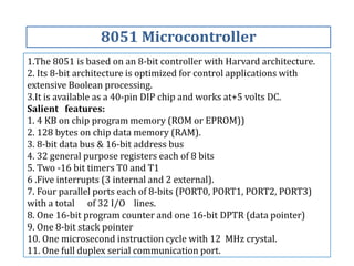
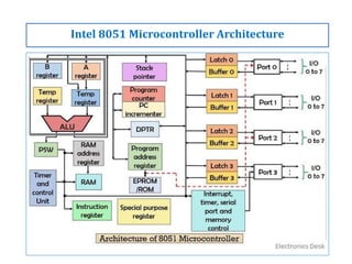
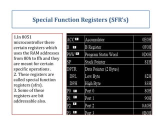
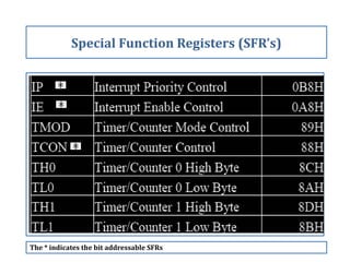
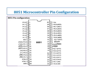
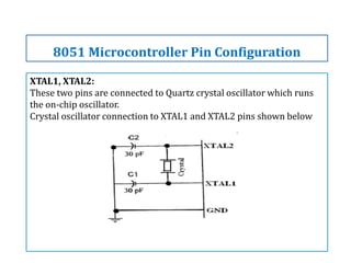
The document discusses the 8051 microcontroller, including its architecture, pins, ports, and memory organization. It provides details on the 8051's 8-bit CPU, registers, program memory, data memory, special function registers, and four 8-bit I/O ports. It also describes the functions of key pins for the crystal oscillator, reset, external access, and program store enable.
2. INTRODUCTION:
8051 microcontroller is one of the most successful controller given by Intel company.
8051 is more convenient to use rather than the microprocessor for a single application
Because it is very cost-effective and it is a system on chip .
Microcntroller-8051
OUTCOMES:
Student understands the architecture of 8051 microcontroller.
Student understands the addressing modes and instruction set of 8051 microcontroller.
Student can develop various assembly language programs in real time applications
Using microcontrollers.
4. What is a Microcontroller?
A single chip computer or A CPU with all the peripherals like RAM,
ROM, I/O Ports, Timers/Counters On the same chip.
For ex: Motorola's 6811, Intel’s 8051, Zilog’s Z8 and PIC 16X etc…
8051 Microcontroller
6. 8051 Microcontroller
1.The 8051 is based on an 8-bit controller with Harvard architecture.
2. Its 8-bit architecture is optimized for control applications with
extensive Boolean processing.
3.It is available as a 40-pin DIP chip and works at+5 volts DC.
Salient features:
1. 4 KB on chip program memory (ROM or EPROM))
2. 128 bytes on chip data memory (RAM).
3. 8-bit data bus & 16-bit address bus
4. 32 general purpose registers each of 8 bits
5. Two -16 bit timers T0 and T1
6 .Five interrupts (3 internal and 2 external).
7. Four parallel ports each of 8-bits (PORT0, PORT1, PORT2, PORT3)
with a total of 32 I/O lines.
8. One 16-bit program counter and one 16-bit DPTR (data pointer)
9. One 8-bit stack pointer
10. One microsecond instruction cycle with 12 MHz crystal.
11. One full duplex serial communication port.
8. 1.8051 has 8-bit ALU which can perform all the 8-bit arithmetic and
logical operations in one machine cycle.
2. The ALU is associated with two registers A & B
A and B Registers:
1.The A and B registers are special function registers which hold the
results of many arithmetic and logical operations of 8051.
2.The A register is also called the Accumulator
3.B register especially used to store the second operand while doing
the multiplication and division operation .
The R registers:
1. The "R" registers are a set of eight registers that are named R0, R1,
up to R7.
2. The "R" registers are also used to temporarily store values. These R
registers and banks are there in the Internal RAM.
Intel 8051 Microcontroller Architecture
9. Program Counter (PC):
1. 8051 has a 16-bit program counter .
2. The program counter always points to the address of the next
instruction to be executed.
Stack Pointer Register (SP):
1. It is an 8-bit register which stores the address of the stack top. i.e the
Stack Pointer is used to indicate where the next value to be removed
from the stack should be taken from.
Data pointer register (DPTR):
1. It is a 16-bit register which is the only user-accessible.
2.DPTR, as the name suggests, is used to point to data.
3. When the 8051 accesses external memory it will access external
memory at the address indicated by DPTR.
4. This DPTR can also be used as two8-registers DPH and DPL.
Intel 8051 Microcontroller Architecture
10. Program Status Word Register (PSW):
1. The 8051 has a 8-bit PSW register which is also known as Flag
register.
2. The two unused bits are user definable bits.
3. In the 6-bits four of them are conditional flags.
PSW Register :
Intel 8051 Microcontroller Architecture
CY AC F0 RS1 RS0 OV F1 P
PSW.7 PSW.6 PSW.5 PSW.4 PSW.3 PSW.2 PSW.1 PSW.0
11. The meaning of various bits of PSW register is shown below:
Intel 8051 Microcontroller Architecture
Name of the flag Bit position Meaning
CY PSW.7 Carry flag
AC PSW.6 Auxiliary carry flag
F0 PSW.5 Flag 0 available for general purpose
RS1 PSW.4 Register bank select bit 1
RS0 PSW.3 Register bank select bit 0
OV PSW.2 Overflow flag
F1 PSW.1 Flag 1 for general purpose
P PSW.0 Parity flag .Set/cleared by hardware
12. The selection of the register banks and their addresses are given below
Intel 8051 Microcontroller Architecture
RS1 RS0 REGISTER BANK ADDRESS
0 0 0 00H - 07H
0 1 1 08H - 0FH
1 0 2 10H - 17H
1 1 3 18H - 1FH
13. 1.The 8051 microcontroller has 128 bytes of internal RAM and 4kb of
on chip ROM .
2. The RAM is also known as data memory and the ROM is known as
program memory.
3. Both RAM & ROM capacity can extend upto 64KB(by interfacing
External memory with 8051)
INTERNAL RAM OF 8051:
1. This internal RAM is found on-chip on the 8051.
2. So it is the fastest RAM available, and it is also the most flexible in
terms of reading, writing, and modifying its contents.
3. Internal RAM is volatile, so when the 8051 is reset this memory is
cleared.
Memory Organization
14. The 128 bytes of internal
RAM is organized as below.
1. Four register banks
(Bank0, Bank1, Bank2 and
Bank3) each of 8-bytes (total
32 bytes). The default bank
register is Bank0.
2. 16 bytes of bit addressable
area
3. 80 bytes of general
purpose area (Scratch pad
memory) as shown in the
diagram .
Memory Organization
Internal RAM organization:
15. Internal ROM (on - chip ROM):
1. The 8051 microcontroller has
4 kB of on chip ROM but it can be
extended up to 64kB.This ROM is
also called program memory or
code memory.
2. The CODE segment is accessed
using the program counter (PC)
for opcode fetches and by DPTR
for data.
3. The external ROM is accessed
when the EA (active low) pin is
connected to ground .
Memory Organization
Internal ROM organization :
16. 1.In 8051
microcontroller there
certain registers which
uses the RAM addresses
from 80h to ffh and they
are meant for certain
specific operations .
2. These registers are
called special function
registers (sfrs).
3. Some of these
registers are bit
addressable also.
Special Function Registers (SFR’s)
18. 1. The 8051 microcontroller has four parallel I/O ports, each of 8-bits .
2. So, it provides the user 32 I/O lines for connecting the
microcontroller to the peripherals.
3. The four ports are P0 (port 0),p1(port1) ,p2(port 2) and P3 (port3).
4. Upon reset all the ports are output ports. In order to make them
input, all the ports must be set i.e a high bit must be sent to all the port
pins.
PORT 0:
1. Port 0 is an 8-bit I/O port with dual purpose.
2. If external memory is used, these port pins are used for the lower
address byte address/data (AD0-AD7), otherwise all bits of the port
are either input or output.
Parallel I /O Ports
19. 3. Unlike other ports, Port 0 is not provided with pull-up resistors
internally, so for PORT0 pull-up resistors of nearly 10k are to be
connected externally as shown in the below fig.
Parallel I /O Ports
20. PORT 1:
1. Port 1 occupies a total of 8 pins (pins 1 through 8).
2. It has no dual application and acts only as input or output port.
3. In contrast to port 0, this port does not need any pull-up resistors
since pull-up resistors connected internally.
PORT 2:
1. Port 2 is also an eight bit parallel port. (Pins 21- 28).
2. It can be used as input or output port.
3. As this port is provided with internal pull-up resistors it does not
need any external pull-up resistors.
4. Port2 lines are also associated with the higher order address lines
A8-A15.
Parallel I /O Ports
21. PORT 3:
1. Port3 is also an 8-bit parallel port
with dual function.( Pins 10 to 17).
2. The port pins can be used for I/O
operations as well as for control
operations.
3. The details of these additional
operations are given in the table.
4. Port 3 also do not need any
external pull-up resistors as they are
provided internally similar to the
case of port2 & port 1.
Parallel I /O Ports
23. XTAL1, XTAL2:
These two pins are connected to Quartz crystal oscillator which runs
the on-chip oscillator.
Crystal oscillator connection to XTAL1 and XTAL2 pins shown below
8051 Microcontroller Pin Configuration
24. RST:
1. The RESET pin is an input pin and it is an active high pin.
2. When a high pulse is applied to this pin the microcontroller will
reset and terminate all activities.
EA (External Access):
1. This pin is an active low pin.
2. This pin is connected to ground when microcontroller is accessing
the program code stored in the external memory and connected to Vcc
when it is accessing the program code in the on chip memory.
PSEN (Program Store Enable):
1. This is an output pin which is active low.
2. When the microcontroller is accessing the program code stored in
the external ROM, this pin is connected to the OE (Output Enable) pin
of the ROM.
ALE (ADDRESS LATCH ENABLE):
1. This ALE pin will de multiplex the address and data bus.
2. When the pin is high, the AD bus will act as address bus otherwise
the AD bus will act as data bus.
8051 Microcontroller Pin Configuration
25. P0.0- P0.7 (AD0-AD7):
The port 0 pins multiplexed with Address/data pins .If the
microcontroller is accessing external memory these pins will act as
address/data pins otherwise they are used for Port 0 pins.
P2.0- P2.7 (A8-A15):
The port2 pins are multiplexed with the higher order address pins.
When the microcontroller is accessing external memory these pins
provide the higher order address byte otherwise they act as Port 2
pins.
P1.0- P1.7:
These 8-pins are dedicated for Port1 to perform input or output port
operations.
P3.0- P3.7:
These 8-pins are meant for Port3 operations and also for some control
operations like Read, Write, Timer0, Timer1, INT0, INT1, RxD and TxD.
8051 Microcontroller Pin Configuration