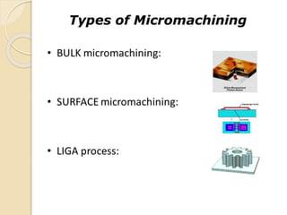
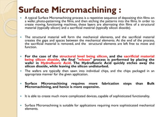
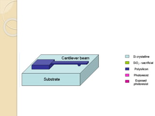
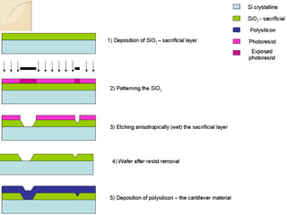
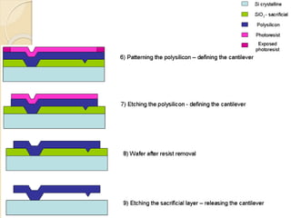
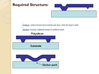
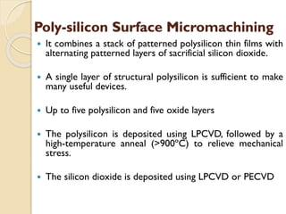
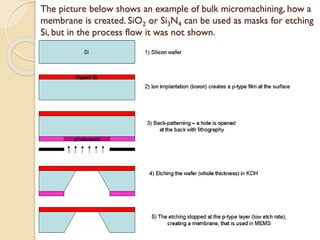
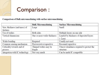
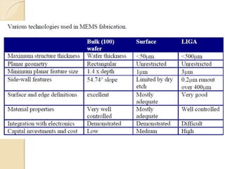
MEMS Micromachining
Chapter 3 - Malluf Book
Fabrication and Manufacturing:
Production of a MEMS device consists of two phases –
Phase 1 - involves the fabrication of structures and elements on the silicon wafer
Phase 2 - involves packaging and assembly of individual silicon chips.
The assembled chip products are mounted on PC Boards for insertion into
electronics systems.
Surface Micromachining :
 Creates structures on top of a substrate
 Features are built up, layer by layer on the
surface of a substrate.
 Uses a succession of thin film deposition
and selective etching
Surface Micromachining :
 A typical Surface Micromachining process is a repetitive sequence of depositing thin films on
a wafer, photo-patterning the films, and then etching the patterns into the films. In order to
create moving, functioning machines, these layers are alternating thin films of a structural
material (typically silicon) and a sacrificial material (typically silicon dioxide).
 The structural material will form the mechanical elements, and the sacrificial material
creates the gaps and spaces between the mechanical elements. At the end of the process,
the sacrificial material is removed, and the structural elements are left free to move and
function.
 For the case of the structural level being silicon, and the sacrificial material
being silicon dioxide, the final "release" process is performed by placing the
wafer in Hydrofluoric Acid. The Hydrofluoric Acid quickly etches away the
silicon dioxide, while leaving the silicon undisturbed.
 The wafers are typically then sawn into individual chips, and the chips packaged in an
appropriate manner for the given application.
 Surface Micromachining requires more fabrication steps than Bulk
Micromachining, and hence is more expensive.
 It is able to create much more complicated devices, capable of sophisticated functionality.
 Surface Micromachining is suitable for applications requiring more sophisticated mechanical
elements.
Required Structure:
Poly-silicon Surface Micromachining
 It combines a stack of patterned polysilicon thin films with
alternating patterned layers of sacrificial silicon dioxide.
 A single layer of structural polysilicon is sufficient to make
many useful devices.
 Up to five polysilicon and five oxide layers
 The polysilicon is deposited using LPCVD, followed by a
high-temperature anneal (>900ºC) to relieve mechanical
stress.
 The silicon dioxide is deposited using LPCVD or PECVD
 Each of the layers in the stack is lithographically
patterned and etched before the next layer is
deposited in order to form the appropriate shapes
and to make provisions for anchor points to the
substrate
 The final release step consists of etching the silicon
dioxide (hence the sacrificial term) in a hydrofluoric
acid solution to free the polysilicon plates and beams.
 Thus allowing motion in the plane of and
perpendicular to the substrate.
Poly-silicon Surface Micromachining
 Surface micromachining offers significant flexibility to fabricate planar
structures one layer at a time, but their thinness limits the applications to
those benefiting from essentially two dimensional forms.
 Polysilicon is a useful structural material because integrated circuit
processes already exist for depositing and etching it.
 Its thermal coefficient of expansion is well matched to that of the silicon
substrate.
 However, surface micromachining is not limited to the materials just
described.
 Many systems of structural layer, sacrificial layer, and etchant have been
used
 Texas Instruments’ Digital Mirror Device™ (DMD™) display
technology uses a surface-micromachined device with
aluminum as its structural element and an organic polymer as
a sacrificial layer
Poly-silicon Surface Micromachining :
Surface Micromachining :
The etchant must etch the sacrificial layer at a useful rate, while having little
or no impact on the structural layer.
Reasons for selecting materials other than polysilicon include the need for
higher electrical conductivity, higher optical reflectivity, and lower
deposition temperature for compatibility with CMOS circuitry that is already
on the wafer.
Bulk micromachining :
Is removal of a lot of material - almost the entire film thickness -
to create windows, membranes, various structures
 Produces structures inside a substrate by selectively etching deeply inside
a substrate
 Substrate include Si, ceramic, plastic or glass materials.
 Usually, Si wafers are used as substrates for bulk
micromachining, as they can be anisotropically wet etched,
forming highly regular structures
 Wet etching typically uses alkaline liquid solvents, such as potassium
hydroxide (KOH) or tetramethylammonium hydroxide (TMAH) to
dissolve silicon which has been left exposed by the photolithography
masking step.
The picture below shows an example of bulk micromachining, how a
membrane is created. SiO2 or Si3N4 can be used as masks for etching
Si, but in the process flow it was not shown.
Bulk Micromachining:
 Bulk micromachining is a fabrication technique which builds mechanical
elements by starting with a silicon wafer, and then etching away unwanted parts,
and being left with useful mechanical devices.
 Typically, the wafer is photo patterned, leaving a protective layer on the parts of
the wafer that you want to keep. The wafer is then submersed into a liquid
etchant, like potassium hydroxide, which eats away any exposed silicon.
 This is a relatively simple and inexpensive fabrication technology, and is
well suited for applications which do not require much complexity, and which
are price sensitive.
 Today, almost all pressure sensors are built with Bulk Micromachining. Bulk
Micromachined pressure sensors offer several advantages over traditional
pressure sensors. They cost less, are highly reliable, manufacturable,
and there is very good repeatability between devices.
 All new cars on the market today have several micromachined pressure
sensors, typically used to measure manifold pressure in the engine.
 The small size and high reliability of micromachined pressure sensors make
them ideal for a variety of medical applications as well.
Comparison :
LIGA : is a German acronym for Lithographie,
Galvanoformung, Abformung (Lithography, Electroplating
and Molding)
 A fabrication technology used to create high-aspect-ratio
microstructures,(structures that are much taller than
wide), popularly known as HAR MEMS.
 There are two main LIGA-fabrication technologies
 X-Ray LIGA, which uses X-ray produced by a synchrotron
to create high-aspect ratio structures.
 UV LIGA, a more accessible method which uses ultraviolet
light to create structures with relatively low aspect ratios.
LIGA :using x-ray lithography
Process flow of LIGA technology:
LIGA :using x-ray lithography
 The process typically starts with a sheet of PMMA (polymethyl-
methacrylate).
 The PMMA is covered with a photomask, and then exposed to high energy x-
rays.
 The mask allows parts of the PMMA to be exposed to the x-rays, while
protecting other parts.
 The PMMA is then placed in a suitable etchant to remove the selected areas.
 Chemical removal of exposed (or unexposed) photoresist results in a three-
dimensional structure, which can be filled by the electrodeposition of metal.
 In the electroplating step, nickel, copper, or gold is plated upward from the
metalized substrate into the voids left by the removed photoresist.
 Taking place in an electrolytic cell, the current density, temperature, and solution
are carefully controlled to ensure proper plating.
 In the case of nickel deposition from NiCl2 in a KCl solution, Ni is deposited on
the cathode (metalized substrate) and Cl2 evolves at the anode.
 Difficulties associated with plating into PMMA molds include voids, where
hydrogen bubbles nucleate on contaminates, chemical incompatibility, where the
plating solution attacks the photoresist, and mechanical incompatibility, where film
stress causes the plated layer to lose adhesion.
 These difficulties can be overcome through the empirical optimization of the
plating chemistry and environment for a given layout.
 Repeat masking, allows parts of the PMMA to be exposed to the x-rays, while
protecting electroplated area.
 Resulting in extremely precise, microscopic mechanical elements.
 LIGA is a relatively inexpensive fabrication technology, and suitable for
applications requiring higher aspect ratio devices than what is achievable in
Surface Micromachining.
LIGA :using x-ray lithography
 High aspect ratios on the order of 100:1
 Parallel side walls with a flank angle on the
order of 89.95°
 Structural heights from tens of micrometers
to several millimetres
 Structural details on the order of
micrometers over distances of centimeters
LIGA :using x-ray lithography
 X-ray mask are expensive
 Mask are made of cobalt
 X-rays has no scattering effect
 PMMA is sensitive to X-rays
LIGA :using x-ray lithography
UV LIGA :
 Uses an inexpensive ultraviolet light source, like a mercury
lamp, to expose a polymer photoresist, typically SU-8.
 Because heating and transmittance are not an issue in
optical masks, a simple chromium mask can be substituted
for the technically sophisticated X-ray mask.
 These reductions in complexity make UV LIGA much
cheaper and more accessible than its X-ray counterpart.
 However, UV LIGA is not as effective at producing precision
molds and is thus used when cost must be kept low and
very high aspect ratios are not required.
 Picture of an ant carrying a LIGA micro gear.
 This picture made the cover of Scientific American Magazine in
November 1992
LIGA Structures :
 SEM picture of a polymer LIGA structure made by moulding.
 Smallest polymer width is 6µm; polymer height is 120µm, the aspect ratio
is, therefore, 20.
LIGA Structures :
LIGA
Structures :
Thank You

MEMS Fabrication Techniques_2024.pdf

  • 1.
  • 2.
    Fabrication and Manufacturing: Productionof a MEMS device consists of two phases – Phase 1 - involves the fabrication of structures and elements on the silicon wafer Phase 2 - involves packaging and assembly of individual silicon chips. The assembled chip products are mounted on PC Boards for insertion into electronics systems.
  • 4.
    Surface Micromachining : Creates structures on top of a substrate  Features are built up, layer by layer on the surface of a substrate.  Uses a succession of thin film deposition and selective etching
  • 7.
    Surface Micromachining : A typical Surface Micromachining process is a repetitive sequence of depositing thin films on a wafer, photo-patterning the films, and then etching the patterns into the films. In order to create moving, functioning machines, these layers are alternating thin films of a structural material (typically silicon) and a sacrificial material (typically silicon dioxide).  The structural material will form the mechanical elements, and the sacrificial material creates the gaps and spaces between the mechanical elements. At the end of the process, the sacrificial material is removed, and the structural elements are left free to move and function.  For the case of the structural level being silicon, and the sacrificial material being silicon dioxide, the final "release" process is performed by placing the wafer in Hydrofluoric Acid. The Hydrofluoric Acid quickly etches away the silicon dioxide, while leaving the silicon undisturbed.  The wafers are typically then sawn into individual chips, and the chips packaged in an appropriate manner for the given application.  Surface Micromachining requires more fabrication steps than Bulk Micromachining, and hence is more expensive.  It is able to create much more complicated devices, capable of sophisticated functionality.  Surface Micromachining is suitable for applications requiring more sophisticated mechanical elements.
  • 11.
  • 12.
    Poly-silicon Surface Micromachining It combines a stack of patterned polysilicon thin films with alternating patterned layers of sacrificial silicon dioxide.  A single layer of structural polysilicon is sufficient to make many useful devices.  Up to five polysilicon and five oxide layers  The polysilicon is deposited using LPCVD, followed by a high-temperature anneal (>900ºC) to relieve mechanical stress.  The silicon dioxide is deposited using LPCVD or PECVD
  • 13.
     Each ofthe layers in the stack is lithographically patterned and etched before the next layer is deposited in order to form the appropriate shapes and to make provisions for anchor points to the substrate  The final release step consists of etching the silicon dioxide (hence the sacrificial term) in a hydrofluoric acid solution to free the polysilicon plates and beams.  Thus allowing motion in the plane of and perpendicular to the substrate. Poly-silicon Surface Micromachining
  • 14.
     Surface micromachiningoffers significant flexibility to fabricate planar structures one layer at a time, but their thinness limits the applications to those benefiting from essentially two dimensional forms.  Polysilicon is a useful structural material because integrated circuit processes already exist for depositing and etching it.  Its thermal coefficient of expansion is well matched to that of the silicon substrate.  However, surface micromachining is not limited to the materials just described.  Many systems of structural layer, sacrificial layer, and etchant have been used  Texas Instruments’ Digital Mirror Device™ (DMD™) display technology uses a surface-micromachined device with aluminum as its structural element and an organic polymer as a sacrificial layer Poly-silicon Surface Micromachining :
  • 15.
    Surface Micromachining : Theetchant must etch the sacrificial layer at a useful rate, while having little or no impact on the structural layer. Reasons for selecting materials other than polysilicon include the need for higher electrical conductivity, higher optical reflectivity, and lower deposition temperature for compatibility with CMOS circuitry that is already on the wafer.
  • 17.
    Bulk micromachining : Isremoval of a lot of material - almost the entire film thickness - to create windows, membranes, various structures  Produces structures inside a substrate by selectively etching deeply inside a substrate  Substrate include Si, ceramic, plastic or glass materials.  Usually, Si wafers are used as substrates for bulk micromachining, as they can be anisotropically wet etched, forming highly regular structures  Wet etching typically uses alkaline liquid solvents, such as potassium hydroxide (KOH) or tetramethylammonium hydroxide (TMAH) to dissolve silicon which has been left exposed by the photolithography masking step.
  • 18.
    The picture belowshows an example of bulk micromachining, how a membrane is created. SiO2 or Si3N4 can be used as masks for etching Si, but in the process flow it was not shown.
  • 19.
    Bulk Micromachining:  Bulkmicromachining is a fabrication technique which builds mechanical elements by starting with a silicon wafer, and then etching away unwanted parts, and being left with useful mechanical devices.  Typically, the wafer is photo patterned, leaving a protective layer on the parts of the wafer that you want to keep. The wafer is then submersed into a liquid etchant, like potassium hydroxide, which eats away any exposed silicon.  This is a relatively simple and inexpensive fabrication technology, and is well suited for applications which do not require much complexity, and which are price sensitive.  Today, almost all pressure sensors are built with Bulk Micromachining. Bulk Micromachined pressure sensors offer several advantages over traditional pressure sensors. They cost less, are highly reliable, manufacturable, and there is very good repeatability between devices.  All new cars on the market today have several micromachined pressure sensors, typically used to measure manifold pressure in the engine.  The small size and high reliability of micromachined pressure sensors make them ideal for a variety of medical applications as well.
  • 20.
  • 21.
    LIGA : isa German acronym for Lithographie, Galvanoformung, Abformung (Lithography, Electroplating and Molding)  A fabrication technology used to create high-aspect-ratio microstructures,(structures that are much taller than wide), popularly known as HAR MEMS.  There are two main LIGA-fabrication technologies  X-Ray LIGA, which uses X-ray produced by a synchrotron to create high-aspect ratio structures.  UV LIGA, a more accessible method which uses ultraviolet light to create structures with relatively low aspect ratios.
  • 22.
    LIGA :using x-raylithography
  • 23.
    Process flow ofLIGA technology:
  • 24.
    LIGA :using x-raylithography  The process typically starts with a sheet of PMMA (polymethyl- methacrylate).  The PMMA is covered with a photomask, and then exposed to high energy x- rays.  The mask allows parts of the PMMA to be exposed to the x-rays, while protecting other parts.  The PMMA is then placed in a suitable etchant to remove the selected areas.  Chemical removal of exposed (or unexposed) photoresist results in a three- dimensional structure, which can be filled by the electrodeposition of metal.  In the electroplating step, nickel, copper, or gold is plated upward from the metalized substrate into the voids left by the removed photoresist.  Taking place in an electrolytic cell, the current density, temperature, and solution are carefully controlled to ensure proper plating.
  • 25.
     In thecase of nickel deposition from NiCl2 in a KCl solution, Ni is deposited on the cathode (metalized substrate) and Cl2 evolves at the anode.  Difficulties associated with plating into PMMA molds include voids, where hydrogen bubbles nucleate on contaminates, chemical incompatibility, where the plating solution attacks the photoresist, and mechanical incompatibility, where film stress causes the plated layer to lose adhesion.  These difficulties can be overcome through the empirical optimization of the plating chemistry and environment for a given layout.  Repeat masking, allows parts of the PMMA to be exposed to the x-rays, while protecting electroplated area.  Resulting in extremely precise, microscopic mechanical elements.  LIGA is a relatively inexpensive fabrication technology, and suitable for applications requiring higher aspect ratio devices than what is achievable in Surface Micromachining. LIGA :using x-ray lithography
  • 26.
     High aspectratios on the order of 100:1  Parallel side walls with a flank angle on the order of 89.95°  Structural heights from tens of micrometers to several millimetres  Structural details on the order of micrometers over distances of centimeters LIGA :using x-ray lithography
  • 27.
     X-ray maskare expensive  Mask are made of cobalt  X-rays has no scattering effect  PMMA is sensitive to X-rays LIGA :using x-ray lithography
  • 28.
    UV LIGA : Uses an inexpensive ultraviolet light source, like a mercury lamp, to expose a polymer photoresist, typically SU-8.  Because heating and transmittance are not an issue in optical masks, a simple chromium mask can be substituted for the technically sophisticated X-ray mask.  These reductions in complexity make UV LIGA much cheaper and more accessible than its X-ray counterpart.  However, UV LIGA is not as effective at producing precision molds and is thus used when cost must be kept low and very high aspect ratios are not required.
  • 29.
     Picture ofan ant carrying a LIGA micro gear.  This picture made the cover of Scientific American Magazine in November 1992 LIGA Structures :
  • 30.
     SEM pictureof a polymer LIGA structure made by moulding.  Smallest polymer width is 6µm; polymer height is 120µm, the aspect ratio is, therefore, 20. LIGA Structures :
  • 31.
  • 33.