Micro Machining
Machining ofmicro parts is not literally correct.
Removal of material in the form of chips or debris having
the size in the range of microns.
Creating micro features or surface characteristics
(especially surface finish) in the micro/nano level.
Definition: material removal at micro/nano level with no
constraint on the size of the component being machined.
3.
Why Micro Machining?
Finalfinishing operations in manufacturing of precise parts are always of
concern owing to their most critical, labour intensive and least
controllable nature.
In the era of nanotechnology, deterministic high precision finishing
methods are of utmost importance and are the need of present
manufacturing scenario.
The need for high precision in manufacturing was felt by manufacturers
worldwide to improve interchangeability of components, improve quality
control and longer wear/fatigue life.
4.
Why Micro Machining?
Presentday High-tech Industries, Design requirements are stringent.
– Extraordinary Properties of Materials (High Strength, High heat
Resistant, High hardness, Corrosion resistant etc)
– Complex 3D Components (Turbine Blades)
– Miniature Features (filters for food processing and textile industries
having few tens of microns as hole diameter and thousands in number)
– Nano level surface finish on Complex geometries (thousands of
turbulated cooling holes in a turbine blade)
– Making and finishing of micro fluidic channels (in electrically
conducting & non conducting materials, say glass, quartz, &ceramics)
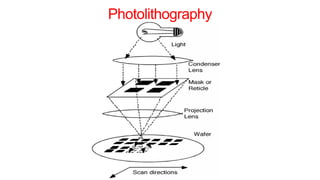
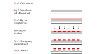
Photolithography Process
Description
• Thewafersare chemically cleaned to remove particulate matter, organic, ionic, and
metallic impurities
• High-speed centrifugal whirling of silicon wafers known as"Spin Coating" producesa
thin uniform layer of photoresist (a light sensitive polymer) on the wafers
• Photoresist is exposedto a set of lights through a maskoftenmade of quartz
• Wavelength of light rangesfrom 300-500 nm (UV) andX-rays (wavelengths 4-50
Angstroms)
• Two types of photoresist areused:
– Positive: whatever shows,goes
– Negative: whatever shows,stays
10.
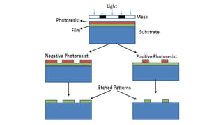
Etching
• Etching isusedin micro fabrication to chemically
remove layers from the surfaceof a wafer during
manufacturing.
• Etching is a critically important process module,
and every wafer undergoesmany etching steps
before it iscomplete.
• It is characterized by etch rate, etch selectivity and
etch uniformity
11.
Process Variations:
1. Wetetching
• Etching processesusedliquid-phase ("wet") etchants. Thewafer can be
immersed in a bath of etchant, which must be agitated toachieve good
processcontrol. Forinstance, buffered hydrofluoric acid (BHF)is used
commonly to etch silicon dioxide over a siliconsubstrate.
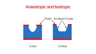
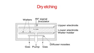
2. Dryetching
• Modern VLSIprocessesavoid wet etching, and useplasma etching
instead. plasma etching operates between 0.1 and 5Torr
• Theplasma produces energetic free radicals, neutrally charged, that
react at the surface of the wafer. Sinceneutral particles attack the
wafer from all angles, this processisisotropic
StepsIn Wet Etching
•Injection of hole into semiconductor tosi+
state
• Attaching –vecharge oh group to positive
charge Si
• Reaction between hydrated Siand complex
agent in etchantsolution
• Dissolution of reactionproduct
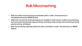
Bulk Micromachinig
• Bulkand surface micromachining are processesusedto create microstructures on
microelectromechanical MEMSdevices.
• While both wet and dry etching techniques are available to both bulk and surface micromachining,
bulk micromachining typically useswet etching techniques while surface micromachining primarily
usesdry etching techniques.
• Bulk micromachining selectively etches the silicon substrate to create microstructures on MEMS
devices.
16.
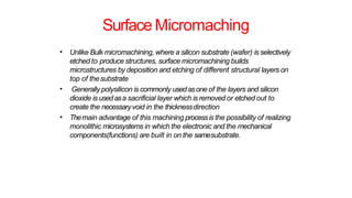
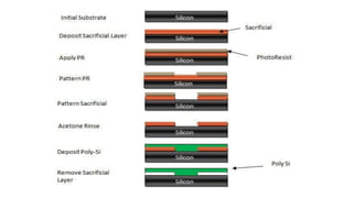
Surface Micromaching
• UnlikeBulk micromachining, where a silicon substrate (wafer) is selectively
etched to produce structures, surface micromachining builds
microstructures by deposition and etching of different structural layers on
top of thesubstrate
Generally polysilicon is commonly usedasone of the layers and silicon
dioxide is usedasa sacrificial layer which is removed or etched out to
create the necessaryvoid in the thicknessdirection
Themain advantage of this machining processis the possibility of realizing
monolithic microsystems in which the electronic and the mechanical
components(functions) are built in on the samesubstrate.
•
•
18.
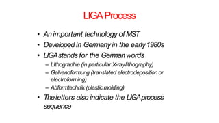
LIGAProcess
• Animportant technologyof MST
• Developed in Germanyin the early1980s
• LIGAstands for the Germanwords
– LIthographie (in particular X-raylithography)
– Galvanoformung (translated electrodeposition or
electroforming)
– Abformtechnik (plastic molding)
• Theletters also indicate the LIGAprocess
sequence
19.
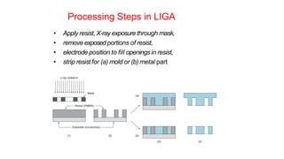
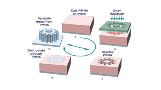
• Apply resist,X-ray exposure through mask,
• remove exposedportions of resist,
• electrode position to fill openings in resist,
• strip resist for (a) mold or (b) metal part
Processing Steps in LIGA
20.
Processsteps
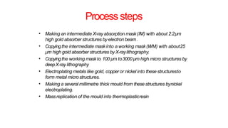
• Making anintermediate X-rayabsorption mask(IM) with about 2.2µm
high gold absorber structures by electron beam.
Copyingthe intermediate maskinto a working mask(WM) with about25
µm high gold absorber structures by X-raylithography.
Copyingthe working maskto 100 µm to3000 µm high micro structures by
deepX-ray lithography
Electroplating metals like gold, copper or nickel into these structuresto
form metal microstructures.
Making a several millimetre thick mould from these structures bynickel
electroplating.
Massreplication of the mould into thermoplasticresin
•
•
•
•
•
22.
Advantages of LIGA
•LIGAis a versatile process– it canproduce
parts by several different methods
• High aspect ratios are possible (largeheight-
to-width ratios in the fabricatedpart)
• Wide range of part sizesis feasible -heights
ranging from micrometers tocentimeters
• Closetolerances are possible
23.
Disadvantages of LIGA
•LIGAis a very expensive process
– Large quantities of parts are usually required tojustify
its application
• LIGAusesX-ray exposure
– Human health hazard