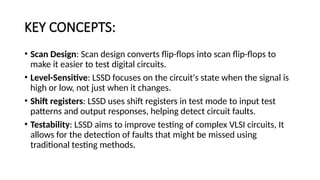
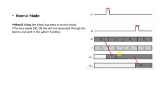
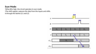
LSSD
(Level-Sensitive Scan Design)
• Is a design-for-testability (DFT) methodology used in VLSI (Very Large
Scale Integration) design.
• It's particularly effective for ensuring the testability of digital circuits,
allowing for testing and debugging of integrated circuits (ICs).
LSSD scan latch is called : Shift Register
Latch(SRL)
KEY CONCEPTS:
• Scan Design: Scan design converts flip-flops into scan flip-flops to
make it easier to test digital circuits.
• Level-Sensitive: LSSD focuses on the circuit's state when the signal is
high or low, not just when it changes.
• Shift registers: LSSD uses shift registers in test mode to input test
patterns and output responses, helping detect circuit faults.
• Testability: LSSD aims to improve testing of complex VLSI circuits, It
allows for the detection of faults that might be missed using
traditional testing methods.
Shift register latches used in LSSD:
Explanation:
• Inputs: D, A, B are the data inputs to the latches.
B0 This is a control input that determines the mode of operation
• Latches:
1. Master 2 port D-latch L1
2. Slave Latch L2
• Outputs: 1.To system function: This is the output that goes to the normal
system operation.
2. S0: This is the scan output, which is used during the testing
phase to shift out the data.
• Normal Mode:
•When B is low, the circuit operates in normal mode.
•The data inputs (D0, C0, Sin, A0) are processed through the
latches and sent to the system function.
Scan Mode:
•When B is high, the circuit operates in scan mode.
•The shift register captures the data from the inputs and shifts
it through the latches (L1 and L2).

LSSD Level-Sensitive Scan Design VLSI ECE 6th Sem

  • 1.
    LSSD (Level-Sensitive Scan Design) •Is a design-for-testability (DFT) methodology used in VLSI (Very Large Scale Integration) design. • It's particularly effective for ensuring the testability of digital circuits, allowing for testing and debugging of integrated circuits (ICs). LSSD scan latch is called : Shift Register Latch(SRL)
  • 2.
    KEY CONCEPTS: • ScanDesign: Scan design converts flip-flops into scan flip-flops to make it easier to test digital circuits. • Level-Sensitive: LSSD focuses on the circuit's state when the signal is high or low, not just when it changes. • Shift registers: LSSD uses shift registers in test mode to input test patterns and output responses, helping detect circuit faults. • Testability: LSSD aims to improve testing of complex VLSI circuits, It allows for the detection of faults that might be missed using traditional testing methods.
  • 3.
  • 4.
    Explanation: • Inputs: D,A, B are the data inputs to the latches. B0 This is a control input that determines the mode of operation • Latches: 1. Master 2 port D-latch L1 2. Slave Latch L2 • Outputs: 1.To system function: This is the output that goes to the normal system operation. 2. S0: This is the scan output, which is used during the testing phase to shift out the data.
  • 5.
    • Normal Mode: •WhenB is low, the circuit operates in normal mode. •The data inputs (D0, C0, Sin, A0) are processed through the latches and sent to the system function.
  • 6.
    Scan Mode: •When Bis high, the circuit operates in scan mode. •The shift register captures the data from the inputs and shifts it through the latches (L1 and L2).

Editor's Notes

  • #1 Now here in this design we going to use latches instead of flipflops, because the flipflops are edge-triggered , changing state only when the control signal transitions from high or low, whereas latches are level- triggered and respond immediately to input changes
  • #2 Test mode :it works for the certain range of PVT( process , voltage and temperature) within the specified range, Shift registers: it is a sequential circuit which stores and transfers the binary data
  • #3 L1: This represents the first stage of the shift register.L2: This represents the second stage of the shift register. Sin: The scan input for feeding test patterns into the shift register.So: The scan output where the test patterns are shifted out. Here one latch is responsible for capturing data during the scan operation. And its consists of multiple NAND and NOT gates arranged to control the flow of data based on the control signals. 2. The latch takes the output from the L1 and further process it. It consists of of combinational of NAND and NOT for controlling data flow.
  • #4 B0 determine the mode of operation whether it is normal mode or scan mode. When B0= 0(low), it works in normal mode When B0= 1(high), its works in scan mode
  • #5 Consider two input clocks: c and b. Let c be the master latch clock and b be the slave latch clock. When the master clock c goes high, the data becomes active and is stored in the master latch, +L1. When the slave clock b goes high, the data from the master latch +L1 is transferred and stored in the slave latch, +L2.
  • #6 Consider two input clocks: ‘a’ and ‘b’. Let ‘a’ be the master latch clock and ‘b’ be the slave latch clock. When the master clock ‘a’ goes high, the data becomes active and is stored in the master latch, +L1. When the slave clock ‘b’ goes high, the data from the master latch +L1 is transferred and stored in the slave latch, +L2.