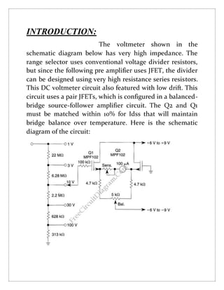
Low drift high impedance
JFET DC voltmeter
Submitted by:
Mafaz Ahmed 1882/FET/BSEE/F12
INTRODUCTION:
The voltmeter shown in the
schematic diagram below has very high impedance. The
range selector uses conventional voltage divider resistors,
but since the following pre amplifier uses JFET, the divider
can be designed using very high resistance series resistors.
This DC voltmeter circuit also featured with low drift. This
circuit uses a pair JFETs, which is configured in a balanced-
bridge source-follower amplifier circuit. The Q2 and Q1
must be matched within 10% for Idss that will maintain
bridge balance over temperature. Here is the schematic
diagram of the circuit:
What is a JFET?
A JFET, or junction gate field-effect transistor, is a type of field-effect
transistor. A JFET can be used as a voltage-controlled resistance or as an
electronically-controlled switch. A p-type JFET consists of a channel of
semiconductor material containing a large amount of positive charge
carriers or holes, whereas an n-type JFET consists of a channel of
semiconductor material containing a large amount of negative charge
carriers or holes. At each end of the JFET, ohmic contacts form the
source and drain. Electric charge flows through the channel between the
source and drain. Electric current can be impeded or switched off by
applying a reverse bias voltage to a gate.
Applicationsfor JFETs:
JFETs can be used for several applications including:
 • High Input Impedance Amplifier
 • Low-Noise Amplifier
 • Differential Amplifier
 • Constant Current Source
 • Analog Switch or Gate
 • Voltage Controlled Resistor
Components
 Sensor
 Voltmeter
 JFET
 Resisters 22M,6.28M,2.2M,628K,
 313K,100K,5K,4.7K
Simulation:
As shown in the simulation above the JFET used is of very high input
impedance. For that high resistances are used in voltage divider circuit. The
potentiometerRV1 is used to balance the circuit.

Low drift high impedance jfet dc voltmeter

  • 1.
    Low drift highimpedance JFET DC voltmeter Submitted by: Mafaz Ahmed 1882/FET/BSEE/F12
  • 2.
    INTRODUCTION: The voltmeter shownin the schematic diagram below has very high impedance. The range selector uses conventional voltage divider resistors, but since the following pre amplifier uses JFET, the divider can be designed using very high resistance series resistors. This DC voltmeter circuit also featured with low drift. This circuit uses a pair JFETs, which is configured in a balanced- bridge source-follower amplifier circuit. The Q2 and Q1 must be matched within 10% for Idss that will maintain bridge balance over temperature. Here is the schematic diagram of the circuit:
  • 3.
    What is aJFET? A JFET, or junction gate field-effect transistor, is a type of field-effect transistor. A JFET can be used as a voltage-controlled resistance or as an electronically-controlled switch. A p-type JFET consists of a channel of semiconductor material containing a large amount of positive charge carriers or holes, whereas an n-type JFET consists of a channel of semiconductor material containing a large amount of negative charge carriers or holes. At each end of the JFET, ohmic contacts form the source and drain. Electric charge flows through the channel between the source and drain. Electric current can be impeded or switched off by applying a reverse bias voltage to a gate. Applicationsfor JFETs: JFETs can be used for several applications including:  • High Input Impedance Amplifier  • Low-Noise Amplifier  • Differential Amplifier  • Constant Current Source  • Analog Switch or Gate  • Voltage Controlled Resistor Components  Sensor  Voltmeter  JFET  Resisters 22M,6.28M,2.2M,628K,  313K,100K,5K,4.7K
  • 4.
    Simulation: As shown inthe simulation above the JFET used is of very high input impedance. For that high resistances are used in voltage divider circuit. The potentiometerRV1 is used to balance the circuit.