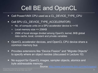
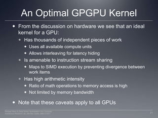
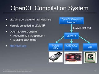
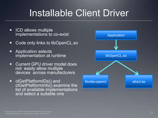
Downloaded 285 times

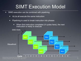
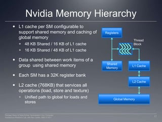
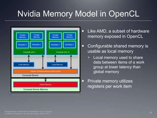
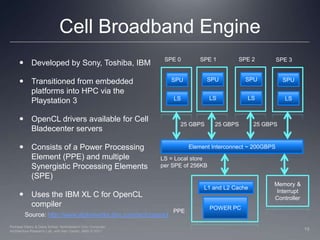

This document provides a high-level overview of GPU architecture, AMD and Nvidia GPU hardware, the OpenCL compilation system, and the installable client driver (ICD). It contrasts conventional CPU and GPU architectures, describes the SIMD and SIMT execution models, and examines key aspects of AMD's VLIW and Nvidia's scalar architectures like memory hierarchies and how they map to the OpenCL memory model. It stresses that understanding hardware can help optimize OpenCL code and provides guidelines for writing optimal GPU kernels.