Download as PDF, PPTX


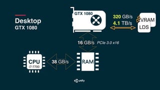


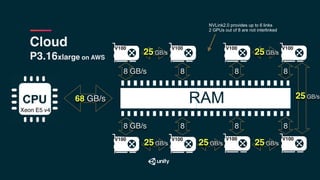


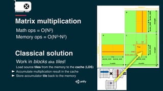


The document discusses the architecture differences between CPUs and GPUs, emphasizing the significant impact of raw TFLOPS on the speed of training convolutional neural networks. It highlights the importance of parallel processing with threads, memory access patterns, and the efficiency of operations such as matrix multiplication in achieving optimal performance. The text also contrasts programming models and memory bandwidth in multi-GPU setups, asserting that the efficiency of data transfers and access plays a crucial role in machine learning computations.