Download to read offline


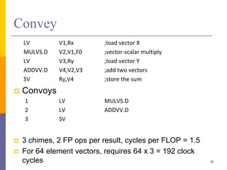
![3. Vector Mask Registers
for (i = 0; i < 64; i=i+1)
if (X[i] != 0)
X[i] = X[i] – Y[i];
Use vector mask register to “disable” elements
LV V1,Rx ;load vector X into V1
LV V2,Ry ;load vector Y
L.D F0,#0 ;load FP zero into F0
SNEVS.D V1,F0 ;sets VM(i) to 1 if V1(i)!=F0
SUBVV.D V1,V1,V2 ;subtract under vector mask
SV Rx,V1 ;store the result in X
20](https://image.slidesharecdn.com/05-data-levelparallelism-240416110633-a9e374da/85/Data-Level-Parallelism-in-Microprocessors-20-320.jpg)

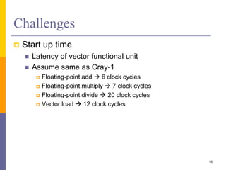
![5. Stride
for (i = 0; i < 100; i=i+1)
for (j = 0; j < 100; j = j+1) {
A[i][j] = 0.0;
for (k = 0; k < 100; k=k+1)
A[i][j] = A[i][j] + B[i][k] * D[k][j];
}
}
Row-major vs. column-major
Vectorize multiplication of rows of B with columns of D
Use non-unit stride
Bank conflict (stall) occurs when same bank is hit faster
than bank busy time
22](https://image.slidesharecdn.com/05-data-levelparallelism-240416110633-a9e374da/85/Data-Level-Parallelism-in-Microprocessors-22-320.jpg)


1. The document discusses data-level parallelism and summarizes vector architectures, SIMD instruction sets, and graphics processing units (GPUs). 2. It describes vector architectures like VMIPS that can perform operations on sets of data elements via vector registers. 3. It also explains how SIMD extensions like SSE exploit fine-grained data parallelism and how GPUs are optimized for data-parallel applications through a multithreaded SIMD execution model.