Download as PDF, PPTX


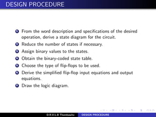

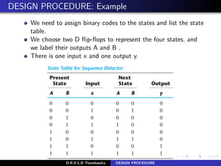


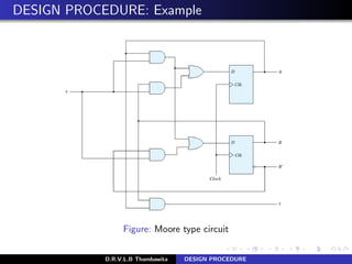

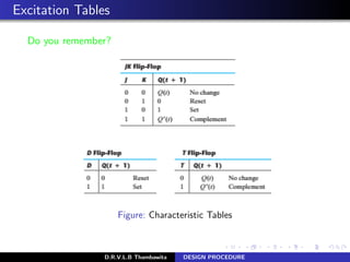


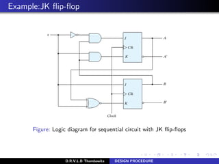
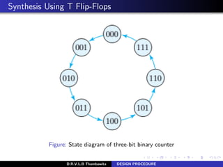
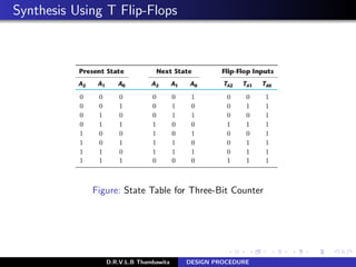


The document outlines the design procedures for clocked sequential circuits, starting from specifications to creating logic diagrams. It emphasizes the importance of deriving state tables or diagrams and covers step-by-step processes including state reduction, binary assignment, and obtaining flip-flop input equations. Additionally, it provides examples and discusses excitation tables for different types of flip-flops used in circuit design.


![Cd2 [autosaved]](https://cdn.slidesharecdn.com/ss_thumbnails/cd2autosaved-161231072301-thumbnail.jpg?width=640&height=640&fit=bounds)

![Reduction of multiple subsystem [compatibility mode]](https://cdn.slidesharecdn.com/ss_thumbnails/reductionofmultiplesubsystemcompatibilitymode-110418075355-phpapp01-thumbnail.jpg?width=640&height=640&fit=bounds)