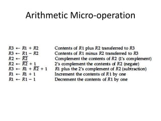
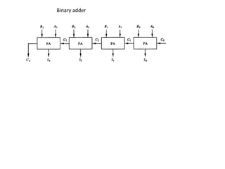
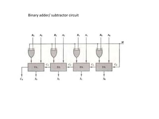
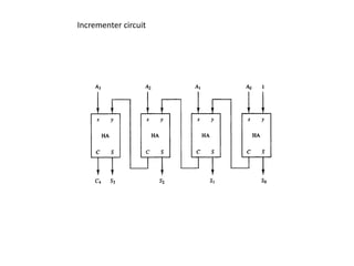
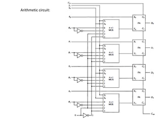
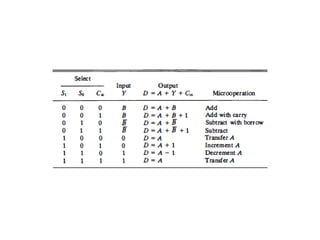
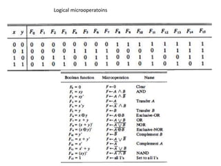
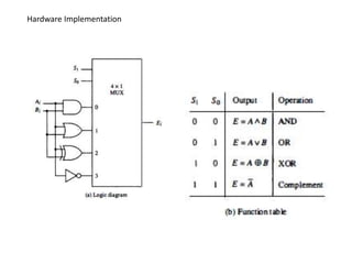
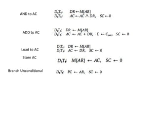
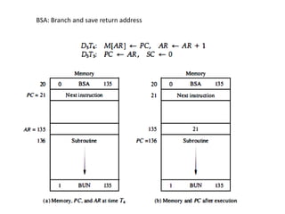
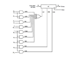
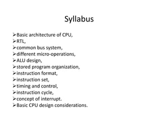
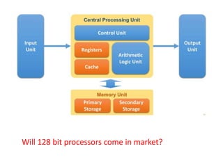
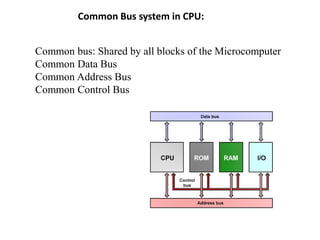
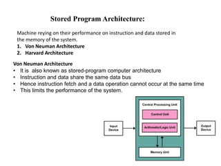
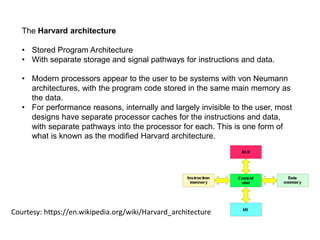
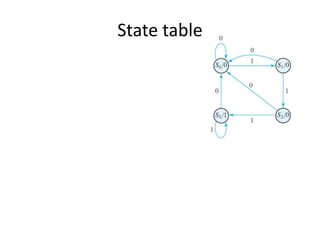
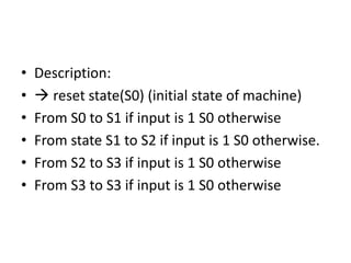
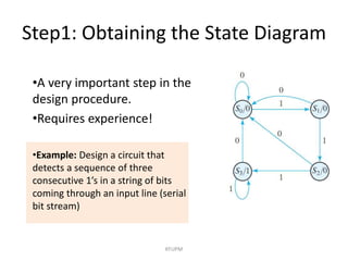
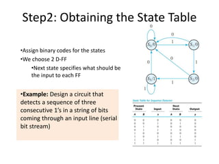
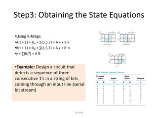
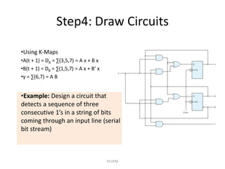
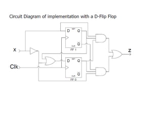
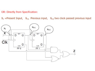
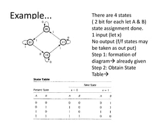
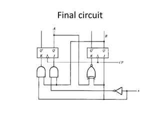
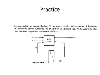
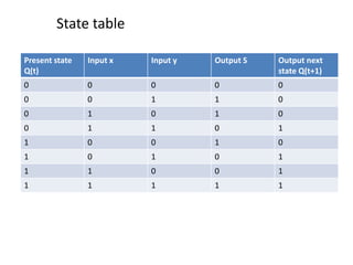
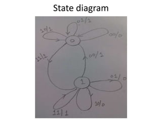
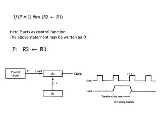
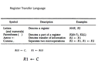
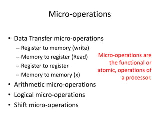
The document details the syllabus for a course on computer design and applications, focusing on CPU architecture, micro-operations, instruction formats, and sequential circuit design. It explains concepts such as von Neumann and Harvard architectures, the implementation of common bus systems, state reduction techniques, and design procedures for sequential circuits. Additionally, it provides design examples for circuits that detect specific patterns in bit streams and various types of counters.


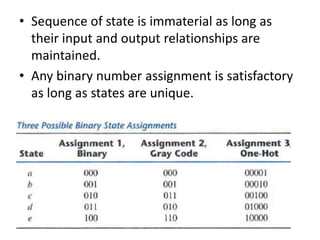


![Memory transfer
• Memory Read:
• CPU put address on address bus, [AR is address Register]
• activate control line [Memory read],
• data comes out of memory and kept on data bus and
transferred to CPU [DR is data Register]](https://image.slidesharecdn.com/uniticda-1-240502190800-90bb6728/85/Unit-I_CDA-1-computer-design-and-applications-102-320.jpg)
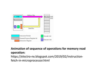
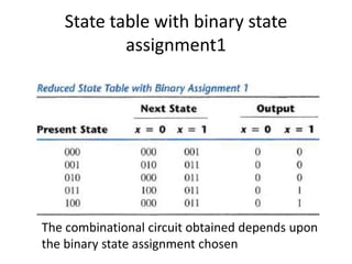
![Memory transfer
• Memory Read: DR M[AR]
• CPU put address on address bus,
• activate control line [Memory Read],
• Put data on data bus
• Save into DR (activate load input of DR)](https://image.slidesharecdn.com/uniticda-1-240502190800-90bb6728/85/Unit-I_CDA-1-computer-design-and-applications-104-320.jpg)