Download to read offline


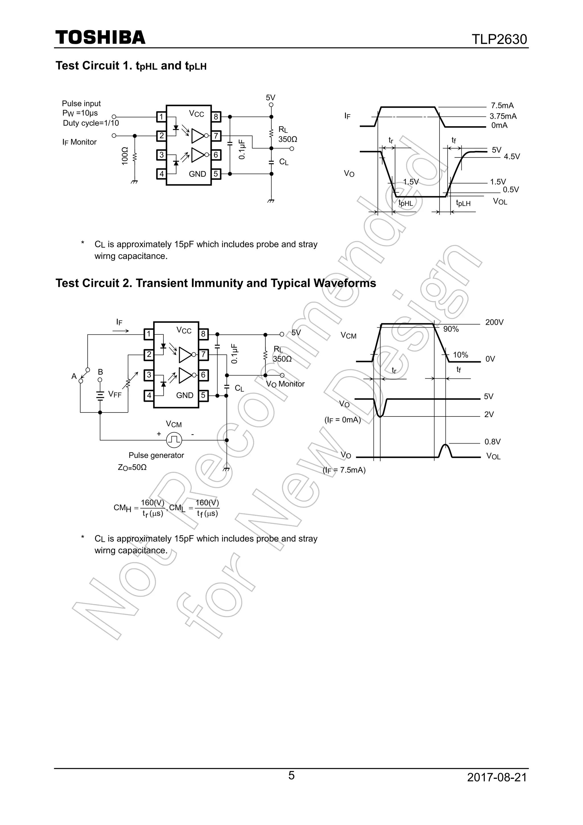
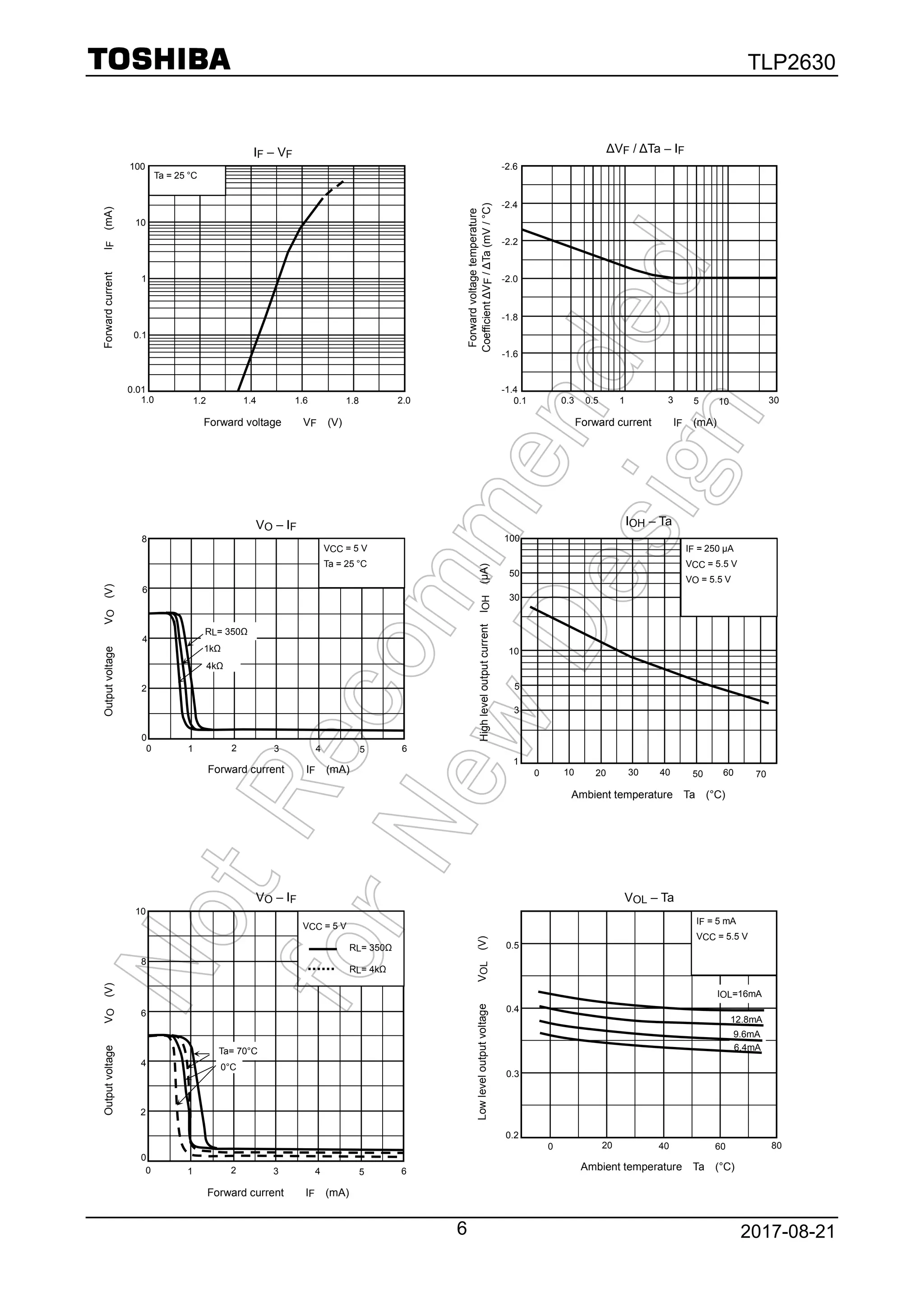
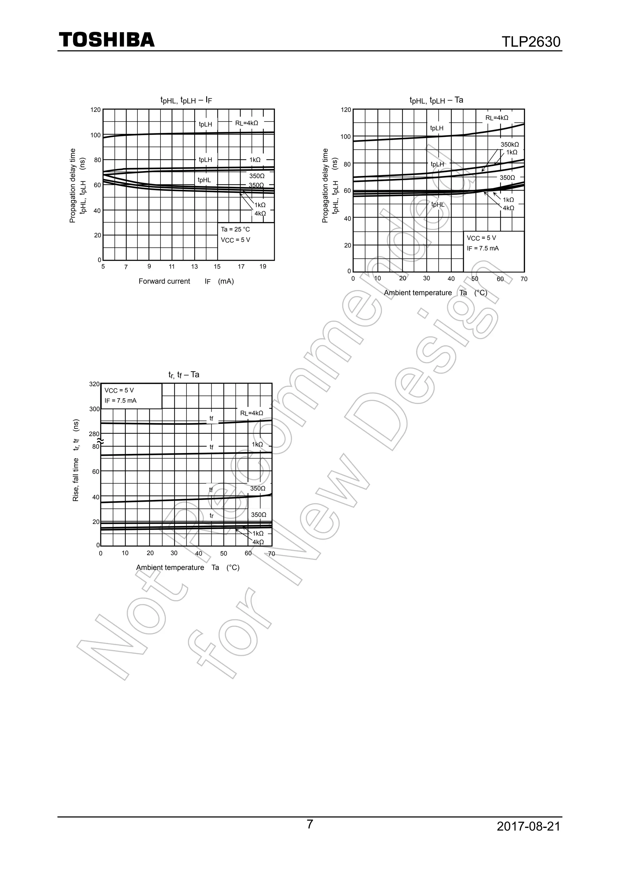


This document provides information on the TLP2630 dual photocoupler from Toshiba consisting of a pair of GaAlAs LEDs and integrated photodetectors. It contains specifications for the electrical characteristics and switching performance including input/output ratings, isolation voltage, propagation delay and transient immunity. The document also includes application information, recommended operating conditions, test circuits and derating curves.


