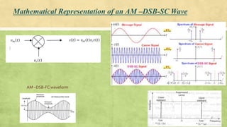
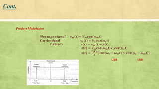
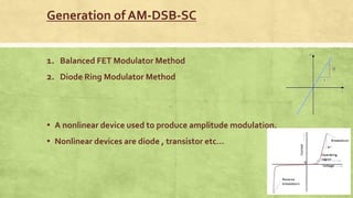
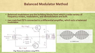
EC8491-Communication Theory
Dr.Arun Chokkalingam
Professor
 Mathematical Representation of AM –DSB-SC Wave
 Generation of AM-DSB-SC using Balanced FET Modulator
Amplitude Modulation(AM)
Mathematical Representation of an AM –DSB-SC Wave
AM –DSB-FC waveform
Cont.
Product Modulation
𝑴𝒆𝒔𝒔𝒂𝒈𝒆 𝒔𝒊𝒈𝒏𝒂𝒍 𝒗𝒎 𝒕 = 𝑽𝒎𝒄𝒐𝒔 𝝎𝒎𝒕
Carrier signal 𝒗𝒄 𝒕 = 𝑽𝒄𝒄𝒐𝒔 𝝎𝒄𝒕
DSB-SC- 𝒔 𝒕 = 𝒗𝒎 𝒕 𝒗𝒄𝒕 𝒕
𝒔 𝒕 = 𝑽𝒎𝒄𝒐𝒔 𝝎𝒎𝒕 𝑽𝒄𝒄𝒐𝒔 𝝎𝒄𝒕
𝒔 𝒕 =
𝑽𝒄𝑽𝒎
𝟐
𝒄𝒐𝒔 𝝎𝒄 + 𝝎𝒎𝒕 + 𝒄𝒐𝒔 𝝎𝒄 − 𝝎𝒎𝒕
USB LSB
Generation of AM-DSB-SC
1. Balanced FET Modulator Method
2. Diode Ring Modulator Method
▪ A nonlinear device used to produce amplitude modulation.
▪ Nonlinear devices are diode , transistor etc…
Balanced Modulator Method
▪ Balanced modulators are the building blocks from which a wide variety of
frequency mixers, modulators, and demodulators are built.
▪ two matched FETs connected in a differential amplifier, which acts a balanced
modulator
𝑣𝑐 + 𝑣𝑚
𝑣𝑐 − 𝑣𝑚
Operation
▪ Carrier voltage is applied in phase to the two gates of FET
▪ Modulating signal appears 1800out of phase at the gate.This is because of input transformerT1 is
a center tapped transformer.
▪ Mode -1 (only carrier signal applied and message signal =0)
▪ Both FETs conduct simultaneously due to the in phase carrier voltage applied to their gates
▪ Their drain currents are equal in magnitude but opposite in direction and cancel each other .The
net output is Zero.
▪ Mode =2 (both carrier and message signal both present)
▪ The drain currents of the two FETs flow due to the combined effect of carrier and message
signal.
▪ The current due to message are equal but not opposite so they do not cancel out.
Cont .
▪ 𝒗𝒈𝒔𝟏 = 𝒗𝒄 + 𝒗𝒎 (1.36)
▪ 𝒗𝒈𝒔𝟐 = 𝒗𝒄 − 𝒗𝒎 (1.37)
▪ 𝒊𝒅𝟏 = 𝑰𝟎 + 𝒂𝒗𝒈𝒔𝟏 + 𝒃𝒗𝒈𝒔𝟏
𝟐
(1.38)
▪ 𝒊𝒅𝟐 = 𝑰𝟎 + 𝒂𝒗𝒈𝒔𝟐 + 𝒃𝒗𝒈𝒔𝟐
𝟐
(1.39)
▪ 𝒊𝒑 = 𝒊𝒅𝟏 − 𝒊𝒅𝟐 (1.40)
▪ Use (1.38) and (1.39) in (1.40), we get,
▪ 𝒊𝒑 = 𝟐𝒂 𝒗𝒎 + 𝟒𝒃 𝒗𝒄 𝒗𝒎 (1.41)
▪ Substitute 𝒗𝒎 = 𝑽𝒎𝒄𝒐𝒔 𝝎𝒎𝒕 and 𝒗𝒄 = 𝑽𝒄𝒄𝒐𝒔 𝝎𝒄𝒕 in equation (1.41) we get,
▪ 𝒊𝒑 = 𝟐𝒂𝑽𝒎𝒄𝒐𝒔 𝝎𝒎𝒕 + 𝟐𝒃𝑽𝒎𝑽𝒄 𝒄𝒐𝒔 𝝎𝒄 − 𝝎𝒎 𝒕 + 𝒄𝒐𝒔 𝝎𝒄 + 𝝎𝒎 𝒕 (1.42)
▪ 𝒗𝟎 ∝ 𝒊𝒑 (1.43)
Disadvantages of FET balanced modulator
▪ 100% of carrier suppression is not possible .
▪ Because both FETs must have the identical characteristics and the
transformer center taps must be exactly at the center of the
windings.
▪ Carrier will be heavily suppressed but not completely removed.
Generation of AM-DSB-SC using Balanced FET Modulator.pptx

Generation of AM-DSB-SC using Balanced FET Modulator.pptx

  • 1.
    EC8491-Communication Theory Dr.Arun Chokkalingam Professor Mathematical Representation of AM –DSB-SC Wave  Generation of AM-DSB-SC using Balanced FET Modulator Amplitude Modulation(AM)
  • 2.
    Mathematical Representation ofan AM –DSB-SC Wave AM –DSB-FC waveform
  • 3.
    Cont. Product Modulation 𝑴𝒆𝒔𝒔𝒂𝒈𝒆 𝒔𝒊𝒈𝒏𝒂𝒍𝒗𝒎 𝒕 = 𝑽𝒎𝒄𝒐𝒔 𝝎𝒎𝒕 Carrier signal 𝒗𝒄 𝒕 = 𝑽𝒄𝒄𝒐𝒔 𝝎𝒄𝒕 DSB-SC- 𝒔 𝒕 = 𝒗𝒎 𝒕 𝒗𝒄𝒕 𝒕 𝒔 𝒕 = 𝑽𝒎𝒄𝒐𝒔 𝝎𝒎𝒕 𝑽𝒄𝒄𝒐𝒔 𝝎𝒄𝒕 𝒔 𝒕 = 𝑽𝒄𝑽𝒎 𝟐 𝒄𝒐𝒔 𝝎𝒄 + 𝝎𝒎𝒕 + 𝒄𝒐𝒔 𝝎𝒄 − 𝝎𝒎𝒕 USB LSB
  • 4.
    Generation of AM-DSB-SC 1.Balanced FET Modulator Method 2. Diode Ring Modulator Method ▪ A nonlinear device used to produce amplitude modulation. ▪ Nonlinear devices are diode , transistor etc…
  • 5.
    Balanced Modulator Method ▪Balanced modulators are the building blocks from which a wide variety of frequency mixers, modulators, and demodulators are built. ▪ two matched FETs connected in a differential amplifier, which acts a balanced modulator 𝑣𝑐 + 𝑣𝑚 𝑣𝑐 − 𝑣𝑚
  • 6.
    Operation ▪ Carrier voltageis applied in phase to the two gates of FET ▪ Modulating signal appears 1800out of phase at the gate.This is because of input transformerT1 is a center tapped transformer. ▪ Mode -1 (only carrier signal applied and message signal =0) ▪ Both FETs conduct simultaneously due to the in phase carrier voltage applied to their gates ▪ Their drain currents are equal in magnitude but opposite in direction and cancel each other .The net output is Zero. ▪ Mode =2 (both carrier and message signal both present) ▪ The drain currents of the two FETs flow due to the combined effect of carrier and message signal. ▪ The current due to message are equal but not opposite so they do not cancel out.
  • 7.
    Cont . ▪ 𝒗𝒈𝒔𝟏= 𝒗𝒄 + 𝒗𝒎 (1.36) ▪ 𝒗𝒈𝒔𝟐 = 𝒗𝒄 − 𝒗𝒎 (1.37) ▪ 𝒊𝒅𝟏 = 𝑰𝟎 + 𝒂𝒗𝒈𝒔𝟏 + 𝒃𝒗𝒈𝒔𝟏 𝟐 (1.38) ▪ 𝒊𝒅𝟐 = 𝑰𝟎 + 𝒂𝒗𝒈𝒔𝟐 + 𝒃𝒗𝒈𝒔𝟐 𝟐 (1.39) ▪ 𝒊𝒑 = 𝒊𝒅𝟏 − 𝒊𝒅𝟐 (1.40) ▪ Use (1.38) and (1.39) in (1.40), we get, ▪ 𝒊𝒑 = 𝟐𝒂 𝒗𝒎 + 𝟒𝒃 𝒗𝒄 𝒗𝒎 (1.41) ▪ Substitute 𝒗𝒎 = 𝑽𝒎𝒄𝒐𝒔 𝝎𝒎𝒕 and 𝒗𝒄 = 𝑽𝒄𝒄𝒐𝒔 𝝎𝒄𝒕 in equation (1.41) we get, ▪ 𝒊𝒑 = 𝟐𝒂𝑽𝒎𝒄𝒐𝒔 𝝎𝒎𝒕 + 𝟐𝒃𝑽𝒎𝑽𝒄 𝒄𝒐𝒔 𝝎𝒄 − 𝝎𝒎 𝒕 + 𝒄𝒐𝒔 𝝎𝒄 + 𝝎𝒎 𝒕 (1.42) ▪ 𝒗𝟎 ∝ 𝒊𝒑 (1.43)
  • 8.
    Disadvantages of FETbalanced modulator ▪ 100% of carrier suppression is not possible . ▪ Because both FETs must have the identical characteristics and the transformer center taps must be exactly at the center of the windings. ▪ Carrier will be heavily suppressed but not completely removed.