InvenSense ICM-20789: High Performance 6-Axis Motion Sensor and Pressure Sensor Combo 2017 teardown reverse costing report published by Yole Developpement

World’s first ‘7-Axis’ motion tracking device targeting drone application Having supplied Apple for many years, InvenSense (TDK) is a leader in the inertial measurement unit (IMU) market. It has a large market share, competing with Bosch and others. This year, with the acquisition of Sensirion’s barometric pressure sensor division, InvenSense has entered a new market area. It has now released of its first ‘7-axis’ motion tracking combo, bringing together a 6-axis IMU and a pressure sensor, moving it into drone applications. The ICM-20789 7-axis combo sensor released by InvenSense features a 6-axis device, incorporating a 3-axis gyroscope and a 3-axis accelerometer, and a barometric pressure sensor previously developed by Sensirion in the same package. Compared with the stand-alone sensor hub, this approach eliminates a package and minimizes board area requirements. More information on that report at http://www.i-micronews.com/reports.html

Recommended
More Related Content
What's hot
What's hot (20)
Similar to InvenSense ICM-20789: High Performance 6-Axis Motion Sensor and Pressure Sensor Combo 2017 teardown reverse costing report published by Yole Developpement
Similar to InvenSense ICM-20789: High Performance 6-Axis Motion Sensor and Pressure Sensor Combo 2017 teardown reverse costing report published by Yole Developpement (20)
More from Yole Developpement
More from Yole Developpement (20)
Recently uploaded
Recently uploaded (20)
InvenSense ICM-20789: High Performance 6-Axis Motion Sensor and Pressure Sensor Combo 2017 teardown reverse costing report published by Yole Developpement
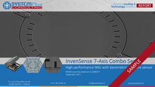
- 1. ©2017 System Plus Consulting | InvenSense ICM-20789 7-Axis Combo Sensor 1 21 rue la Noue Bras de Fer 44200 NANTES - FRANCE +33 2 40 18 09 16 info@systemplus.fr www.systemplus.fr InvenSense 7-Axis Combo Sensor High performance IMU with barometric pressure sensor MEMS report by Stéphane ELISABETH September 2017
- 2. ©2017 System Plus Consulting | InvenSense ICM-20789 7-Axis Combo Sensor 2 Table of Contents Overview / Introduction 3 o Executive Summary o Reverse Costing Methodology Company Profile 6 o InvenSense Physical Analysis 11 o Synthesis of the Physical Analysis o Physical Analysis Methodology o Package 14 Package Views & Dimensions Package Opening Wire Bonding Process Package Cross-Section o Pressure Sensor Die 23 View & Dimensions Details Views Deprocessing & Marking Delayering & Main Block ID Process Cross-Section (Substrate, Metal Pad, Cavity, TSVs) o ASIC/MEMS Die 56 View, Dimensions & Marking MEMS Removed o MEMS Die 62 MEMS Sensing Area Detailed MEMS Gyroscope & Accelerometer MEMS Cap o ASIC Die 92 Overview Delayering & Main Blocks ID Die Process Cross-Section (ASIC, Sensor, Cap & Sealing) Process Characteristics Physical Comparison with MP67B, ICM-30630 & iPhone 7 Plus OIS IMU 121 Manufacturing Process Flow 127 o Global Overview o Pressure Sensor ASIC Front-End Process o Pressure Sensor ASIC Wafer Fabrication Unit o Pressure Sensor MEMS Process Flow o IMU ASIC Front-End Process o IMU MEMS/ASIC Wafer Fabrication Unit o IMU MEMS Process Flow o Packaging Process Flow o Package Assembly Unit Cost Analysis 148 o Synthesis of the cost analysis o Yields Explanation & Hypotheses o IMU MEMS/ASIC Die 153 ASIC Front-End Cost MEMS Front-End Cost ASIC/MEMS Assembly Cost MEMS Front-End Cost per process steps Total Front-End Cost ASIC/MEMS Back-End 0 : Probe Test & Dicing Wafer & Die Cost o Pressure Sensor Die 161 ASIC Front-End Cost MEMS Front-End Cost MEMS Front-End Cost per process steps Total Front-End Cost ASIC/MEMS Back-End 0 : Probe Test & Dicing Wafer & Die Cost o Component 168 Back-End : Packaging Cost Back-End : Final Test Cost Component Cost Estimated Price Analysis 172 Company services 176
- 3. ©2017 System Plus Consulting | InvenSense ICM-20789 7-Axis Combo Sensor 3 Overview / Introduction o Executive Summary o Reverse Costing Methodology Company Profile & Supply Chain Physical Analysis Physical Comparison Manufacturing Process Flow Cost Analysis Selling Price Analysis About System Plus Executive Summary • This full reverse costing study has been conducted to provide insight on technology data, manufacturing cost and selling price of the ICM-20789 7-Axis Combo Sensor supplied by InvenSense. • The ICM-20789 7-axis combo sensor released by InvenSense features a 6-axis device, incorporating a 3-axis gyroscope and a 3-axis accelerometer, and a barometric pressure sensor previously developed by Sensirion in the same package. Compared with the stand-alone sensor hub, this approach eliminates a package and minimizes board area requirements. • The pressure sensor’s MEMS capacitive architecture provides the industry’s lowest noise at the lowest power. Combined with the motion-tracking 6-axis inertial sensor in a small footprint, the device is ideal for a wide range of motion tracking applications. • The inertial MEMS sensor is fabricated with a minimal number of masks and is directly assembled on the application-specific integrated circuit (ASIC) by eutectic bonding. Using knowledge obtained by acquiring Sensirion’s pressure sensor division, InvenSense was able to design its own pressure sensor. The device is shipped in a 4 mm x 4 mm x 1.37 mm land grid array (LGA) package. • This report includes a detailed technology and cost analysis of the ICM-20789 7-axis motion tracking device. A comparison with the previous generation of combo sensors from InvenSense is also included in the report.
- 4. ©2017 System Plus Consulting | InvenSense ICM-20789 7-Axis Combo Sensor 4 Overview / Introduction o Executive Summary o Reverse Costing Methodology Company Profile & Supply Chain Physical Analysis Physical Comparison Manufacturing Process Flow Cost Analysis Selling Price Analysis About System Plus The reverse costing analysis is conducted in 3 phases: Teardown analysis • Package is analyzed and measured • The dies are extracted in order to get overall data: dimensions, main blocks, pad number and pin out, die marking • Setup of the manufacturing process. Costing analysis • Setup of the manufacturing environment • Cost simulation of the process steps Selling price analysis • Supply chain analysis • Analysis of the selling price Reverse Costing Methodology
- 5. ©2017 System Plus Consulting | InvenSense ICM-20789 7-Axis Combo Sensor 5 Overview / Introduction Company Profile & Supply Chain Physical Analysis o Synthesis o Package o Pressure Sensor Die o PS Die Cross-Section o ASIC/MEMS Die o MEMS Die o ASIC Die o ASIC/MEMS Cross-Section Physical Comparison Manufacturing Process Flow Cost Analysis Selling Price Analysis About System Plus Synthesis of the Physical Analysis
- 6. ©2017 System Plus Consulting | InvenSense ICM-20789 7-Axis Combo Sensor 6 Overview / Introduction Company Profile & Supply Chain Physical Analysis o Synthesis o Package o Pressure Sensor Die o PS Die Cross-Section o ASIC/MEMS Die o MEMS Die o ASIC Die o ASIC/MEMS Cross-Section Physical Comparison Manufacturing Process Flow Cost Analysis Selling Price Analysis About System Plus Package View & Dimensions 4.0 mm 4.0mm1.37mm • Package: LGA 24-pin • Dimensions: 4.0 x 4.0 x 1.37 mm • Pin Pitch: 0.5 mm • Marking: IC2789E AK559LA1 1722 Package Top View ©2017 by System Plus Consulting Package Bottom View ©2017 by System Plus Consulting Package Side View ©2017 by System Plus Consulting
- 7. ©2017 System Plus Consulting | InvenSense ICM-20789 7-Axis Combo Sensor 7 Overview / Introduction Company Profile & Supply Chain Physical Analysis o Synthesis o Package o Pressure Sensor Die o PS Die Cross-Section o ASIC/MEMS Die o MEMS Die o ASIC Die o ASIC/MEMS Cross-Section Physical Comparison Manufacturing Process Flow Cost Analysis Selling Price Analysis About System Plus Package Opening
- 8. ©2017 System Plus Consulting | InvenSense ICM-20789 7-Axis Combo Sensor 8 Overview / Introduction Company Profile & Supply Chain Physical Analysis o Synthesis o Package o Pressure Sensor Die o PS Die Cross-Section o ASIC/MEMS Die o MEMS Die o ASIC Die o ASIC/MEMS Cross-Section Physical Comparison Manufacturing Process Flow Cost Analysis Selling Price Analysis About System Plus Package Cross-Section
- 9. ©2017 System Plus Consulting | InvenSense ICM-20789 7-Axis Combo Sensor 9 Overview / Introduction Company Profile & Supply Chain Physical Analysis o Synthesis o Package o Pressure Sensor Die o PS Die Cross-Section o ASIC/MEMS Die o MEMS Die o ASIC Die o ASIC/MEMS Cross-Section Physical Comparison Manufacturing Process Flow Cost Analysis Selling Price Analysis About System Plus Pressure Sensor – Die View & Dimensions
- 10. ©2017 System Plus Consulting | InvenSense ICM-20789 7-Axis Combo Sensor 10 Overview / Introduction Company Profile & Supply Chain Physical Analysis o Synthesis o Package o Pressure Sensor Die o PS Die Cross-Section o ASIC/MEMS Die o MEMS Die o ASIC Die o ASIC/MEMS Cross-Section Physical Comparison Manufacturing Process Flow Cost Analysis Selling Price Analysis About System Plus Pressure Sensor – Die Details
- 11. ©2017 System Plus Consulting | InvenSense ICM-20789 7-Axis Combo Sensor 11 Overview / Introduction Company Profile & Supply Chain Physical Analysis o Synthesis o Package o Pressure Sensor Die o PS Die Cross-Section o ASIC/MEMS Die o MEMS Die o ASIC Die o ASIC/MEMS Cross-Section Physical Comparison Manufacturing Process Flow Cost Analysis Selling Price Analysis About System Plus Pressure Sensor – Die Cross-Section – TSVs
- 12. ©2017 System Plus Consulting | InvenSense ICM-20789 7-Axis Combo Sensor 12 Overview / Introduction Company Profile & Supply Chain Physical Analysis o Synthesis o Package o Pressure Sensor Die o PS Die Cross-Section o ASIC/MEMS Die o MEMS Die o ASIC Die o ASIC/MEMS Cross-Section Physical Comparison Manufacturing Process Flow Cost Analysis Selling Price Analysis About System Plus Pressure Sensor – Die Cross-Section – Sensor
- 13. ©2017 System Plus Consulting | InvenSense ICM-20789 7-Axis Combo Sensor 13 Overview / Introduction Company Profile & Supply Chain Physical Analysis o Synthesis o Package o Pressure Sensor Die o PS Die Cross-Section o ASIC/MEMS Die o MEMS Die o ASIC Die o ASIC/MEMS Cross-Section Physical Comparison Manufacturing Process Flow Cost Analysis Selling Price Analysis About System Plus IMU 6-Axis – Die View & Dimensions
- 14. ©2017 System Plus Consulting | InvenSense ICM-20789 7-Axis Combo Sensor 14 Overview / Introduction Company Profile & Supply Chain Physical Analysis o Synthesis o Package o Pressure Sensor Die o PS Die Cross-Section o ASIC/MEMS Die o MEMS Die o ASIC Die o ASIC/MEMS Cross-Section Physical Comparison Manufacturing Process Flow Cost Analysis Selling Price Analysis About System Plus IMU 6-Axis – MEMS Sensing Area – Gyroscope
- 15. ©2017 System Plus Consulting | InvenSense ICM-20789 7-Axis Combo Sensor 15 Overview / Introduction Company Profile & Supply Chain Physical Analysis o Synthesis o Package o Pressure Sensor Die o PS Die Cross-Section o ASIC/MEMS Die o MEMS Die o ASIC Die o ASIC/MEMS Cross-Section Physical Comparison Manufacturing Process Flow Cost Analysis Selling Price Analysis About System Plus MEMS Die Cross-Section – Sealing
- 16. ©2017 System Plus Consulting | InvenSense ICM-20789 7-Axis Combo Sensor 16 Overview / Introduction Company Profile & Supply Chain Physical Analysis Physical Comparison o Package o ASIC Die o MEMS Die Manufacturing Process Flow Cost Analysis Selling Price Analysis About System Plus Comparison with MP67B, ICM-30630 & 6-Axis IMU in iPhone 7 Plus
- 17. ©2017 System Plus Consulting | InvenSense ICM-20789 7-Axis Combo Sensor 17 Overview / Introduction Company Profile & Supply Chain Physical Analysis Physical Comparison Manufacturing Process Flow o Global Overview o Pressure Sensor Process o ASIC Front-End Process o MEMS Front-End Process o Packaging Process Cost Analysis Selling Price Analysis About System Plus Pressure Sensor MEMS/ASIC Front-End Process Flow
- 18. ©2017 System Plus Consulting | InvenSense ICM-20789 7-Axis Combo Sensor 18 Overview / Introduction Company Profile & Supply Chain Physical Analysis Physical Comparison Manufacturing Process Flow o Global Overview o Pressure Sensor Process o ASIC Front-End Process o MEMS Front-End Process o Packaging Process Cost Analysis Selling Price Analysis About System Plus Pressure Sensor MEMS – Sensor Process Flow 1/3
- 19. ©2017 System Plus Consulting | InvenSense ICM-20789 7-Axis Combo Sensor 19 Overview / Introduction Company Profile & Supply Chain Physical Analysis Physical Comparison Manufacturing Process Flow o Global Overview o Pressure Sensor Process o ASIC Front-End Process o MEMS Front-End Process o Packaging Process Cost Analysis Selling Price Analysis About System Plus MEMS Front-End Process Flow
- 20. ©2017 System Plus Consulting | InvenSense ICM-20789 7-Axis Combo Sensor 20 Overview / Introduction Company Profile & Supply Chain Physical Analysis Physical Comparison Manufacturing Process Flow Cost Analysis o Synthesis o Supply Chain o Yields o ASIC/MEMS Wafer & Die Cost o Pressure sensor Wafer & Die Cost o Back-End Cost o Component Cost Selling Price Analysis About System Plus ASIC/MEMS Wafer & Die Cost
- 21. ©2017 System Plus Consulting | InvenSense ICM-20789 7-Axis Combo Sensor 21 Overview / Introduction Company Profile & Supply Chain Physical Analysis Physical Comparison Manufacturing Process Flow Cost Analysis o Synthesis o Supply Chain o Yields o ASIC/MEMS Wafer & Die Cost o Pressure sensor Wafer & Die Cost o Back-End Cost o Component Cost Selling Price Analysis About System Plus Pressure Sensor ASIC Front-End Cost
- 22. ©2017 System Plus Consulting | InvenSense ICM-20789 7-Axis Combo Sensor 22 Overview / Introduction Company Profile & Supply Chain Physical Analysis Physical Comparison Manufacturing Process Flow Cost Analysis o Synthesis o Supply Chain o Yields o ASIC/MEMS Wafer & Die Cost o Pressure sensor Wafer & Die Cost o Back-End Cost o Component Cost Selling Price Analysis About System Plus Pressure Sensor Wafer & Die Cost
- 23. ©2017 System Plus Consulting | InvenSense ICM-20789 7-Axis Combo Sensor 23 Overview / Introduction Company Profile & Supply Chain Physical Analysis Physical Comparison Manufacturing Process Flow Cost Analysis o Synthesis o Supply Chain o Yields o ASIC/MEMS Wafer & Die Cost o Pressure sensor Wafer & Die Cost o Back-End Cost o Component Cost Selling Price Analysis About System Plus Component Cost
- 24. ©2017 System Plus Consulting | InvenSense ICM-20789 7-Axis Combo Sensor 24 Overview / Introduction Company Profile & Supply Chain Physical Analysis Physical Comparison Manufacturing Process Flow Cost Analysis Selling Price Analysis o Financial Ratios o Manufacturer Price About System Plus InvenSense 7-Axis Combo Sensor Estimated Manufacturer Price
- 25. COMPLETE TEARDOWN WITH: • Detailed photos • Precise measurements • Material analysis • Manufacturing process flow • Supply chain evaluation • Manufacturing cost analysis • Estimated sales price • Comparison between InvenSense’s previous custom IMUs in the iPhone 7, in the iPhone 6S and the ICM-30630 device InvenSense ICM-20789: High Performance 6-Axis Motion Sensor and Pressure Sensor Combo Title: InvenSense ICM- 20789 – 7-Axis Combo Pages: 175 Date: October 2017 Format: PDF & Excel file Price: Full report: EUR 3,490 World’s first ‘7-Axis’ motion tracking device targeting drone applications together a 6-axis IMU and a pressure sensor, moving it into drone applications. The ICM-20789 7-axis combo sensor released by InvenSense features a 6-axis device, incorporating a 3-axis gyroscope and a 3-axis accelerometer, and a barometric pressure sensor previously developed by Sensirion in the same package. Compared with the stand-alone sensor hub, this approach eliminates a package and minimizes board area requirements. The pressure sensor’s MEMS capacitive architecture provides the industry’s lowest noise at the lowest power. Combined with the motion-tracking 6-axis inertial sensor in a small footprint, the device is ideal for a wide range of motion tracking applications. The inertial MEMS sensor is fabricated with a minimal number of masks and is directly assembled on the application-specific integrated circuit (ASIC) by eutectic bonding. Using knowledge obtained by acquiring Sensirion’s pressure sensor division, InvenSense was able to design its own pressure sensor. The device is shipped in a 4 mm x 4 mm x 1.37 mm land grid array (LGA) package. This report includes a detailed technology and cost analysis of the ICM-20789 7-axis motion tracking device. A comparison with the previous generation of combo sensors from InvenSense is also included in the report. Having supplied Apple for many years, InvenSense (TDK) is a leader in the inertial measurement unit (IMU) market. It has a large market share, competing with Bosch and others. This year, with the acquisition of Sensirion’s barometric pressure sensor division, InvenSense has entered a new market area. It has now released of its first ‘7-axis’ motion tracking combo, bringing
- 26. TABLE OF CONTENTS Overview / Introduction Company Profile and Supply Chain Physical Analysis • Package Package views and dimensions, opening and cross-section • Pressure Sensor Die View, dimensions, and marking Delayering and process Cross-section • MEMS Die View, dimensions and marking Cap removed Sensing area Cross-sections of the sensor, cap, and seal • ASIC Die View, dimensions, and marking Delayering and process Cross-section Manufacturing Process Flow • ASIC front-end process and wafer fabrication unit • Pressure sensor process flow and wafer fabrication unit • MEMS process flow and wafer fabrication unit • Packaging process flow and assembly unit Cost Analysis • Yield hypotheses • Pressure sensor front-end cost • Pressure sensor back-end 0: probe test and dicing • Pressure sensor front-end cost per process steps • Pressure sensor wafer and die cost • ASIC front-end cost • ASIC back-end 0: probe test and dicing • ASIC wafer and die cost • MEMS front-end cost • MEMS back-end 0: probe test and dicing • MEMS front-end cost per process steps • MEMS wafer and die cost • Back-end: packaging cost • Back-end: packaging cost per process steps • Back-end: final test cost • IMU component cost Estimated Price Analysis Comparison with InvenSense IMU MP-67B, Sensor Hub ICM- 30360 and iPhone 7 Plus OIS IMU Performed by AUTHORS: ANALYSIS PERFORMED WITH OUR COSTING TOOLS MEMS COSIM+ AND IC PRICE+ MEMS CoSim+ IC Price+ System Plus Consulting offers powerful costing tools to evaluate the production cost and selling price from single chip to complex structures. MEMS Cosim+ Cost simulation tool to evaluate the cost of any MEMS process or device: From single chip to complex structures. IC Price+ The tool performs the necessary cost simulation of any Integrated Circuit: ASICs, microcontrollers, DSP, memories, smartpower… to set up its laboratory. He previously worked at Atmel Nantes Technological Analysis Laboratory and at Hirex Engineering in Toulouse. Yvon Le Goff (Lab) Yvon joined System Plus Consulting in 2011 Stéphane Elisabeth Stéphane has a deep knowledge of materials characterizations and electronics systems. He holds an Engineering Degree in Electronics and Numerical Technology, and a PhD in Materials for Micro-electronics. previously worked in micro- electronics R&D for CEA/LETI in Grenoble and for STMicro- electronics in Crolles. Nicolas Radufe (Lab) Nicolas is in charge of physical analysis. He Distributed by
- 27. ANNUAL SUBSCRIPTION OFFER You can choose to buy over 12 months a set of 3, 4, 5, 7, 10 or 15 Reverse Costing® reports. Up to 47% discount! • MEMS & Sensors: Accelerometer - Compass - Display / Optics - Environment - Fingerprint - Gyroscope - IMU/Combo - Light - Microphone - Oscillator - Pressure sensor • Power: GaN - IGBT - MOSFET - Si Diode - SiC • Systems: Automotive - Consumer - Energy - Medical - Telecom Each year System Plus Consulting releases a comprehensive collection of new reverse engineering & costing analyses in various domains. • Imaging: Infrared - Visible • Integrated Circuits & RF: Integrated Circuit (IC) - RF IC • LEDs: LED Lamp - UV LED - White/blue LED • Packaging: 3D Packaging - Embedded - SIP - WLP More than 60 reports released each year on the following topics (considered for 2017): Performed by RELATED REPORTS 6-Axis OIS IMUs: STMicroelectronics LSM6DSM 6-Axis OIS IMUs: InvenSense IMU in iPhone 7 Plus Bosch BME680 Environmental Sensor with Integrated Gas Sensor STMicroelectronics has released the LSM6DSM, providing a smaller device with a footprint of 2.5x3mm. In the iPhone 7 Plus, Apple uses a new custom version of the InvenSense ICM-20600 in a 3x3mm 16-pin package compared to a 2.5x3mm 14-pin package. The world's first environmental sensor combining gas, pressure, humidity and temperature sensing functions in a 3mm x 3mm footprint package. Pages: 136 Date: December 2016 Full report: EUR 3,290* Pages: 155 Date: December 2016 Full report: EUR 3,290* Pages: 152 Date: July 2017 Full report: EUR 3,490* Bundle of 2 reports + detailed comparison: EUR 5,500* Distributed by
- 28. ORDER FORM Please process my order for “InvenSense ICM-20789 – 7-Axis Combo” Reverse Costing Report Full Reverse Costing report: EUR 3,490* Ref.: SP17361 *For price in dollars please use the day’s exchange rate. All reports are delivered electronically in pdf format. For French customer, add 20 % for VAT. Performed by DELIVERY on receipt of payment: By credit card: Number: |__|__|__|__| |__|__|__|__| |__|__|__|__| |__|__|__|__| Expiration date: |__|__|/|__|__| Card Verification Value: |__|__|__| By bank transfer: BANK INFO: HSBC, 1 place de la Bourse, F-69002 Lyon, France, Bank code : 30056, Branch code : 00170 Account No : 0170 200 1565 87, SWIFT or BIC code : CCFRFRPP, IBAN : FR76 3005 6001 7001 7020 0156 587 Return order by: • FAX: +33 (0)472 83 01 83 • MAIL: YOLE DEVELOPPEMENT, 75 Cours Emile Zola, F - 69100 Lyon - Villeurbanne Contact: • Japan: Miho - Ohtake@yole.fr • Greater China: Mavis - Wang@yole.fr • Asia: Takashi - Onozawa@yole.fr • EMEA: Lizzie - Levenez@yole.fr • North America: Steve – laferriere@yole.fr • General: info@yole.fr The present document is valid till November 15, 2017 SHIP TO PAYMENT BILLING CONTACT ABOUT YOLE DEVELOPPEMENT Name (Mr/Ms/Dr/Pr): ...................................................................................... Job Title: ...................................................................................... Company: ...................................................................................... Address: ...................................................................................... City: State: ...................................................................................... Postcode/Zip: ...................................................................................... Country: ...................................................................................... VAT ID Number for EU members: ...................................................................................... Tel: ...................................................................................... Email: ..................................................................................... Date: ....................................................................................... Signature: ...................................................................................... Distributed by First Name: .................................................................. Last Name: ............................................................................ Email:............................................................................ Phone:..................................................................................... Founded in 1998, Yole Développement has grown to become a group of companies providing marketing, technology and strategy consulting, media and corporate finance services. With a strong focus on emerging applications using silicon and/or micro manufacturing, the Yole Développement group has expanded to include more than 50 collaborators worldwide covering MEMS, Compound Semiconductors, LED, Image Sensors, Optoelectronics, Microfluidics & Medical, Advanced Packaging, Manufacturing, Nanomaterials, Power Electronics and Batteries & Energy Management. The “More than Moore” company Yole, along with its partners System Plus Consulting, Blumorpho and KnowMade, support industrial companies, investors and R&D organizations worldwide to help them understand markets and follow technology trends to grow their business. CUSTOM STUDIES • Market data & research, marketing analysis • Technology analysis • Reverse engineering & costing services • Strategy consulting • Patent analysis More information on www.yole.fr MEDIA • i-Micronews.com, online disruptive technologies website and its weekly e- newsletter, @Micronews • Communication & webcasts services • Events: Yole Seminars, Market Briefings More information on http://www.i-micronews.com/media-kit.html TECHNOLOGY & MARKET REPORTS • Collection of technology & market reports • Manufacturing cost simulation tools • Component reverse engineering & costing analysis • Patent investigation More information on http://www.i- micronews.com/reports.html
- 29. Performed by TERMS AND CONDITIONS OF SALES . Definitions: “Acceptance”: Action by which the Buyer accepts the terms and conditions of sale in their entirety. It is done by signing the purchase order which mentions “I hereby accept Yole’s Terms and Conditions of Sale”. “Buyer”: Any business user (i.e. any person acting in the course of its business activities, for its business needs) entering into the following general conditions to the exclusion of consumers acting in their personal interests. “Contracting Parties” or “Parties”: The Seller on the one hand and the Buyer on the other hand. “Intellectual Property Rights” (“IPR”) means any rights held by the Seller in its Products, including any patents, trademarks, registered models, designs, copyrights, inventions, commercial secrets and know-how, technical information, company or trading names and any other intellectual property rights or similar in any part of the world, notwithstanding the fact that they have been registered or not and including any pending registration of one of the above mentioned rights. “License”: For the reports and databases, 3 different licenses are proposed. The buyer has to choose one license: • One user license: one person at the company can use the report. • Multi-user license: the report can be used by unlimited users within the company. Subsidiaries and Joint-Ventures are not included. • Corporate license: purchased under “Annual Subscription” program, the report can be used by unlimited users within the company. Joint-Ventures are not included. “Products”: Depending on the purchase order, reports or database on MEMS, CSC, Optics/MOEMS, Nano, bio… to be bought either on a unit basis or as an annual subscription. (i.e. subscription for a period of 12 calendar months). The annual subscription to a package (i.e. a global discount based on the number of reports that the Buyer orders or accesses via the service, a global search service on line on I-micronews and a consulting approach), is defined in the order. Reports are established in PowerPoint and delivered on a PDF format and the database may include Excel files. “Seller”: Based in Lyon (France headquarters), Yole Développement is a market research and business development consultancy company, facilitating market access for advanced technology industrial projects. With more than 20 market analysts, Yole works worldwide with the key industrial companies, R&D institutes and investors to help them understand the markets and technology trends. 1. Scope 1.1 The Contracting Parties undertake to observe the following general conditions when agreed by the Buyer and the Seller. ANY ADDITIONAL, DIFFERENT, OR CONFLICTING TERMS AND CONDITIONS IN ANY OTHER DOCUMENTS ISSUED BY THE BUYER AT ANY TIME ARE HEREBY OBJECTED TO BY THE SELLER, SHALL BE WHOLLY INAPPLICABLE TO ANY SALE MADE HEREUNDER AND SHALL NOT BE BINDING IN ANY WAY ON THE SELLER. 1.2 This agreement becomes valid and enforceable between the Contracting Parties after clear and non-equivocal consent by any duly authorized person representing the Buyer. For these purposes, the Buyer accepts these conditions of sales when signing the purchase order which mentions “I hereby accept Yole’s Terms and Conditions of Sale”. This results in acceptance by the Buyer. 1.3 Orders are deemed to be accepted only upon written acceptance and confirmation by the Seller, within [7 days] from the date of order, to be sent either by email or to the Buyer’s address. In the absence of any confirmation in writing, orders shall be deemed to have been accepted. 2. Mailing of the Products 2.1 Products are sent by email to the Buyer: - within [1] month from the order for Products already released; or - within a reasonable time for Products ordered prior to their effective release. In this case, the Seller shall use its best endeavours to inform the Buyer of an indicative release date and the evolution of the work in progress. 2.2 Some weeks prior to the release date the Seller can propose a pre-release discount to the Buyer The Seller shall by no means be responsible for any delay in respect of article 2.2 above, and including incases where a new event or access to new contradictory information would require for the analyst extra time to compute or compare the data in order to enable the Seller to deliver a high quality Products. 2.3 The mailing of the Product will occur only upon payment by the Buyer, in accordance with the conditions contained in article 3. 2.4. The mailing is operated through electronic means either by email via the sales department or automatically online via an email/password. If the Product’s electronic delivery format is defective, the Seller undertakes to replace it at no charge to the Buyer provided that it is informed of the defective formatting within 90 days from the date of the original download or receipt of the Product. 2.5 The person receiving the Products on behalf of the Buyer shall immediately verify the quality of the Products and their conformity to the order. Any claim for apparent defects or for non-conformity shall be sent in writing to the Seller within 8 days of receipt of the Products. For this purpose, the Buyer agrees to produce sufficient evidence of such defects. . 2.6 No return of Products shall be accepted without prior information to the Seller, even in case of delayed delivery. Any Product returned to the Seller without providing prior information to the Seller as required under article 2.5 shall remain at the Buyer’s risk. 3. Price, invoicing and payment 3.1 Prices are given in the orders corresponding to each Product sold on a unit basis or corresponding to annual subscriptions. They are expressed to be inclusive of all taxes. The prices may be reevaluated from time to time. The effective price is deemed to be the one applicable at the time of the order. 3.2 Yole may offer a pre release discount for the companies willing to acquire in the future the specific report and agreeing on the fact that the report may be release later than the anticipated release date. In exchange to this uncertainty, the company will get a discount that can vary from 15% to 10%. 3.3 Payments due by the Buyer shall be sent by cheque payable to Yole Développement, credit card or by electronic transfer to the following account: HSBC, 1 place de la Bourse 69002 Lyon France Bank code: 30056 Branch code: 00170 Account n°: 0170 200 1565 87 BIC or SWIFT code: CCFRFRPP IBAN: FR76 3005 6001 7001 7020 0156 587 To ensure the payments, the Seller reserves the right to request down payments from the Buyer. In this case, the need of down payments will be mentioned on the order. 3.4 Payment is due by the Buyer to the Seller within 30 days from invoice date, except in the case of a particular written agreement. If the Buyer fails to pay within this time and fails to contact the Seller, the latter shall be entitled to invoice interest in arrears based on the annual rate Refi of the «BCE» + 7 points, in accordance with article L. 441-6 of the French Commercial Code. Our publications (report, database, tool...) are delivered only after reception of the payment. 3.5 In the event of termination of the contract, or of misconduct, during the contract, the Seller will have the right to invoice at the stage in progress, and to take legal action for damages. 4. Liabilities 4.1 The Buyer or any other individual or legal person acting on its behalf, being a business user buying the Products for its business activities, shall be solely responsible for choosing the Products and for the use and interpretations he makes of the documents it purchases, of the results he obtains, and of the advice and acts it deduces thereof. 4.2 The Seller shall only be liable for (i) direct and (ii) foreseeable pecuniary loss, caused by the Products or arising from a material breach of this agreement 4.3 In no event shall the Seller be liable for: a) damages of any kind, including without limitation, incidental or consequential damages (including, but not limited to, damages for loss of profits, business interruption and loss of programs or information) arising out of the use of or inability to use the Seller’s website or the Products, or any information provided on the website, or in the Products; b) any claim attributable to errors, omissions or other inaccuracies in the Product or interpretations thereof. 4.4All the information contained in the Products has been obtained from sources believed to be reliable. The Seller does not warrant the accuracy, completeness adequacy or reliability of such information, which cannot be guaranteed to be free from errors. 4.5 All the Products that the Seller sells may, upon prior notice to the Buyer from time to time be modified by or substituted with similar Products meeting the needs of the Buyer. This modification shall not lead to the liability of the Seller, provided that the Seller ensures the substituted Product is similar to the Product initially ordered. 4.6 In the case where, after inspection, it is acknowledged that the Products contain defects, the Seller undertakes to replace the defective products as far as the supplies allow and without indemnities or compensation of any kind for labor costs, delays, loss caused or any other reason. The replacement is guaranteed for a maximum of two months starting from the delivery date. Any replacement is excluded for any event as set out in article 5 below. 4.7 The deadlines that the Seller is asked to state for the mailing of the Products are given for information only and are not guaranteed. If such deadlines are not met, it shall not lead to any damages or cancellation of the orders, except for non acceptable delays exceeding [4] months from the stated deadline, without information from the Seller. In such case only, the Buyer shall be entitled to ask for a reimbursement of its first down payment to the exclusion of any further damages. 4.8 The Seller does not make any warranties, express or implied, including, without limitation, those of sale ability and fitness for a particular purpose, with respect to the Products. Although the Seller shall take reasonable steps to screen Products for infection of viruses, worms, Trojan horses or other codes containing contaminating or destructive properties before making the Products available, the Seller cannot guarantee that any Product will be free from infection. 5. Force majeure The Seller shall not be liable for any delay in performance directly or indirectly caused by or resulting from acts of nature, fire, flood, accident, riot, war, government intervention, embargoes, strikes, labor difficulties, equipment failure, late deliveries by suppliers or other difficulties which are beyond the control, and not the fault of the Seller. 6. Protection of the Seller’s IPR 6.1 All the IPR attached to the Products are and remain the property of the Seller and are protected under French and international copyright law and conventions. 6.2 The Buyer agreed not to disclose, copy, reproduce, redistribute, resell or publish the Product, or any part of it to any other party other than employees of its company. The Buyer shall have the right to use the Products solely for its own internal information purposes. In particular, the Buyer shall therefore not use the Product for purposes such as: - Information storage and retrieval systems; - Recordings and re-transmittals over any network (including any local area network); - Use in any timesharing, service bureau, bulletin board or similar arrangement or public display; - Posting any Product to any other online service (including bulletin boards or the Internet); - Licensing, leasing, selling, offering for sale or assigning the Product. 6.3 The Buyer shall be solely responsible towards the Seller of all infringements of this obligation, whether this infringement comes from its employees or any person to whom the Buyer has sent the Products and shall personally take care of any related proceedings, and the Buyer shall bear related financial consequences in their entirety. 6.4 The Buyer shall define within its company point of contact for the needs of the contract. This person will be the recipient of each new report in PDF format. This person shall also be responsible for respect of the copyrights and will guaranty that the Products are not disseminated out of the company. 6.5 In the context of annual subscriptions, the person of contact shall decide who within the Buyer, shall be entitled to access on line the reports on I-micronews.com. In this respect, the Seller will give the Buyer a maximum of 10 password, unless the multiple sites organization of the Buyer requires more passwords. The Seller reserves the right to check from time to time the correct use of this password. 6.6 In the case of a multisite, multi license, only the employee of the buyer can access the report or the employee of the companies in which the buyer have 100% shares. As a matter of fact the investor of a company, the joint venture done with a third party etc..cannot access the report and should pay a full license price. 7. Termination 7.1 If the Buyer cancels the order in whole or in part or postpones the date of mailing, the Buyer shall indemnify the Seller for the entire costs that have been incurred as at the date of notification by the Buyer of such delay or cancellation. This may also apply for any other direct or indirect consequential loss that may be borne by the Seller, following this decision. 7.2 In the event of breach by one Party under these conditions or the order, the non-breaching Party may send a notification to the other by recorded delivery letter upon which, after a period of thirty (30) days without solving the problem, the non-breaching Party shall be entitled to terminate all the pending orders, without being liable for any compensation. 8. Miscellaneous All the provisions of these Terms and Conditions are for the benefit of the Seller itself, but also for its licensors, employees and agents. Each of them is entitled to assert and enforce those provisions against the Buyer. Any notices under these Terms and Conditions shall be given in writing. They shall be effective upon receipt by the other Party. The Seller may, from time to time, update these Terms and Conditions and the Buyer, is deemed to have accepted the latest version of these terms and conditions, provided they have been communicated to him in due time. 9. Governing law and jurisdiction 9.1 Any dispute arising out or linked to these Terms and Conditions or to any contract (orders) entered into in application of these Terms and Conditions shall be settled by the French Commercial Courts of Lyon, which shall have exclusive jurisdiction upon such issues. 9.2 French law shall govern the relation between the Buyer and the Seller, in accordance with these Terms and Conditions. Distributed by
- 30. ©2017 System Plus Consulting | InvenSense ICM-20789 7-Axis Combo Sensor 26 COMPANY SERVICES
- 31. ©2017 System Plus Consulting | InvenSense ICM-20789 7-Axis Combo Sensor 27 Overview / Introduction Company Profile & Supply Chain Physical Analysis Physical Comparison Manufacturing Process Flow Cost Analysis Selling Price Analysis About System Plus o Company services o Feedbacks o Contact o Legal Business Models Fields of Expertise Custom Analyses (>130 analyses per year) Reports (>40 reports per year) Costing Tools Trainings
- 32. ©2017 System Plus Consulting | InvenSense ICM-20789 7-Axis Combo Sensor 28 Overview / Introduction Company Profile & Supply Chain Physical Analysis Physical Comparison Manufacturing Process Flow Cost Analysis Selling Price Analysis About System Plus o Company services o Feedbacks o Contact o Legal Contact Headquarters 21 rue La Noue Bras de Fer 44200 Nantes FRANCE +33 2 40 18 09 16 sales@systemplus.fr Europe Sales Office Lizzie LEVENEZ Frankfurt am Main GERMANY +49 151 23 54 41 82 llevenez@systemplus.fr America Sales Office Steve LAFERRIERE Phoenix USA laferriere@yole.fr www.systemplus.fr Asia Sales Office Takashi ONOZAWA Tokyo JAPAN onozawa@yole.fr Mavis WANG GREATER CHINA wang@yole.fr NANTES Headquarter FRANKFURT/MAIN Europa Sales Office LYON YOLE HQ TOKYO YOLE KK GREATER CHINA YOLE PHOENIX YOLE Inc. KOREA YOLE