Download to read offline
![International Journal of Engineering and Technical Research (IJETR)
ISSN: 2321-0869, Volume-1, Issue-1, March 2013
1 www.erpublication.org
Abstract— In this paper a new ultra wideband (UWB)
antenna is proposed with band notch characteristics to avoid
interference with WLAN//HIPERLAN in 5.15 GHz – 5.85 GHz
band. In proposed antenna a wide impedance bandwidth is
achieved (3.15 GHz – 15.7 GHz) to fulfill requirements of UWB
for future applications? The proposed antenna is investigated
with partial ground plane. It has a simple geometry and by
cutting three slots band rejection characteristic of proposed
antenna are achieved. The measured S11 is well below 10 dB &
measured radiation patterns are near omnidirectional.
Index Terms— band notch, UWB, impedance, WLAN
I. INTRODUCTION
Ultra Wideband is a carrier less short range
communications technologywhich transmits the information
in the form of very short pulses. This former military
technology has gained a lot of popularity among researchers
and the wireless industry after the FCC [1] permitted the
marketing and operation of UWB. UWB has promised to
offer high data rates at short distances with low power,
primarily due to wide resolution bandwidth. The FCC in the
USA has allocated a frequency band 3.1 GHz to 10.6 GHz for
UWB transmission and released a mask which indicates the
power levels to keep the narrow band incumbents spectrum
free from interference. Compact and cheap ultra wideband
antennas are needed for numerous UWB applications like
wireless communications, indoor positioning and medical
imaging. Several single-feed planar microstrip antennas
such as Elliptically-shaped antenna with slots [2], curved
rectangle with slot antenna [3], Variable slot type antennas
[4], Cicular shape with variable slot [5], rectangle with steps
& slot [6]. In all these structures a partial ground has been
proposed, providing attractive solutions that can be readily
incorporated under an UWB system. Similarly in [7] a band
notched UWB antenna proposed by changing partial ground
geometry rather than main patch as in cases of [2-6]. But
tuning of back patch is difficult task.
In this paper, a new UWB antenna is proposed with a very
simple structure by cutting three slots
& corner notched rectangle patch with partial ground of
rectangle shape & compact size of . Here
notches & slots are made in such a way that current
Manuscript received March 15, 2013
Deepak Vyas, Assistant professor Department of Electronics &
Communication Engineering. He has done M.Tech. form RTU, Kota.
Vyas04deepak@gmail.com
Suman Sankhla, lecturer Department of Electronics & Communication
Engineering. She has research area in antenna designing & optical
fiber.smnsankhla@gmail.com
Sunil Sharma, M.Tech (Pursuing) from Arya college of Engineering & I.T,
Jaipur.
distribution is not effected & antenna is perfectly matched for
an impedance bandwidth of 3.15 GHz – 15.7 GHz.
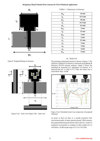
II. ANTENNA STRUCTURE
Proposed antenna is designed in three phases. In first phase a
rectangle patch with partial ground is designed as shown in
figure 1.In next phase a single step is created at lower edges
of patch of figure 1 to match antenna for UWB bandwidth as
given in figure 2 & in last phase a slotline of inverted hat type
is etched at centre of modified patch antenna of figure 2 and
design is given in figure 3 to make it a band rejected UWB
antenna. Dimensions of antennas are listed in table 1.
The antenna is fabricated on FR4 (roger) substrate
having thickness 1.65 mm & relative dielectric constant of
4.65. The area covered by antenna geometry is
.The antenna is simulated by Zeland’s
IE3D, MoM based simulator tool.
Figure1. Structure of Antenna
Designing of Band Notched Print Antenna for Ultra
Wideband Applications
Deepak Vyas, Suman Sankhla, Sunil Sharma](https://image.slidesharecdn.com/ijetr011101-171121162555/85/Ijetr011101-1-320.jpg)

![International Journal of Engineering and Technical Research (IJETR)
ISSN: 2321-0869, Volume-1, Issue-1, March 2013
5 www.erpublication.org
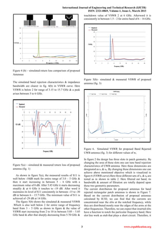
Figure 9 Simulated & Measured gain of proposed band
rejected UWB antenna (fig.2)
IV. CONCLUSION
. A novel compact band notched ultra wideband rectangle
printed antenna has been designed. The impedance
bandwidth is much higher than required UWB band which
can be used by future application of UWB systems. Moreover
by visualizing radiation pattern, the proposed antenna can be
effectively used for UWB applications.
REFERENCES
[1] Yi-Cheng Lin and Kuan-Jung Hung, “Compact Ultra wideband
Rectangular Aperture Antenna and Band-Notched Designs”, IEEE
Transactions Antennas and Propagation Vol. 54, No. 11, November 2006
[2] Tao Yuan, Cheng Wei Qiu, Le Wei Li,1Mook Seng Leong and Qun
Zhang, “Elliptically Shaped Ultra Wide Band Patch Antenna with Band –
Notch Features”, Microwave & Optical Technology Letters Vol. 50, No.
3, March 2008
[3] Wen-jun Lui, Chong-hu Cheng, and Hong-bo Zhu, “Improved Frequency
Notched Ultra wideband Slot Antenna Using Square Ring Resonator”.
IEEE Transactions Antennas and Propagation Vol. 55, No. 9, September
2007
[4] Qing Qi Pei, Cheng-Wei Qiu, Tao Yuan, and Said Zouhdi, “Hybrid
Shaped Ultra Wide Band Antenna”, Microwave and Optical Technology
Letters, Vol. 49, No. 10, October 2007
[5] X.C.Yin, C.L.Ruan, S.G.Mo, C.Y.Ding, and J.H.Chu, “A Compact Ultra
Wide Band Microstrip Antenna with multiple Notches”, PIER 84,
321–332, 2008
[6] S.H. Choi, J.K. Park, S.K. Kim and J.Y. Park, “A new ultra-wideband
antenna for UWB applications”, Microwave Opt. Technol. Lett., Vol. 40,
No. 5, pp. 399-401, Mar. 2004
[7] Jia Yi Sze and Jen Yi Shiu, “Design of Band-Notched Ultra wideband
Square aperture Antenna With a Hat-Shaped Back-Patch”, IEEE
Transactions Antennas and Propagation Vol. 56, No.10, October 2008](https://image.slidesharecdn.com/ijetr011101-171121162555/85/Ijetr011101-5-320.jpg)

This paper presents a new ultra wideband (UWB) antenna with a band notch feature designed to minimize interference with WLAN at frequencies between 5.15 GHz and 5.85 GHz. The antenna achieves a wide impedance bandwidth of 3.15 GHz to 15.7 GHz and employs a simple structure, utilizing three slots to create the band rejection characteristic. Results indicate the antenna maintains a return loss significantly below -10 dB across the intended bandwidth, confirming its suitability for UWB applications.