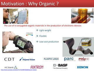
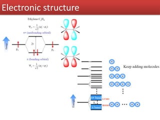
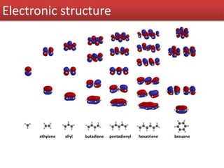
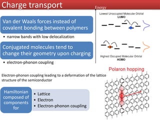
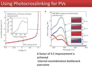
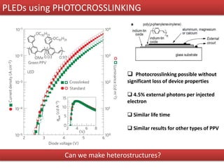
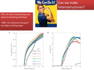
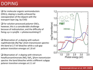
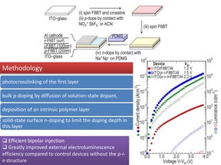
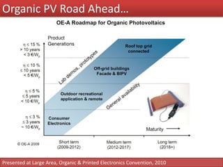
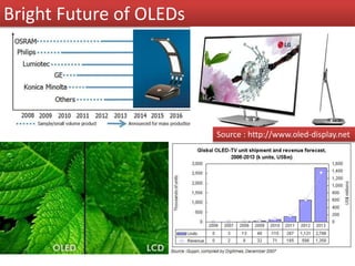
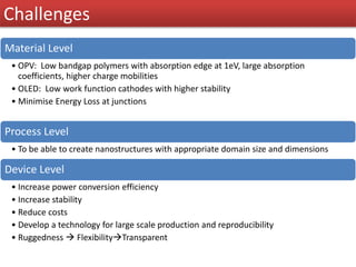
Plastic Organic Electronics
Presented by :
Dagmawi Belaineh
Shuvan Prashant Turaga
As part of PC5212 Physics of Nanostructures Coursework
Outline
Introduction Organic LEDs
Organic
Photovoltaics
State of the
art
Conclusion
The use of π-conjugated organic materials in the production of electronic devices
 Light weight
 Flexible
 Low-cost production
http://www.youtube.com/watch?v=TDuP8PtDJbE&feature=related
Motivation : Why Organic ?
X
Nobel Chemistry 2000 goes to
For their work on conductive polymers…
Electronic structure
ethylene allyl butadiene pentadienyl hexatriene benzene
Electronic structure
Van der Waals forces instead of
covalent bonding between polymers
• narrow bands with low delocalization
Conjugated molecules tend to
change their geometry upon charging
• electron-phonon coupling
Electron-phonon coupling leading to a deformation of the lattice
structure of the semiconductor
• Lattice
• Electron
• Electron-phonon coupling
Hamiltonian
composed of
components
for
Charge transport Energy
Sir Richard Friend
Tan Chin Tuan Centennial Professor
Polymer Light-Emitting Diodes
http://www.lti.unikarlsruhe.de/rd_download/polymer2004/Plastic_Electronic_WS0405_7.pdf
PLED BASICS
Heterostructures
Light emission process
rst is the fraction of singlet excitons,
q is the efficiency of radiative decay of these singlet excitons
Understanding Efficiency
circuitexternalin theflowingelectrons#
devicehewithin teventsformationexciton#

Organic Photovoltaics
Source : KonarkaC. W. Tang, Appl. Phys. Lett. 1985, 48, 183
Major Milestone :
Tang reported single
heterojunction device OPV
in 1985 with a power
efficiency of 1%
High optical absorption
coefficients of organic
molecules  thinner solar
cells
Photon
Absorption ~1fs
ηa
Exciton
Formation
~100fs to 1ns
Exciton Diffusion
~ 1ns
ηED
Exciton Breakup
~ 100 fs
Charge transport
ηCT
Charge
Collection ~1 us
ηCC
OPVs : Device Physics
A
N
O
D
E
C
A
T
H
O
D
E
-
+
LUMO
HOMO
Light
External Quantum Efficiency(EQE) = ηa ηED ηEB ηCT ηCC
DONOR ACCEPTOR
Characterization
IV Characteristics
η = maximum
deliverable
electrical
power(VM ×JM)
to the incident
light power(Pinc)
FF = Fill Factor
VOC = Open Circuit
Voltage
JSC= Short Circuit
Current
Materials,
• Printing
– Screen Printing
– Stamping
• Spraying
• Spin Coating
• Vaporization
Acceptors
PCPDTBT,
MEH-PPV,
P3HT, PTB1
Donors
PCDTBT,
PCBM,
PSBTBT
Electrode
Al, Ca, Ag
Transparent
Electrode
PEDOT:PSS,
ITO
Krebs F. C., Solar Energy Materials & Solar Cells 93 (2009) 394–412
Processes
Organic Solar Cell Architectures
Planar Heterojunction
Typically exciton diffusion length = 10 nm
 Layer width limited
But atleast should be 100 nm to absorb light
completely
Glass
Transparent Electrode
Donor Layer
Acceptor Layer
Metal Electrode Bulk Heterojunction
Ordered
Heterojunction
Now, actual Solar Cells can be complex…
Stacking improves efficiency
Adding more
layers for hole
injection and
electron
injection adds
to the cells
efficiency
Tandem Cell is better
Tandem Cell
Jsc = 7.8 mA/cm2, Voc = 1.24 V, FF =
0.67, and ηe = 6.5%
www.sciencemag.org SCIENCE VOL 317 13 JULY 2007 pp. 223-225
Progress in Solar Cell Research
5.4%
NREL Database
State of the art :
• Spin coating
– Can coat large areas with
high speed
– Redissolution
– Patterning not possible as
• Vapour Evaporation
– Layer by layer without
chemical interaction in
vacuum
– Non uniform, requires
UHV, expensive,
contamination, LOS
• Vapour Deposition
– Better control through gas
flow rate and temperature
– Uniformity and not
contaminated
State of the art : Photocrosslinking
Photolysis of FPA gives singlet nitrene
which inserts into C-H bonds of polymers
to form crosslinks
Effective crosslinker conc is low !!
FPA Methodology
Roll 2 Roll Manufacturing
DUV
Solvent
Wash
Spin Coating/ Ink Jet Printing
DUV
Solvent
Wash
Key Advantage : Continuity for e and h conduction paths is guaranteed.
Contiguous Interpenetrating Structure for PVs
Using Photocrosslinking for PVs
A factor of 4.5 improvement is
achieved
internal recombination bottleneck
overcome
 Photocrosslinking possible without
significant loss of device properties
 4.5% external photons per injected
electron
 Similar life time
 Similar results for other types of PPV
Can we make heterostructures?
PLEDs using PHOTOCROSSLINKING
ITO
TFB the hole-transporting and
electron-blocking interlayer
F8BT the electron-transport
and light-emitting layer
Can we make
heterostructures?
 For solution-processed polymer OSCs,
however, this is a considerable challenge
because of redissolution, and the difficulty of
fixing a p-i-n profile -> photocrosslinking!!!
 For molecular organic semiconductors
(OSCs), doping is readily achieved by
coevaporation of the dopant with the
transport layer (eg. by CVD)
 Observation of p-doping with sodium
naphthalenide (Na+Np−) from transmission spectra:
the band at 2.7 eV bleaches while a sub-gap
polaron transition emerges at 1.8 eV
 Observation of n-doping with nitronium
hexafluoroantimonate (NO2
+SbF6
−)from transmission
spectra: the band bleaches while a different subgap
polaron transition emerges at 2.1 eV
DOPING
Sivaramakrishnan et al, APL 2009
 Efficient bipolar injection
 Greatly improved external electroluminescence
efficiency compared to control devices without the p-i-
n structure
photocrosslinking of the first layer
bulk p-doping by diffusion of solution-state dopant,
deposition of an intrinsic polymer layer
solid-state surface n-doping to limit the doping depth in
this layer
Methodology
Organic PV Road Ahead…
Presented at Large Area, Organic & Printed Electronics Convention, 2010
Bright Future of OLEDs
Source : http://www.oled-display.net
Challenges
Material Level
• OPV: Low bandgap polymers with absorption edge at 1eV, large absorption
coefficients, higher charge mobilities
• OLED: Low work function cathodes with higher stability
• Minimise Energy Loss at junctions
Process Level
• To be able to create nanostructures with appropriate domain size and dimensions
Device Level
• Increase power conversion efficiency
• Increase stability
• Reduce costs
• Develop a technology for large scale production and reproducibility
• Ruggedness  FlexibilityTransparent
Summary
• Organic Electronics has tremendous potential of
replacing the present rigid electronics.
• However, there are issues of cost-efficiency tradeoff
which need to be dealt with.
• Competitive research among the companies is
empowering the progress of organics.
• Dynamic and highly interdisciplinary field:
physicists, chemist, material scientists, electrical
engineers … truly Nano!
Sources
1. http://parsleyspics.blogspot.com/2011/02/stop-glenn-beck-new-petition-letter.html
2. http://courses.chem.psu.edu/chem210/mol-gallery/pi-systems/pisystems.html
3. http://www.blazedisplay.com/LCD_Knowledge.asp?Id=48
4. J.H. van Lienden, Charge transport in trans-polyacetylene, Thesis, Rijksuniversiteit Groningen (2006)
5. K. Walzer, B. Maennig, M. Pfeiffer, and K. Leo, Highly Efficient Organic Devices Based on Electrically
Doped Transport
6. Layers, Chem. Rev. 107, 1233-1271 (2007)
7. M. Pfeiffer, S.R. Forrest, K. Leo, M.E. Thompson, Electrophloroscent p-i-n OLEDS for very high efficiency
flat-panel displays, Adv. Mat. , 14, 22, (2002)
8. www.wikipedia.org

Plastic Electronics

  • 1.
    Plastic Organic Electronics Presentedby : Dagmawi Belaineh Shuvan Prashant Turaga As part of PC5212 Physics of Nanostructures Coursework
  • 2.
  • 3.
    The use ofπ-conjugated organic materials in the production of electronic devices  Light weight  Flexible  Low-cost production http://www.youtube.com/watch?v=TDuP8PtDJbE&feature=related Motivation : Why Organic ?
  • 4.
    X Nobel Chemistry 2000goes to For their work on conductive polymers…
  • 5.
  • 6.
    ethylene allyl butadienepentadienyl hexatriene benzene Electronic structure
  • 7.
    Van der Waalsforces instead of covalent bonding between polymers • narrow bands with low delocalization Conjugated molecules tend to change their geometry upon charging • electron-phonon coupling Electron-phonon coupling leading to a deformation of the lattice structure of the semiconductor • Lattice • Electron • Electron-phonon coupling Hamiltonian composed of components for Charge transport Energy
  • 8.
    Sir Richard Friend TanChin Tuan Centennial Professor Polymer Light-Emitting Diodes
  • 9.
  • 10.
  • 11.
  • 12.
    rst is thefraction of singlet excitons, q is the efficiency of radiative decay of these singlet excitons Understanding Efficiency circuitexternalin theflowingelectrons# devicehewithin teventsformationexciton# 
  • 13.
    Organic Photovoltaics Source :KonarkaC. W. Tang, Appl. Phys. Lett. 1985, 48, 183 Major Milestone : Tang reported single heterojunction device OPV in 1985 with a power efficiency of 1% High optical absorption coefficients of organic molecules  thinner solar cells
  • 14.
    Photon Absorption ~1fs ηa Exciton Formation ~100fs to1ns Exciton Diffusion ~ 1ns ηED Exciton Breakup ~ 100 fs Charge transport ηCT Charge Collection ~1 us ηCC OPVs : Device Physics A N O D E C A T H O D E - + LUMO HOMO Light External Quantum Efficiency(EQE) = ηa ηED ηEB ηCT ηCC DONOR ACCEPTOR
  • 15.
    Characterization IV Characteristics η =maximum deliverable electrical power(VM ×JM) to the incident light power(Pinc) FF = Fill Factor VOC = Open Circuit Voltage JSC= Short Circuit Current
  • 16.
    Materials, • Printing – ScreenPrinting – Stamping • Spraying • Spin Coating • Vaporization Acceptors PCPDTBT, MEH-PPV, P3HT, PTB1 Donors PCDTBT, PCBM, PSBTBT Electrode Al, Ca, Ag Transparent Electrode PEDOT:PSS, ITO Krebs F. C., Solar Energy Materials & Solar Cells 93 (2009) 394–412 Processes
  • 17.
    Organic Solar CellArchitectures Planar Heterojunction Typically exciton diffusion length = 10 nm  Layer width limited But atleast should be 100 nm to absorb light completely Glass Transparent Electrode Donor Layer Acceptor Layer Metal Electrode Bulk Heterojunction Ordered Heterojunction
  • 18.
    Now, actual SolarCells can be complex… Stacking improves efficiency Adding more layers for hole injection and electron injection adds to the cells efficiency
  • 19.
    Tandem Cell isbetter Tandem Cell Jsc = 7.8 mA/cm2, Voc = 1.24 V, FF = 0.67, and ηe = 6.5% www.sciencemag.org SCIENCE VOL 317 13 JULY 2007 pp. 223-225
  • 20.
    Progress in SolarCell Research 5.4% NREL Database
  • 21.
    State of theart : • Spin coating – Can coat large areas with high speed – Redissolution – Patterning not possible as • Vapour Evaporation – Layer by layer without chemical interaction in vacuum – Non uniform, requires UHV, expensive, contamination, LOS • Vapour Deposition – Better control through gas flow rate and temperature – Uniformity and not contaminated
  • 22.
    State of theart : Photocrosslinking Photolysis of FPA gives singlet nitrene which inserts into C-H bonds of polymers to form crosslinks Effective crosslinker conc is low !!
  • 23.
    FPA Methodology Roll 2Roll Manufacturing DUV Solvent Wash Spin Coating/ Ink Jet Printing DUV Solvent Wash
  • 24.
    Key Advantage :Continuity for e and h conduction paths is guaranteed. Contiguous Interpenetrating Structure for PVs
  • 25.
    Using Photocrosslinking forPVs A factor of 4.5 improvement is achieved internal recombination bottleneck overcome
  • 26.
     Photocrosslinking possiblewithout significant loss of device properties  4.5% external photons per injected electron  Similar life time  Similar results for other types of PPV Can we make heterostructures? PLEDs using PHOTOCROSSLINKING
  • 27.
    ITO TFB the hole-transportingand electron-blocking interlayer F8BT the electron-transport and light-emitting layer Can we make heterostructures?
  • 28.
     For solution-processedpolymer OSCs, however, this is a considerable challenge because of redissolution, and the difficulty of fixing a p-i-n profile -> photocrosslinking!!!  For molecular organic semiconductors (OSCs), doping is readily achieved by coevaporation of the dopant with the transport layer (eg. by CVD)  Observation of p-doping with sodium naphthalenide (Na+Np−) from transmission spectra: the band at 2.7 eV bleaches while a sub-gap polaron transition emerges at 1.8 eV  Observation of n-doping with nitronium hexafluoroantimonate (NO2 +SbF6 −)from transmission spectra: the band bleaches while a different subgap polaron transition emerges at 2.1 eV DOPING Sivaramakrishnan et al, APL 2009
  • 29.
     Efficient bipolarinjection  Greatly improved external electroluminescence efficiency compared to control devices without the p-i- n structure photocrosslinking of the first layer bulk p-doping by diffusion of solution-state dopant, deposition of an intrinsic polymer layer solid-state surface n-doping to limit the doping depth in this layer Methodology
  • 30.
    Organic PV RoadAhead… Presented at Large Area, Organic & Printed Electronics Convention, 2010
  • 31.
    Bright Future ofOLEDs Source : http://www.oled-display.net
  • 32.
    Challenges Material Level • OPV:Low bandgap polymers with absorption edge at 1eV, large absorption coefficients, higher charge mobilities • OLED: Low work function cathodes with higher stability • Minimise Energy Loss at junctions Process Level • To be able to create nanostructures with appropriate domain size and dimensions Device Level • Increase power conversion efficiency • Increase stability • Reduce costs • Develop a technology for large scale production and reproducibility • Ruggedness  FlexibilityTransparent
  • 33.
    Summary • Organic Electronicshas tremendous potential of replacing the present rigid electronics. • However, there are issues of cost-efficiency tradeoff which need to be dealt with. • Competitive research among the companies is empowering the progress of organics. • Dynamic and highly interdisciplinary field: physicists, chemist, material scientists, electrical engineers … truly Nano!
  • 34.
    Sources 1. http://parsleyspics.blogspot.com/2011/02/stop-glenn-beck-new-petition-letter.html 2. http://courses.chem.psu.edu/chem210/mol-gallery/pi-systems/pisystems.html 3.http://www.blazedisplay.com/LCD_Knowledge.asp?Id=48 4. J.H. van Lienden, Charge transport in trans-polyacetylene, Thesis, Rijksuniversiteit Groningen (2006) 5. K. Walzer, B. Maennig, M. Pfeiffer, and K. Leo, Highly Efficient Organic Devices Based on Electrically Doped Transport 6. Layers, Chem. Rev. 107, 1233-1271 (2007) 7. M. Pfeiffer, S.R. Forrest, K. Leo, M.E. Thompson, Electrophloroscent p-i-n OLEDS for very high efficiency flat-panel displays, Adv. Mat. , 14, 22, (2002) 8. www.wikipedia.org