SEMINAR BY: RAHUL RAGHVENDRA
USN- 1MV11 EC076
 WHAT IS MoS2?
 WHY MoS2?
 PROPERTIES OF MoS2
 ENERGY BAND STRUCTURE
 ENERGY BAND ENGINEERING
 CARRIER MOBILITY
 FABRICATION METHODS
 DEVICE APPLICATIONS
 CONCLUSIONS and OUTLOOK
Since the invention of the first transistor, silicon has been at the
heart of electronics but as the demands increases , we are asking way
too much out of silicon thus for all its drawbacks scientists began
searching for futuristic elements that can replace and even
outperform silicon.
This search led us to MoS2- single layer and few monolayer thick
2-dimensional semiconductor.
Its unique physical properties outperforms silicon and its closest
competitor graphene.
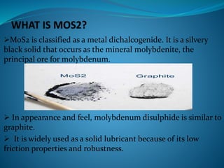
MoS2 is classified as a metal dichalcogenide. It is a silvery
black solid that occurs as the mineral molybdenite, the
principal ore for molybdenum.
 In appearance and feel, molybdenum disulphide is similar to
graphite.
 It is widely used as a solid lubricant because of its low
friction properties and robustness.
Excellent gate control
Saturation
Scalability
High current capability
Very low noise
Wide direct band gap
It exhibits good electrical and transport properties
Chemically and thermally stable
Transparent and flexible
Relatively inexpensive
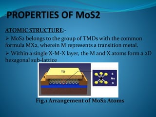
ATOMIC STRUCTURE:-
 MoS2 belongs to the group of TMDs with the common
formula MX2, wherein M represents a transition metal.
 Within a single X-M-X layer, the M and X atoms form a 2D
hexagonal sub-lattice
Fig.1 Arrangement of MoS2 Atoms
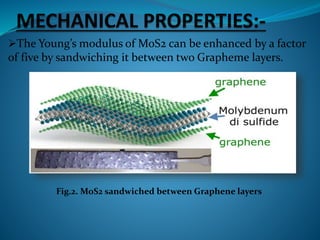
The Young’s modulus of MoS2 can be enhanced by a factor
of five by sandwiching it between two Grapheme layers.
Fig.2. MoS2 sandwiched between Graphene layers
MoS2 also has the advantage that it is as stiff as stainless steel
but is also capable of being flexible.
It can be bent to large angles and can be stretched upto 10% of
its length.
It has a key advantage over graphene- it can amplify electronic
signals at room temperature, while graphene must be cooled to
70 Kelvin- cold enough for nitrogen to turn into liquid.
 Along with the other group-VI layered compounds, MoS2
exhibits semiconducting behavior.
The fundamental indirect band gap of bulk MoS2 is 1.22 to
1.23 eV, while the direct band gap ranges from 1.74 to 1.77 eV.
In 1973 Mattheiss used a non relativistic augmented-plane-
wave (APW) method to calculate the electronic band
structures of several TMDs, including MoS2.
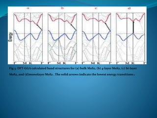
Fig 3. DFT-GGA calculated band structures for (a) bulk MoS2, (b) 4-layer MoS2, (c) bi-layer
MoS2, and (d)monolayer MoS2 . The solid arrows indicate the lowest energy transitions.
MECHANICAL STRAIN:-
 Mechanical strain can strongly affect the band structure,
carrier effective masses, and transport, optical, and magnetic
properties of MoS2 via changing the distance between the
atoms and also the crystal symmetry.
 Larger strain can be applied to low-dimensional MoS2 due
to its mechanical flexibility, and its properties can be tuned
by applied strain, which opens possibilities for developing
new tunable electronic devices.
 The energy band gap gradually decreases with increasing
tensile strain, whereas it initially rises and then decreases
linearly under applied compressive strain.
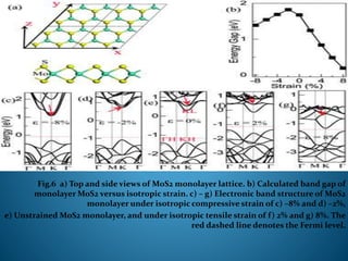
Fig.6 a) Top and side views of MoS2 monolayer lattice. b) Calculated band gap of
monolayer MoS2 versus isotropic strain. c) – g) Electronic band structure of MoS2
monolayer under isotropic compressive strain of c) –8% and d) –2%,
e) Unstrained MoS2 monolayer, and under isotropic tensile strain of f) 2% and g) 8%. The
red dashed line denotes the Fermi level.
 The hole mobility (96.62 cm2 V−1 s−1) in monolayer sheets
of MoS2 is about twice that of the electron mobility (43.96
cm2 V−1 s−1).
 The highest mobility value of 700 cm2 V−1 s−1 was
reported for a back-gated FET based on 10-nm-thick
multilayer MoS2 flake.
 The charge mobilities in MoS2 armchair nanoribbons can
be regulated by edge modification owing to the changing
electronic structures. In pristine armchair nanoribbons, the
electron and hole mobilities are about 30 cm2 V−1 s−1 and 25
cm2 V−1 s−1, respectively.
[1]. MECHANICAL EXFOLIATION TECHNIQUE:-
Single and multilayer MoS2 films are deposited onto
Si/SiO2 using the mechanical exfoliation technique.
 The films were then used for the fabrication of field-
effect transistors.
 These FET devices can be used as gas sensors to
detect nitrous oxide (NO).
 Selective solution method to prepare Molybdenum
Disulfide (MoS2) thin films for functional thin film
transistors (TFTs).
 The selective area solution-processed MoS2grows on top
and around the gold (Au) source and drain electrodes and
in the channel area of the TFT. MoS2 thicknesses in the
channel area are in the order of 11 nm
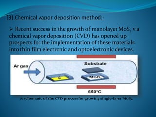
 Recent success in the growth of monolayer MoS2 via
chemical vapor deposition (CVD) has opened up
prospects for the implementation of these materials
into thin film electronic and optoelectronic devices.
A schematic of the CVD process for growing single-layer MoS2
MoS2 has a wide range of applications.
 This material is highly anisotropic with excellent
nonlinear optical properties and also is a very good
lubricant.
 The layered material helps the membranes to have
mechanical strengths some 30 times higher than that of
steel.
 It has stability at up to 1100 ◦C in an inert atmosphere.
 It has a key advantage over graphene- it can amplify
electronic signals at room temperature whereas graphene
must be cooled at 70 kelvin.
 the mechanical strength and flexibility of these
materials, we demonstrate integration onto a polymer
substrate to create flexible and transparent FETs that
show unchanged performance up to 1.5% strain.
 Two-dimensional MoS2 may be used in sensors and
memory and photovoltaic devices. Direct band gap and
confinement effects in single-layer MoS2 makes this
material attractive for optoelectronics.
 Ultrasensitive monolayer-MoS2 phototransistors with
improved device mobility and ON currents have been
already demonstrated.
 Molybdenite (MoS2) has a number of benefits over
silicon (Si) when it comes to creating a micro chip. Future
chips using MoS2 will be smaller than silicon chips.
Reduced electricity consumption is another benefit, along
with mechanical flexibility.
 Two-dimensional materials, particularly the TMD mono
layers, are emerging as a new class of materials.
Among them, semiconducting MoS2 is gaining increasing
attention owing to an attractive combination of physical
properties, which include band gap tunability and
reasonably high electron mobility.
 On the experimental front, researchers have focused on s
practical applications of 2D MoS2, in particular the
development of field-effect transistors,and negligible off
current.
 Ultrasensitive phototransistors, logic circuits, and
amplifiers based on monolayer MoS2 have also been
demonstrated, with good output current saturation and
high currents.
 The flexibility, stretchability, and optical transparency of
monolayer MoS2 make it particularly attractive for
transparent and flexible electronics.
 Since the properties of MoS2 depend strongly on the
number of monolayers, techniques providing control over
the number of deposited monolayers are highly desirable.
 For use in flexible electronics, the major challenge is to
find approaches that would produce electronic-quality
material at deposition temperatures below 400 ◦C
necessitated by the need for growth directly on transparent
plastic substrates.
 Development of 2D MoS2-based devices, in particular
FETs, for real applications also requires further studies of
electrode and gate dielectric materials.
MoS2

MoS2

  • 1.
    SEMINAR BY: RAHULRAGHVENDRA USN- 1MV11 EC076
  • 2.
     WHAT ISMoS2?  WHY MoS2?  PROPERTIES OF MoS2  ENERGY BAND STRUCTURE  ENERGY BAND ENGINEERING  CARRIER MOBILITY  FABRICATION METHODS  DEVICE APPLICATIONS  CONCLUSIONS and OUTLOOK
  • 3.
    Since the inventionof the first transistor, silicon has been at the heart of electronics but as the demands increases , we are asking way too much out of silicon thus for all its drawbacks scientists began searching for futuristic elements that can replace and even outperform silicon. This search led us to MoS2- single layer and few monolayer thick 2-dimensional semiconductor. Its unique physical properties outperforms silicon and its closest competitor graphene.
  • 4.
    MoS2 is classifiedas a metal dichalcogenide. It is a silvery black solid that occurs as the mineral molybdenite, the principal ore for molybdenum.  In appearance and feel, molybdenum disulphide is similar to graphite.  It is widely used as a solid lubricant because of its low friction properties and robustness.
  • 5.
    Excellent gate control Saturation Scalability Highcurrent capability Very low noise Wide direct band gap It exhibits good electrical and transport properties Chemically and thermally stable Transparent and flexible Relatively inexpensive
  • 6.
    ATOMIC STRUCTURE:-  MoS2belongs to the group of TMDs with the common formula MX2, wherein M represents a transition metal.  Within a single X-M-X layer, the M and X atoms form a 2D hexagonal sub-lattice Fig.1 Arrangement of MoS2 Atoms
  • 7.
    The Young’s modulusof MoS2 can be enhanced by a factor of five by sandwiching it between two Grapheme layers. Fig.2. MoS2 sandwiched between Graphene layers
  • 8.
    MoS2 also hasthe advantage that it is as stiff as stainless steel but is also capable of being flexible. It can be bent to large angles and can be stretched upto 10% of its length. It has a key advantage over graphene- it can amplify electronic signals at room temperature, while graphene must be cooled to 70 Kelvin- cold enough for nitrogen to turn into liquid.
  • 9.
     Along withthe other group-VI layered compounds, MoS2 exhibits semiconducting behavior. The fundamental indirect band gap of bulk MoS2 is 1.22 to 1.23 eV, while the direct band gap ranges from 1.74 to 1.77 eV. In 1973 Mattheiss used a non relativistic augmented-plane- wave (APW) method to calculate the electronic band structures of several TMDs, including MoS2.
  • 10.
    Fig 3. DFT-GGAcalculated band structures for (a) bulk MoS2, (b) 4-layer MoS2, (c) bi-layer MoS2, and (d)monolayer MoS2 . The solid arrows indicate the lowest energy transitions.
  • 11.
    MECHANICAL STRAIN:-  Mechanicalstrain can strongly affect the band structure, carrier effective masses, and transport, optical, and magnetic properties of MoS2 via changing the distance between the atoms and also the crystal symmetry.  Larger strain can be applied to low-dimensional MoS2 due to its mechanical flexibility, and its properties can be tuned by applied strain, which opens possibilities for developing new tunable electronic devices.  The energy band gap gradually decreases with increasing tensile strain, whereas it initially rises and then decreases linearly under applied compressive strain.
  • 12.
    Fig.6 a) Topand side views of MoS2 monolayer lattice. b) Calculated band gap of monolayer MoS2 versus isotropic strain. c) – g) Electronic band structure of MoS2 monolayer under isotropic compressive strain of c) –8% and d) –2%, e) Unstrained MoS2 monolayer, and under isotropic tensile strain of f) 2% and g) 8%. The red dashed line denotes the Fermi level.
  • 13.
     The holemobility (96.62 cm2 V−1 s−1) in monolayer sheets of MoS2 is about twice that of the electron mobility (43.96 cm2 V−1 s−1).  The highest mobility value of 700 cm2 V−1 s−1 was reported for a back-gated FET based on 10-nm-thick multilayer MoS2 flake.  The charge mobilities in MoS2 armchair nanoribbons can be regulated by edge modification owing to the changing electronic structures. In pristine armchair nanoribbons, the electron and hole mobilities are about 30 cm2 V−1 s−1 and 25 cm2 V−1 s−1, respectively.
  • 14.
    [1]. MECHANICAL EXFOLIATIONTECHNIQUE:- Single and multilayer MoS2 films are deposited onto Si/SiO2 using the mechanical exfoliation technique.  The films were then used for the fabrication of field- effect transistors.  These FET devices can be used as gas sensors to detect nitrous oxide (NO).
  • 15.
     Selective solutionmethod to prepare Molybdenum Disulfide (MoS2) thin films for functional thin film transistors (TFTs).  The selective area solution-processed MoS2grows on top and around the gold (Au) source and drain electrodes and in the channel area of the TFT. MoS2 thicknesses in the channel area are in the order of 11 nm
  • 16.
     Recent successin the growth of monolayer MoS2 via chemical vapor deposition (CVD) has opened up prospects for the implementation of these materials into thin film electronic and optoelectronic devices. A schematic of the CVD process for growing single-layer MoS2
  • 17.
    MoS2 has awide range of applications.  This material is highly anisotropic with excellent nonlinear optical properties and also is a very good lubricant.  The layered material helps the membranes to have mechanical strengths some 30 times higher than that of steel.  It has stability at up to 1100 ◦C in an inert atmosphere.  It has a key advantage over graphene- it can amplify electronic signals at room temperature whereas graphene must be cooled at 70 kelvin.
  • 18.
     the mechanicalstrength and flexibility of these materials, we demonstrate integration onto a polymer substrate to create flexible and transparent FETs that show unchanged performance up to 1.5% strain.
  • 19.
     Two-dimensional MoS2may be used in sensors and memory and photovoltaic devices. Direct band gap and confinement effects in single-layer MoS2 makes this material attractive for optoelectronics.  Ultrasensitive monolayer-MoS2 phototransistors with improved device mobility and ON currents have been already demonstrated.  Molybdenite (MoS2) has a number of benefits over silicon (Si) when it comes to creating a micro chip. Future chips using MoS2 will be smaller than silicon chips. Reduced electricity consumption is another benefit, along with mechanical flexibility.
  • 20.
     Two-dimensional materials,particularly the TMD mono layers, are emerging as a new class of materials. Among them, semiconducting MoS2 is gaining increasing attention owing to an attractive combination of physical properties, which include band gap tunability and reasonably high electron mobility.  On the experimental front, researchers have focused on s practical applications of 2D MoS2, in particular the development of field-effect transistors,and negligible off current.
  • 21.
     Ultrasensitive phototransistors,logic circuits, and amplifiers based on monolayer MoS2 have also been demonstrated, with good output current saturation and high currents.  The flexibility, stretchability, and optical transparency of monolayer MoS2 make it particularly attractive for transparent and flexible electronics.  Since the properties of MoS2 depend strongly on the number of monolayers, techniques providing control over the number of deposited monolayers are highly desirable.
  • 22.
     For usein flexible electronics, the major challenge is to find approaches that would produce electronic-quality material at deposition temperatures below 400 ◦C necessitated by the need for growth directly on transparent plastic substrates.  Development of 2D MoS2-based devices, in particular FETs, for real applications also requires further studies of electrode and gate dielectric materials.