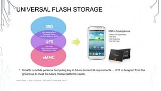
Universal Flash Storage is an upcoming memory specification for use in mobile phones, tablets and other consumer electronics devices.
It is the successor of Embedded Multimedia controller (eMMC) that currently prevails and will be available as storage in on-chip and expandable form (in the form of memory cards).
2. HISTORY OF MASS STORAGE
UNIVERSAL FLASH STORAGE - ECEN5613 - BHAUMIK BHATT
• Memory storage market has been flooded with a plethora of different types of cards for
different portable devices. So far, as we have seen, Secure Digital (SD) card specification
by SanDisk has been tremendously popular and has gained wide-spread adoption.
• However, there are different cards that still exist. Examples: Compact Flash (CF) cards and
XD picture cards for digital cameras, and so on.
3. UNIVERSAL FLASH STORAGE
• JEDEC stands for Joint Electron Device Engineering Council. It is now known as JEDEC Solid State
Technology Association. JESD220A v1.0 made released in 2011. JESD220A v1.1 released in June 2012.
JESD220B v2.0 announced September 2013.
• Being a common flash specification, UFS specification aims to is to bring high data rates, increased
reliability and a subsequent reduction in market confusion with a plethora of existing flash cards.
• The proposed specification is backed by leading firms such as Nokia, Sony Ericsson, Texas Instruments,
STMicroelectronics, Samsung and Micron.
• Toshiba was the first to announce 64 GB UFS Nand (v1.1) embedded storage to enable chipset and OS
vendors to develop the interface for the emerging standard. Mass production, as stated by Toshiba,
begins Q2 of 2014 for V 2.0.
• UFS supports both removable cards and embedded packages.
• UFS is NOT backwards compatible to the eMMC.
UNIVERSAL FLASH STORAGE - ECEN5613 - BHAUMIK BHATT
4. UNIVERSAL FLASH STORAGE
• Growth in mobile personal computing key to future demand & requirements… UFS is designed from the
ground-up to meet the future mobile platforms needs.
UNIVERSAL FLASH STORAGE - ECEN5613 - BHAUMIK BHATT
5. ADVANTAGES IN COMPARISON TO EMMC
• High speed serial interface compared to eMMC, which is a parallel interface.
• Ease of integration into embedded applications.
• Full duplex read/write operations.
• Uses the SCSI architectural model, unlike eMMC.
• Overall low power consumption, due to faster read/write operations and more idle time.
UNIVERSAL FLASH STORAGE - ECEN5613 - BHAUMIK BHATT
9. ELECTRICAL INTERFACE (PHYSICAL
LAYER)
• UniProSM (or Unified Protocol) is a high-
speed interface technology for
interconnecting integrated circuits in
portable devices, with support for UFS.
• UFS uses the MIPI M-PHY electrical
interface, supported by Versions 1.4 and
beyond of UniPro physical layer.
• UFS uses MIPI M-PHY as the physical layer
and MIPI UniPro as the link layer.
• With SCSI architecture model,
asynchronous operation and command
queuing for increased random read/write
speeds can be leveraged.
UniPro interconnection schematic
UNIVERSAL FLASH STORAGE - ECEN5613 - BHAUMIK BHATT
10. UFS V1.1 TEST-BED (TOSHIBA)
• Toshiba's comprehensive UFS 'ecosystem' brings together a UFS memory
device, UFS host controller IP and UFS software drivers.
UNIVERSAL FLASH STORAGE - ECEN5613 - BHAUMIK BHATT
11. CONCEPTUAL BLOCK DIAGRAM
• UIC is the lowest layer of UFS layered architecture. It handles
connection between UFS host and UFS device.
• UTP transports messages through UFS protocol information
unit(UPIU).
• Application layer handles SCSI commands supported by the UFS
specification.
UNIVERSAL FLASH STORAGE - ECEN5613 - BHAUMIK BHATT
12. COMMAND FLOW
• HCI processes 3 types of
commands in the following
priority
• Interconnect layer commands
• Transfer request
• Transfer management request
• These are transferred in the
form of a UFS Protocol
Information Unit between Host
and device.UNIVERSAL FLASH STORAGE - ECEN5613 - BHAUMIK BHATT
14. COMMAND QUEUING MECHANISM
• The UFS standard adopts the
well-known SCSI Architecture
Model and command protocols
supporting multiple commands
with command queuing features
and enabling a multi-thread
programming paradigm.
• The UFS HCI specification and
the adoption of SCSI provide a
well-known software programming
model and are enabling wider
market adoption.
UNIVERSAL FLASH STORAGE - ECEN5613 - BHAUMIK BHATT
15. SUPPORT FOR EMBEDDED AND
REMOVABLE MEDIA AND POSSIBLE
CHALLENGES
• Reduced IP licensing and hardware cost by sharing same protocol and same port (PHY)
• Problem: Latency increase for memories located further down the chain.
• Ways to deal with it?
• Lightly use communication links to avoid contention in the upstream and downstream
bus.
• Host controller needs to send as many read/write requests to memories for maximum
Bandwidth.
UNIVERSAL FLASH STORAGE - ECEN5613 - BHAUMIK BHATT
16. ADOPTION
• The e-MMC market size and momentum will likely mean that these two
mobile embedded solutions will continue to be supported in parallel for some
time, with UFS initially supporting the needs of applications demanding
higher performance, and typically at higher densities, and e-MMC supporting
the needs of applications driven to maintain the lowest cost.
• Qualcomm Snapdragon 805 with UFS support in works.
• The Universal Flash Storage Association (UFSA) was founded in 2010 as an
open Trade Association to promote widespread industry adoption and
acceptance of the UFS standard.
UNIVERSAL FLASH STORAGE - ECEN5613 - BHAUMIK BHATT
Memory storage market has been flooded with a plethora of different types of cards for different portable devices. So far, as we have seen, Secure Digital (SD) card specification by SanDisk has been tremendously popular and has gained wide-spread adoption.However, there are different cards that still exist. Examples: Compact Flash (CF) cards and XD picture cards for digital cameras, and so on.NAND - raw flash memoryRaw flash uses its own protocol, and this protocol includes reading pages, writing pages, and erasing blocks. It does not work like disks - disks are able to read blocks and write blocks, flash is able to read and write pages - and a set of pages called a block must be erased before you can write new data. You can only erase a limited number of times before the block wears out and won't fully erase anymore.SD - "Secure Digital"It's a memory card format. SD cards contain a tiny microcontroller and NAND. The microcontroller implements a FTL (Flash Translation Layer) that takes disk-like block accesses and translates it into meaningful NAND operations, as well as performing wear-leveling and block sparing. SD cards use the SPI protocol on the "host" side. USB SD card readers convert from USB mass storage commands to SPI SD commands.eMMC - embedded MMCThis refers to basically what you can think of as an SD card that's built into a motherboard (SD and MMC standards are very similar - enough that SD card readers can typically read MMC cards) - typically soldered in and non-removeable. Typically it is connected to the rest of the hardware via an internal SPI bus. Cell phones and ARM hardware, and other embedded-type devices (i.e. routers) may have this.SSD - "Solid State Drive"A controller + a bunch of NAND placed into a hard drive case. The controller implements a FTL (Flash Translation Layer) that takes disk-like block accesses and translates it into meaningful NAND operations, as well as performing wear-leveling and block sparing. Some controller types like "Sandforce", etc. are well known. SSDs use the SATA protocol and connector on the "host" side.Flash Memory is the predominant storage medium in consumer electronics today, offering a wide range of non-volatile memory solutions having high density, low power usage and endurance characteristics. Flash offers low cost, high performance, and reliable storage solutions for products ranging from smartphones to portable GPS units, gaming systems, digital cameras and portable computing devices.As applications for flash have become more diverse, the need for industry standard solutions has grown.
Ref: WikipediaToshiba was the first to announce 64 GB UFS Nand (v1.1) embedded storage to enable chipset and OS vendors to develop the interface for the emerging standard.Mass production, as stated by Toshiba, begins Q2 of 2014 for V 2.0.UFS supports both removable cards and embedded packages.
Growth in mobile personal computing key to future demand & requirements… UFS is designed from the ground-up to meet the future mobile platforms needs.Ref: Samsung.
MIPI Mobile Industry Processor InterfaceSCSI Small Computer System Interfacehttp://vimeo.com/72052801eMMC has a limitation to improve speed as data rates increase, precise timing among parallel I/O becomes more difficult. UFS has performance scalability (3Gbps -> 6Gbps…)Full duplex read/write operations support, unlike eMMC, which has half-duplex on a single bus.UFS supports command queuing, a method currently employed in SSDs, wherein the host system can send series of both read/write operations to the UFS. Maybe like how the CPU behaves during DMA?
http://www.toshiba.com/taec/Catalog/Line.do?familyid=7&subfamilyid=900116&lineid=2095185In UFS v2.0, the link bandwidth has been increased from 300 MB/s in UFS v1.1 to up to 600 MB/s per lane, and multilane support has been introduced allowing up to 1.2 GB/s per each data transfer direction.
The objective of UFSHCI is to provide a uniform interface method of accessing the UFS hardware capabilities so that a standard/common Driver can be provided for the Host Controller. ---
UFS BackgroundFirst published in February 2011, UFS is designed to be the most advanced specification for both embedded and removable Flash memory-based storage in mobile devices such as smartphones and tablets. The initial data throughput for UFS is 300 megabytes per second (MB/s) over the bus in both uplink and downlink directions simultaneously, without infringing on bandwidth needed for other applications. UFS offers a low active power level and a near-zero idle power level, which, combined with the power-saving attributes of the related MIPI specifications, allows for significant reductions in device power consumption. The UFS standard adopts the well-known SCSI Architecture Model and command protocols supporting multiple commands with command queuing features and enabling a multi-thread programming paradigm. This differs from conventional Flash-based memory cards and embedded Flash solutions which process one command at a time, limiting random read/write access performance. The UFS HCI specification and the adoption of SCSI provide a well-known software programming model and are enabling wider market adoption. D-PHYVersions 1.0 and 1.1 of UniPro use MIPI's D-PHY technology for the off-chip Physical Layer. This PHY allows inter-chip communication. Data rates of the D-PHY are variable, but are in the range of 500-1000 Mbit/s (lower speeds are supported, but at decreased power efficiency). The D-PHY was named after the Roman number for 500 ("D").The D-PHY uses differential signaling to convey PHY symbols over micro-stripline wiring. A second differential signal pair is used to transmit the associated clock signal from the source to the destination. The D-PHY technology thus uses a total of 2 clock wires per direction plus 2 signal wires per lane and per direction. For example a D-PHY might use 2 wires for the clock and 4 wires (2 lanes) for the data in the forward direction, but 2 wires for the clock and 6 wires (3 lanes) for the data in the reverse direction. Data traffic in the forward and reverse directions are totally independent at this level of the protocol stack.In UniPro, the D-PHY is used in a mode (called "8b9b" encoding) which conveys 8-bit bytes as 9-bit symbols. The UniPro protocol uses this to represent special control symbols (outside the usual 0 to 255 values). The PHY itself uses this to represent certain special symbols that have meaning to the PHY itself (e.g. IDLE symbols). Note that the ratio 8:9 can cause some confusion when specifying the data rate of the D-PHY: a PHY implementation running with a 450 MHz clock frequency is often rated as a 900 Mbit/s PHY, while only 800 Mbit/s is then available for the UniPro stack.The D-PHY also supports a Low-Power Data Transmission (LPDT) mode and various other low-power modes for use when no data needs to be sent.Versions 1.4 and beyond of UniPro support both the D-PHY as well as M-PHY[4] technology. The M-PHY technology is still in draft status, but supports high-speed data rates starting at about 1000 Mbit/s (the M-PHY was named after the Roman number for 1000). In addition to higher speeds, the M-PHY will use fewer signal wires because the clock signal is embedded with the data through the use of industry-standard 8b10b encoding. Again, a PHY capable of transmitting user data at 1000 Mbit/s is typically specified as being in 1250 Mbit/s mode due to the 8b10b encoding.Physical layer technologies supported by UniProPHY technology Version / Released Symbol encoding Mbit/s (payload) Signal wires Supported inD-PHY 1.00.00 / 14-May-2009 8b/9b up to circa 900 4 per direction UniPro 0.80 and upM-PHY 1.00.00 / Under adoption process 8b/10b 1000 and higher 2 per direction UniPro 1.40 and upThe D- and M-PHY are expected to co-exist for several years because the D-PHY is a less complex technology while the M-PHY provides higher bandwidths with fewer signal wires.Low speed modes and power savings[edit]It is worth noting that UniPro supports the power efficient low speed communication modes provided by both the D-PHY (10 Mbit/s) and M-PHY (3 Mbit/sec up to 500 Mbit/s). In these modes, power consumption roughly scales with the amount of data that is sent. Furthermore both PHY technologies provide additional power saving modes because they were optimized for use in battery-powered devices.---To achieve the highest performance and most power efficient data transport, JEDEC UFS aligns with industry–leading specifications from the MIPI® Alliance to form its Interconnect Layer. This collaboration continues with UFS v2.0, which supports the M-PHY® Version 3.0 specification and the UniProSM Version 1.6 specification.The MIPI® Alliance (MIPI) is an open membership organization that develops interface specifications for mobile and mobile-influenced industries. In July 2012 UniPro v1.40 has been upgraded to UniPro v1.41[6] to support the newer higher speed M-PHY v2.0.[7] The UniPro v1.4x specifications have been released together with a formal specification model (SDL)
UFS Protocol Information Unit: Information transfer (communication) between a UFS host and device is done through messages which are called UFS Protocol Information Units. UTP Transfer Request Descriptor: A data structure in system memory that contains a UTP command and additional contextual information needed to carry out the command operation. UTP Task Management Request Descriptor: A data structure in system memory that contains a UTP Task Management Function and the additional contextual information needed to execute the function. The UFS Host Controller is responsible for managing the interface between host SW and UFS device and the data transfer. This includes interface management, power management, and control. Also included in this standard is the data transfer & programming model.
Balancing these two conflicting goals is a key problem for UFS and requires developing a scheduling policy for slave and host controller that maximizes BW at minimum possible latency.
Current trends indicate JEDEC UFS has made it first to market leaving its other counterparts MIPI CSI3 and MIPI DSI2 behind in the race to harness the advantages of MIPI UniPro and MIPI M-PHY.At Arrow Devices, recently a casual lunch conversation turned in to intense debate on the reasons behind early adoption of JEDEC UFS over the MIPI CSI3 and MIPI DSI2. We compared these three technologies, as all three are end applications that will make use of MIPI UniPro and MIPI M-PHY as its service delivery mechanism.So what led to the faster adoption of JEDEC UFS over MIPI CSI3 and MIPI DSI2?Here is what we think on why this has happened…In a nutshell, it was driven by the broader and higher end user impact of JEDEC UFS as compared to MIPI CSI3 and MIPI DSI2.1. Greater end user impact: As mobile storage, JEDEC UFS has higher end user impact as it enhances user experience due to the following: Higher performance, efficiency & responsiveness - Leading to Instant ON, Multi-Tasking, Fast app loading and swapping Low Power – Longer Battery life even with larger screens and multi-taskingSecurity and Reliability – Enterprise application support and Secure Mobile shoppingSmall and Scalable – Thinner and lighter devices2. Easier technological integration: Along with end user impact, what seems to have enabled quicker adoption is ease of technology development and integration into products due to the following:Software compatibility with the wide spread SCSI framework - UFS 2.0 Specification follows the SCSI programming model enabling software reuseSimpler Host design due to the well-defined UFS Host controller interface (UFSHCI) specificationApart from these UFS 2.0 requires only single UniPro Transport layer CPort and does not use the built in end-to-end flow control capabilities of UniPro. It does not require the low latency TC1 support or Pre-emption. This leads to simplification of the MIPI UniPro controller design as well. 3. Better utilization of bandwidth: While MIPI CSI3 and DSI2 utilize significant one-way bandwidth, JEDEC UFS is able to fully utilize the duplex bandwidth provided by the MIPI UniPro transport. Authors: Neha Mittal and AnandShirahattihttp://www.arrowdevices.com/blog/how-did-jedec-ufs-beat-the-mipi-csi3-and-dsi2-in-adoption-race/