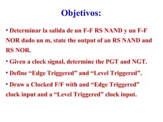
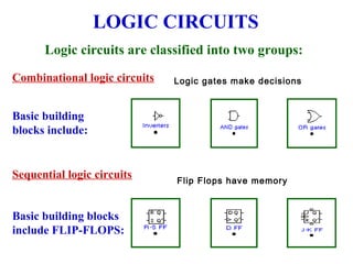
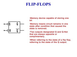
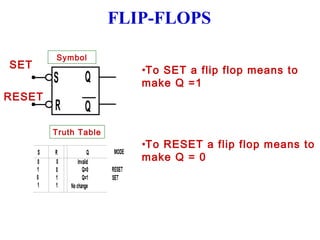
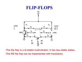
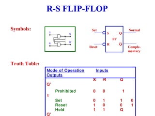
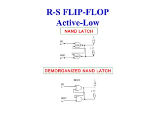
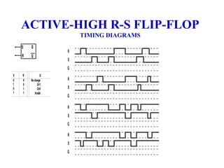
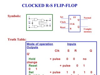
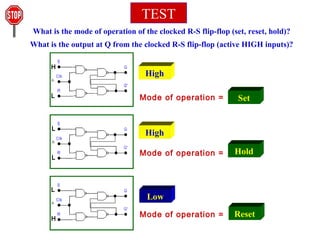
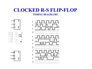
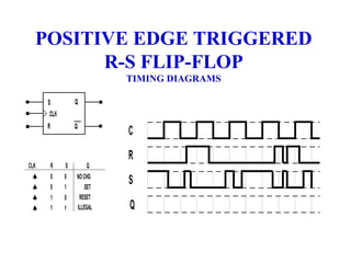
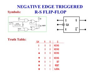
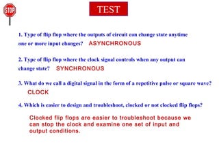
SlideShare a Scribd company logo
Electrónica Digital


       Flip-Flops
Objetivos:
• Determinar la salida de un F-F RS NAND y un F-F
NOR dado un m, state the output of an RS NAND and
RS NOR.
• Given a clock signal, determine the PGT and NGT.
• Define “Edge Triggered” and “Level Triggered”.
• Draw a Clocked F/F with and “Edge Triggered”
clock input and a “Level Triggered” clock input.
LOGIC CIRCUITS
      Logic circuits are classified into two groups:
Combinational logic circuits   Logic gates make decisions


Basic building
blocks include:


Sequential logic circuits      Flip Flops have memory


Basic building blocks
include FLIP-FLOPS:
FLIP-FLOPS


         •Memory device capable of storing one
         bit

S   Q    •Memory means circuit remains in one
         state after condition that caused the
         state is removed.
R   Q    •Two outputs designated Q and Q-Not
         that are always opposite or
         complimentary.
         •When referring to the state of a flip flop,
         referring to the state of the Q output.
FLIP-FLOPS

        Symbol
SET                      •To SET a flip flop means to
        S      Q         make Q =1
RESET
        R      Q
        Truth Table
                         •To RESET a flip flop means to
                         make Q = 0
FLIP-FLOPS
                                      5V
                                      +V


                       1k                                1k
        OUTPUT               1k                    1k          OUTPUT
        Q                                                      NOT Q
                             1k                    1k
                 NPN                                          NPN
                        1k                              1k


                              set          reset
                              input        input


•The flip flop is a bi-stable multivibrator; it has two stable states.
•The RS flip flop can be implemented with transistors.
R-S FLIP-FLOP

Symbols:                            Set                          Normal
                                                S        Q
                                                    FF
                                                R        Q
                                   Reset                         Comple-
                                                                 mentary


Truth Table:
               Mode of Operation         Inputs
               Outputs
                                     S      R            Q
               Q’
                    Prohibited       0      0                1
               1
                    Set              0      1            1        0
                    Reset            1      0            0        1
                    Hold             1      1            Q
               Q’
R-S FLIP-FLOP
  Active-Low
            NAND LATCH
                                       Q
     SET

                        7400
                                   Q NOT


     RESET
                        7400


DEMORGANIZED NAND LATCH

                      NAND LATCH           Q
      SET


                                    Q NOT


      RESET


      SET   RES Q NOT-Q MODE
       0     0 1 1 PROHIBITED
       0     1 1 0 SET
       1     0 0 1 RESET
       1     1 NO CHG HOLD
ACTIVE-LOW R-S FLIP-FLOP
       TIMING DIAGRAMS
R-S FLIP-FLOP
  Active-High
ACTIVE-HIGH R-S FLIP-FLOP
        TIMING DIAGRAMS
TEST
                                                    Memory
1. Logic gates make decisions, flip flops have ____________________?


2. One flip flop can store how many bits?       1

3. What are the two outputs of a flip flop?     Q       Q-NOT

4. When referring to the state of a flip flop, we’re referring to the state
of which output?      Q

5. What does it mean to SET a flip flop?       Q = 1

6. What does it mean to RESET a flip flop?      Q = 0
TEST
What is the mode of operation of the R-S flip-flop (set, reset or hold)?
What is the output at Q from the R-S flip-flop (active LOW inputs)?


        L
                            ? High
        H
                          Mode of operation =        ?
                                                     Set


        H
                            ? High
        H
                          Mode of operation =        ?
                                                    Hold


        H
                            ? Low
        L
                          Mode of operation =        ?
                                                    Reset
CLOCKED R-S FLIP-FLOP


   Set         FF                Set          FF
           S        Q                     S        Q
                                 Clock
                                          CLK
   Reset            Q            Reset             Q
           R                              R


      ASYNCHRONOU                      SYNCHRONOUS
      S
Outputs of logic circuit can   Clock signal determines
change state anytime one       exact time at which any
or more input changes          output can change state
Clock
Digital signal in the form of a rectangular
or square wave

        Astable
      multivibrator


 A clocked flip flop changes state only when
        permitted by the clock signal
TRIGGERING OF FLIP-FLOPS

  • Level-triggering is the transfer of data from input to
    output of a flip-flop anytime the clock pulse is proper
    voltage level.
  • Edge-triggering is the transfer of data from input to
    output of a flip-flop on the rising edge (L-to-H) or falling
    edge (H-to-L) of the clock pulse. Edge triggering may be
    either positive-edge (L-to-H) or negative-edge (H-to-L).
                                            NGT-Negative Going Transition
PGT-Positive Going Transition
                                                 Negative-edge triggering
       Positive-edge triggering

                                                 H

                                                 L
                        time
                                      Level triggering
CLOCKED R-S FLIP-FLOP

Symbols:                                 Set             FF       Normal
                                                     S        Q
                                         Clock
                                                     CLK
                                         Reset                Q
                                                     R            Comple-
                                                                  mentary


Truth Table:
               Mode of operation                 Inputs
               Outputs
                                   Clk           S       R             Q
               Q’
                Hold         + pulse             0       0        no
               change
                Reset                    + pulse              0   1
                0    1
                Set          + pulse             1       0        1    0
TEST
What is the mode of operation of the clocked R-S flip-flop (set, reset, hold)?
What is the output at Q from the clocked R-S flip-flop (active HIGH inputs)?

      H
                                 ?
                                 High
      ^

      L                         Mode of operation =         ? Set


      L
                                 ?
                                 High
      ^
                                Mode of operation =         Hold
                                                            ?
      L


      L
                                 ?Low
      ^

      H
                                Mode of operation =         ?
                                                            Reset
CLOCKED R-S FLIP-FLOP
      TIMING DIAGRAMS
POSITIVE EDGE TRIGGERED
Symbols:    R-S FLIP-FLOP
        EDGE TRIGGERED R-S FLIP FLOP
        SET                                           Q

CLOCK

                                                      Q NOT
        RESET


                   CLK SET   RES Q NOT-Q MODE
                    PGT 0      0 NO CHG HOLD
                    PGT 0      1 0 1 RESET

Truth Table:        PGT 1
                    PGT 1
                               0 1 0 SET
                               1 1 1 INVALID
                                                CLK       R   S      Q
                                                  0       X   X   NO CHG
                                                  1       X   X   NO CHG
                                                          X   X   NO CHG

                                                          0   0   NO CHG
                                                          0   1       SET
                                                          1   0    RESET
                                                          1   1   ILLEGAL
POSITIVE EDGE TRIGGERED
        R-S FLIP-FLOP
                        TIMING DIAGRAMS


                        C
                        R
CLK   R   S       Q
      0
      0
          0
          1
              NO CHG
                  SET
                        S
      1   0    RESET
      1   1   ILLEGAL   Q
NEGATIVE EDGE TRIGGERED
Symbols:   R-S FLIP-FLOP
            EDGE TRIGGERED R-S FLIP FLOP
            SET                                           Q

CLOCK
          EDGE
        DETECTOR
                                                          Q NOT
            RESET


                       CLK SET   RES Q NOT-Q MODE
                        PGT 0      0 NO CHG HOLD
                        PGT 0      1 0 1 RESET

Truth Table:            PGT 1
                        PGT 1
                                   0 1 0 SET
                                   1 1 1 INVALID
                                                    CLK       R   S      Q
                                                      0       X   X   NO CHG
                                                      1       X   X   NO CHG
                                                              X   X   NO CHG

                                                              0   0   NO CHG
                                                              0   1       SET
                                                              1   0    RESET
                                                              1   1   ILLEGAL
NEGATIVE EDGE TRIGGERED
      R-S FLIP-FLOP
                        TIMING DIAGRAMS


                        C
                        R
CLK   R   S       Q
      0
      0
          0
          1
              NO CHG
                  SET
                        S
      1   0    RESET
      1   1   ILLEGAL   Q
TEST

1. Type of flip flop where the outputs of circuit can change state anytime
one or more input changes?     ASYNCHRONOUS

2. Type of flip flop where the clock signal controls when any output can
change state?   SYNCHRONOUS

3. What do we call a digital signal in the form of a repetitive pulse or square wave?
    CLOCK

4. Which is easier to design and troubleshoot, clocked or not clocked flip flops?

    Clocked flip flops are easier to troubleshoot because we
    can stop the clock and examine one set of input and
    output conditions.

More Related Content

What's hot

Verilog tutorial
Verilog tutorialVerilog tutorial
Verilog tutorial
Maryala Srinivas
 
Fifo+ +lifo
Fifo+ +lifoFifo+ +lifo
Fifo+ +lifo
prasanth gavara
 
Sequential logic circuits flip-flop pt 1
Sequential logic circuits   flip-flop pt 1Sequential logic circuits   flip-flop pt 1
Sequential logic circuits flip-flop pt 1
Sarah Sue Calbio
 
QUANTIZATION ERROR AND NOISE
QUANTIZATION ERROR AND NOISEQUANTIZATION ERROR AND NOISE
QUANTIZATION ERROR AND NOISE
VIT VELLORE
 
Flipflops JK T SR D All FlipFlop Slides
Flipflops JK T SR D All FlipFlop SlidesFlipflops JK T SR D All FlipFlop Slides
Flipflops JK T SR D All FlipFlop Slides
Sid Rehmani
 
Chapter 4 flip flop for students
Chapter 4 flip flop for studentsChapter 4 flip flop for students
Chapter 4 flip flop for students
CT Sabariah Salihin
 
Digital Electronics - Counters
Digital Electronics - CountersDigital Electronics - Counters
Digital Electronics - Counters
Jayakrishnan J
 
Verilog Tasks & Functions
Verilog Tasks & FunctionsVerilog Tasks & Functions
Verilog Tasks & Functions
anand hd
 
VHDL- gate level modelling
VHDL- gate level modellingVHDL- gate level modelling
VHDL- gate level modelling
VandanaPagar1
 
Verilog
VerilogVerilog
Verilog
Mohamed Rayan
 
Complex Programmable Logic Devices(CPLD) & Field Programmable Logic Devices (...
Complex Programmable Logic Devices(CPLD) & Field Programmable Logic Devices (...Complex Programmable Logic Devices(CPLD) & Field Programmable Logic Devices (...
Complex Programmable Logic Devices(CPLD) & Field Programmable Logic Devices (...
Revathi Subramaniam
 
sequential circuits
sequential circuitssequential circuits
sequential circuits
Unsa Shakir
 
Counters
CountersCounters
Digital logic design part1
Digital logic design part1Digital logic design part1
Digital logic design part1
Vaagdevi College of Engineering
 
BCD ADDER
BCD ADDER BCD ADDER
UNIT-IV .FINITE STATE MACHINES
UNIT-IV .FINITE STATE MACHINESUNIT-IV .FINITE STATE MACHINES
UNIT-IV .FINITE STATE MACHINES
Dr.YNM
 
HDL (hardware description language) presentation
HDL (hardware description language) presentationHDL (hardware description language) presentation
HDL (hardware description language) presentation
Digital Marketing Evangelist
 
Scan insertion
Scan insertionScan insertion
Scan insertion
kumar gavanurmath
 
SHIFT REGISTERS
SHIFT REGISTERSSHIFT REGISTERS
SHIFT REGISTERS
kumari36
 
APB protocol v1.0
APB protocol v1.0APB protocol v1.0
APB protocol v1.0
Azad Mishra
 

What's hot (20)

Verilog tutorial
Verilog tutorialVerilog tutorial
Verilog tutorial
 
Fifo+ +lifo
Fifo+ +lifoFifo+ +lifo
Fifo+ +lifo
 
Sequential logic circuits flip-flop pt 1
Sequential logic circuits   flip-flop pt 1Sequential logic circuits   flip-flop pt 1
Sequential logic circuits flip-flop pt 1
 
QUANTIZATION ERROR AND NOISE
QUANTIZATION ERROR AND NOISEQUANTIZATION ERROR AND NOISE
QUANTIZATION ERROR AND NOISE
 
Flipflops JK T SR D All FlipFlop Slides
Flipflops JK T SR D All FlipFlop SlidesFlipflops JK T SR D All FlipFlop Slides
Flipflops JK T SR D All FlipFlop Slides
 
Chapter 4 flip flop for students
Chapter 4 flip flop for studentsChapter 4 flip flop for students
Chapter 4 flip flop for students
 
Digital Electronics - Counters
Digital Electronics - CountersDigital Electronics - Counters
Digital Electronics - Counters
 
Verilog Tasks & Functions
Verilog Tasks & FunctionsVerilog Tasks & Functions
Verilog Tasks & Functions
 
VHDL- gate level modelling
VHDL- gate level modellingVHDL- gate level modelling
VHDL- gate level modelling
 
Verilog
VerilogVerilog
Verilog
 
Complex Programmable Logic Devices(CPLD) & Field Programmable Logic Devices (...
Complex Programmable Logic Devices(CPLD) & Field Programmable Logic Devices (...Complex Programmable Logic Devices(CPLD) & Field Programmable Logic Devices (...
Complex Programmable Logic Devices(CPLD) & Field Programmable Logic Devices (...
 
sequential circuits
sequential circuitssequential circuits
sequential circuits
 
Counters
CountersCounters
Counters
 
Digital logic design part1
Digital logic design part1Digital logic design part1
Digital logic design part1
 
BCD ADDER
BCD ADDER BCD ADDER
BCD ADDER
 
UNIT-IV .FINITE STATE MACHINES
UNIT-IV .FINITE STATE MACHINESUNIT-IV .FINITE STATE MACHINES
UNIT-IV .FINITE STATE MACHINES
 
HDL (hardware description language) presentation
HDL (hardware description language) presentationHDL (hardware description language) presentation
HDL (hardware description language) presentation
 
Scan insertion
Scan insertionScan insertion
Scan insertion
 
SHIFT REGISTERS
SHIFT REGISTERSSHIFT REGISTERS
SHIFT REGISTERS
 
APB protocol v1.0
APB protocol v1.0APB protocol v1.0
APB protocol v1.0
 

Similar to Unit 4 clocked_flip_flops

14827 unit 4_clocked_flip_flops
14827 unit 4_clocked_flip_flops14827 unit 4_clocked_flip_flops
14827 unit 4_clocked_flip_flops
Sandeep Kumar
 
08 Latches and Flipflops.pdf
08 Latches and Flipflops.pdf08 Latches and Flipflops.pdf
08 Latches and Flipflops.pdf
DSOOP
 
2.3 sequantial logic circuit
2.3 sequantial logic circuit2.3 sequantial logic circuit
2.3 sequantial logic circuit
Wan Afirah
 
Flipflop
FlipflopFlipflop
Flipflop
sohamdodia27
 
Flipflops and Excitation tables of flipflops
Flipflops and Excitation tables of flipflopsFlipflops and Excitation tables of flipflops
Flipflops and Excitation tables of flipflops
student
 
flip flops
flip flops flip flops
flip flops
Unsa Shakir
 
flip-flop1.ppt
flip-flop1.pptflip-flop1.ppt
flip-flop1.ppt
profabhishekranjan
 
Latch and Flipflop.pptx
Latch and Flipflop.pptxLatch and Flipflop.pptx
Latch and Flipflop.pptx
ramkumarraja7
 
10529144.ppt
10529144.ppt10529144.ppt
10529144.ppt
imadshaheen2
 
Flip flops
Flip flopsFlip flops
Flip flops
Dalwin INDIA
 
Cs1104 11
Cs1104 11Cs1104 11
Cs1104 11
Arman Siddqui
 
J - K & MASTERSLAVE FLIPFLOPS
J - K & MASTERSLAVE FLIPFLOPSJ - K & MASTERSLAVE FLIPFLOPS
J - K & MASTERSLAVE FLIPFLOPS
Krishma Parekh
 
SEQUENTIAL CIRCUITS [Flip-flops and Latches]
SEQUENTIAL CIRCUITS [Flip-flops and Latches]SEQUENTIAL CIRCUITS [Flip-flops and Latches]
SEQUENTIAL CIRCUITS [Flip-flops and Latches]
Electronics for Biomedical
 
SEQUENTIAL CIRCUITS [FLIP FLOPS AND LATCHES]
SEQUENTIAL CIRCUITS [FLIP FLOPS AND LATCHES]SEQUENTIAL CIRCUITS [FLIP FLOPS AND LATCHES]
SEQUENTIAL CIRCUITS [FLIP FLOPS AND LATCHES]
SUBHA SHREE
 
B sc cs i bo-de u-iv sequential circuit
B sc cs i bo-de u-iv sequential circuitB sc cs i bo-de u-iv sequential circuit
B sc cs i bo-de u-iv sequential circuit
Rai University
 
SEQUENTIAL LOGIC CIRCUITS (FLIP FLOPS AND LATCHES)
SEQUENTIAL LOGIC CIRCUITS (FLIP FLOPS AND LATCHES)SEQUENTIAL LOGIC CIRCUITS (FLIP FLOPS AND LATCHES)
SEQUENTIAL LOGIC CIRCUITS (FLIP FLOPS AND LATCHES)
Sairam Adithya
 
Flip Flop | Counters & Registers | Computer Fundamental and Organization
Flip Flop | Counters & Registers | Computer Fundamental and OrganizationFlip Flop | Counters & Registers | Computer Fundamental and Organization
Flip Flop | Counters & Registers | Computer Fundamental and Organization
Smit Luvani
 
Sequential circuit
Sequential circuitSequential circuit
Sequential circuit
Brenda Debra
 
JK flip flops
JK flip flopsJK flip flops
JK flip flops
Zakariae EL IDRISSI
 
Types of flip flops ppt
Types of flip flops pptTypes of flip flops ppt
Types of flip flops ppt
Viraj Shah
 

Similar to Unit 4 clocked_flip_flops (20)

14827 unit 4_clocked_flip_flops
14827 unit 4_clocked_flip_flops14827 unit 4_clocked_flip_flops
14827 unit 4_clocked_flip_flops
 
08 Latches and Flipflops.pdf
08 Latches and Flipflops.pdf08 Latches and Flipflops.pdf
08 Latches and Flipflops.pdf
 
2.3 sequantial logic circuit
2.3 sequantial logic circuit2.3 sequantial logic circuit
2.3 sequantial logic circuit
 
Flipflop
FlipflopFlipflop
Flipflop
 
Flipflops and Excitation tables of flipflops
Flipflops and Excitation tables of flipflopsFlipflops and Excitation tables of flipflops
Flipflops and Excitation tables of flipflops
 
flip flops
flip flops flip flops
flip flops
 
flip-flop1.ppt
flip-flop1.pptflip-flop1.ppt
flip-flop1.ppt
 
Latch and Flipflop.pptx
Latch and Flipflop.pptxLatch and Flipflop.pptx
Latch and Flipflop.pptx
 
10529144.ppt
10529144.ppt10529144.ppt
10529144.ppt
 
Flip flops
Flip flopsFlip flops
Flip flops
 
Cs1104 11
Cs1104 11Cs1104 11
Cs1104 11
 
J - K & MASTERSLAVE FLIPFLOPS
J - K & MASTERSLAVE FLIPFLOPSJ - K & MASTERSLAVE FLIPFLOPS
J - K & MASTERSLAVE FLIPFLOPS
 
SEQUENTIAL CIRCUITS [Flip-flops and Latches]
SEQUENTIAL CIRCUITS [Flip-flops and Latches]SEQUENTIAL CIRCUITS [Flip-flops and Latches]
SEQUENTIAL CIRCUITS [Flip-flops and Latches]
 
SEQUENTIAL CIRCUITS [FLIP FLOPS AND LATCHES]
SEQUENTIAL CIRCUITS [FLIP FLOPS AND LATCHES]SEQUENTIAL CIRCUITS [FLIP FLOPS AND LATCHES]
SEQUENTIAL CIRCUITS [FLIP FLOPS AND LATCHES]
 
B sc cs i bo-de u-iv sequential circuit
B sc cs i bo-de u-iv sequential circuitB sc cs i bo-de u-iv sequential circuit
B sc cs i bo-de u-iv sequential circuit
 
SEQUENTIAL LOGIC CIRCUITS (FLIP FLOPS AND LATCHES)
SEQUENTIAL LOGIC CIRCUITS (FLIP FLOPS AND LATCHES)SEQUENTIAL LOGIC CIRCUITS (FLIP FLOPS AND LATCHES)
SEQUENTIAL LOGIC CIRCUITS (FLIP FLOPS AND LATCHES)
 
Flip Flop | Counters & Registers | Computer Fundamental and Organization
Flip Flop | Counters & Registers | Computer Fundamental and OrganizationFlip Flop | Counters & Registers | Computer Fundamental and Organization
Flip Flop | Counters & Registers | Computer Fundamental and Organization
 
Sequential circuit
Sequential circuitSequential circuit
Sequential circuit
 
JK flip flops
JK flip flopsJK flip flops
JK flip flops
 
Types of flip flops ppt
Types of flip flops pptTypes of flip flops ppt
Types of flip flops ppt
 

Unit 4 clocked_flip_flops

  • 1. Electrónica Digital Flip-Flops
  • 2. Objetivos: • Determinar la salida de un F-F RS NAND y un F-F NOR dado un m, state the output of an RS NAND and RS NOR. • Given a clock signal, determine the PGT and NGT. • Define “Edge Triggered” and “Level Triggered”. • Draw a Clocked F/F with and “Edge Triggered” clock input and a “Level Triggered” clock input.
  • 3. LOGIC CIRCUITS Logic circuits are classified into two groups: Combinational logic circuits Logic gates make decisions Basic building blocks include: Sequential logic circuits Flip Flops have memory Basic building blocks include FLIP-FLOPS:
  • 4. FLIP-FLOPS •Memory device capable of storing one bit S Q •Memory means circuit remains in one state after condition that caused the state is removed. R Q •Two outputs designated Q and Q-Not that are always opposite or complimentary. •When referring to the state of a flip flop, referring to the state of the Q output.
  • 5. FLIP-FLOPS Symbol SET •To SET a flip flop means to S Q make Q =1 RESET R Q Truth Table •To RESET a flip flop means to make Q = 0
  • 6. FLIP-FLOPS 5V +V 1k 1k OUTPUT 1k 1k OUTPUT Q NOT Q 1k 1k NPN NPN 1k 1k set reset input input •The flip flop is a bi-stable multivibrator; it has two stable states. •The RS flip flop can be implemented with transistors.
  • 7. R-S FLIP-FLOP Symbols: Set Normal S Q FF R Q Reset Comple- mentary Truth Table: Mode of Operation Inputs Outputs S R Q Q’ Prohibited 0 0 1 1 Set 0 1 1 0 Reset 1 0 0 1 Hold 1 1 Q Q’
  • 8. R-S FLIP-FLOP Active-Low NAND LATCH Q SET 7400 Q NOT RESET 7400 DEMORGANIZED NAND LATCH NAND LATCH Q SET Q NOT RESET SET RES Q NOT-Q MODE 0 0 1 1 PROHIBITED 0 1 1 0 SET 1 0 0 1 RESET 1 1 NO CHG HOLD
  • 9. ACTIVE-LOW R-S FLIP-FLOP TIMING DIAGRAMS
  • 10. R-S FLIP-FLOP Active-High
  • 11. ACTIVE-HIGH R-S FLIP-FLOP TIMING DIAGRAMS
  • 12. TEST Memory 1. Logic gates make decisions, flip flops have ____________________? 2. One flip flop can store how many bits? 1 3. What are the two outputs of a flip flop? Q Q-NOT 4. When referring to the state of a flip flop, we’re referring to the state of which output? Q 5. What does it mean to SET a flip flop? Q = 1 6. What does it mean to RESET a flip flop? Q = 0
  • 13. TEST What is the mode of operation of the R-S flip-flop (set, reset or hold)? What is the output at Q from the R-S flip-flop (active LOW inputs)? L ? High H Mode of operation = ? Set H ? High H Mode of operation = ? Hold H ? Low L Mode of operation = ? Reset
  • 14. CLOCKED R-S FLIP-FLOP Set FF Set FF S Q S Q Clock CLK Reset Q Reset Q R R ASYNCHRONOU SYNCHRONOUS S Outputs of logic circuit can Clock signal determines change state anytime one exact time at which any or more input changes output can change state
  • 15. Clock Digital signal in the form of a rectangular or square wave Astable multivibrator A clocked flip flop changes state only when permitted by the clock signal
  • 16. TRIGGERING OF FLIP-FLOPS • Level-triggering is the transfer of data from input to output of a flip-flop anytime the clock pulse is proper voltage level. • Edge-triggering is the transfer of data from input to output of a flip-flop on the rising edge (L-to-H) or falling edge (H-to-L) of the clock pulse. Edge triggering may be either positive-edge (L-to-H) or negative-edge (H-to-L). NGT-Negative Going Transition PGT-Positive Going Transition Negative-edge triggering Positive-edge triggering H L time Level triggering
  • 17. CLOCKED R-S FLIP-FLOP Symbols: Set FF Normal S Q Clock CLK Reset Q R Comple- mentary Truth Table: Mode of operation Inputs Outputs Clk S R Q Q’ Hold + pulse 0 0 no change Reset + pulse 0 1 0 1 Set + pulse 1 0 1 0
  • 18. TEST What is the mode of operation of the clocked R-S flip-flop (set, reset, hold)? What is the output at Q from the clocked R-S flip-flop (active HIGH inputs)? H ? High ^ L Mode of operation = ? Set L ? High ^ Mode of operation = Hold ? L L ?Low ^ H Mode of operation = ? Reset
  • 19. CLOCKED R-S FLIP-FLOP TIMING DIAGRAMS
  • 20. POSITIVE EDGE TRIGGERED Symbols: R-S FLIP-FLOP EDGE TRIGGERED R-S FLIP FLOP SET Q CLOCK Q NOT RESET CLK SET RES Q NOT-Q MODE PGT 0 0 NO CHG HOLD PGT 0 1 0 1 RESET Truth Table: PGT 1 PGT 1 0 1 0 SET 1 1 1 INVALID CLK R S Q 0 X X NO CHG 1 X X NO CHG X X NO CHG 0 0 NO CHG 0 1 SET 1 0 RESET 1 1 ILLEGAL
  • 21. POSITIVE EDGE TRIGGERED R-S FLIP-FLOP TIMING DIAGRAMS C R CLK R S Q 0 0 0 1 NO CHG SET S 1 0 RESET 1 1 ILLEGAL Q
  • 22. NEGATIVE EDGE TRIGGERED Symbols: R-S FLIP-FLOP EDGE TRIGGERED R-S FLIP FLOP SET Q CLOCK EDGE DETECTOR Q NOT RESET CLK SET RES Q NOT-Q MODE PGT 0 0 NO CHG HOLD PGT 0 1 0 1 RESET Truth Table: PGT 1 PGT 1 0 1 0 SET 1 1 1 INVALID CLK R S Q 0 X X NO CHG 1 X X NO CHG X X NO CHG 0 0 NO CHG 0 1 SET 1 0 RESET 1 1 ILLEGAL
  • 23. NEGATIVE EDGE TRIGGERED R-S FLIP-FLOP TIMING DIAGRAMS C R CLK R S Q 0 0 0 1 NO CHG SET S 1 0 RESET 1 1 ILLEGAL Q
  • 24. TEST 1. Type of flip flop where the outputs of circuit can change state anytime one or more input changes? ASYNCHRONOUS 2. Type of flip flop where the clock signal controls when any output can change state? SYNCHRONOUS 3. What do we call a digital signal in the form of a repetitive pulse or square wave? CLOCK 4. Which is easier to design and troubleshoot, clocked or not clocked flip flops? Clocked flip flops are easier to troubleshoot because we can stop the clock and examine one set of input and output conditions.