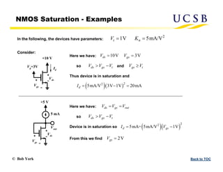
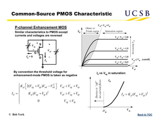
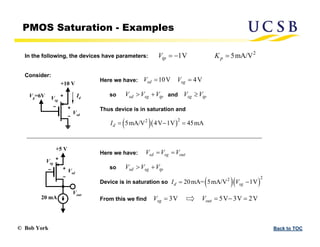
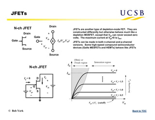
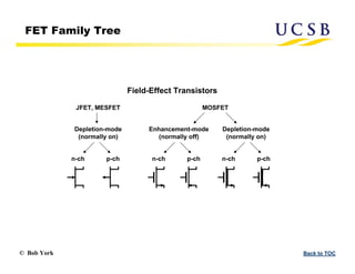
© Bob York
Transistor Basics - MOSFETs
© Bob York Back to TOC
Transistors, Conceptually
Control
Terminal
I(V)
I(V, Vc)
I(V, Ic)
or
V
V
Vc or Ic
FETs
BJTs
So far we have considered two-terminal devices that are described by a
current-voltage relationship I=f(V)
Transistors add a third terminal to control the current flow through the device.
The two most common types of transistors are:
• Field-Effect Transistors (FETs):
voltage-controlled current flow
• Bipolar Junction Transistors (BJTs):
current-controlled current flow
In ECE 2, we will not discuss the physics of device operation in depth.
The transistor is simply a black box with certain well-defined terminal properties.
• Resistors:
• Capacitors:
• Inductors:
• Diodes:
/
I V R

dV
dt
I C

1
L
I Vdt

 /
1
T
V nV
s
I I e
 
 
 
© Bob York Back to TOC
MOSFETs
Vgs
Gate
Source
Drain
Ids(Vgs,Vds)
Vds
Id
Vgs
Vds
Ig ≈ 0
Gate
Source
Drain
G
D
S
NMOS
There are many types of FETs but all share some
common features and nomenclature.
Key points:
• Every FET has a gate, drain, and source
• Current flows between the drain and source.
• The gate is the control terminal.
• The DC gate “leakage” current is negligible, Ig≈0
Start with n-channel enhancement MOS (NMOS)
(MOS=Metal-Oxide-Semiconductor).
If we take the source as the voltage reference
(ground), the drain current will depend on the
gate voltage and drain voltage as shown :
Vgs
Vds
Id
Current-Voltage Characteristic for NMOS
D
ra
in
C
u
rr
e
n
t
Drain Voltage
Gate
Voltage
“Common-source” configuration
© Bob York Back to TOC
Common-Source NMOS Characteristic
Saturation region
ID
Ohmic or
Triode region
Vds
Vgs= Vtn + 0.5
Vgs= Vtn + 1.0
Vgs= Vtn + 1.5
Vgs= Vtn + 2.0
Increasing
V
gs
Id vs Vds for specific values of Vgs
Vds= Vgs-Vt
Vgs ≤ Vtn (cutoff)
Id
Vgs
Vds
Ig = 0
G
D
S
Id
Vgs
Vds
Ig = 0
G
D
S
ID
Vgs
Vt
Important observations:
• No current flows for Vgs< Vtn. Vtn is called the
“Threshold voltage”
• Once the drain voltage exceeds Vgs-Vtn, a
constant current flows that depends on Vgs
• For enhancement-mode NMOS the gate
threshold voltage is positive Vtn>0
Device
is
“off”
no
current
flows
Id vs Vgs in saturation:
2
2
2( )
( )
0
n gs tn ds ds ds gs tn
d n gs tn ds gs tn
gs tn
K V V V V V V V
I K V V V V V
V V
  
   
 


   


 

ds gs tn
V V V
 
I-V Curves are described analytically by:
2
( )
d n gs tn
I K V V
 
N-channel Enhancement MOS
© Bob York Back to TOC
MOSFET Saturation Region
 
2
d n gs t
I K V V
 
The saturation region is especially important.
The NMOS device is in saturation when the following conditions are satisfied:
 
d n gs t
I K V V

 
ds gs t
V V V
  gs t
V V

When the device is in saturation the drain current is given by:
Kn and Vt are the important device parameters.
Kn depends on some material constants and
the device size/geometry
It is difficult to control Kn and Vt precisely, so
two different discrete devices may have
significant differences in these parameters
Later we will explore some circuit techniques
to deal with this issue
Note: state-of-the-art devices may follow a different behavior:
where α is closer to 1
ID
Vgs
Vt1 Vt2
Device #1
Device #2
© Bob York Back to TOC
NMOS Saturation - Examples
Vg=3V Id
+10 V
Vout
5 mA
+5 V
2
1V 5mA/V
t n
V K
 
In the following, the devices have parameters:
Consider:
  2
2
5mA/V 3V 1V 20mA
d
I   
10V
ds
V 
Here we have: 3V
gs
V 
so ds gs t
V V V
  gs t
V V

and
Thus device is in saturation and
  
2
2
5mA= 5mA/V 1V
d gs
I V
 
ds gs out
V V V
 
Here we have:
so ds gs t
V V V
 
Device is in saturation so
From this we find 2V
gs
V 
Vgs
Vds
Vgs
Vds
© Bob York Back to TOC
Common-Source PMOS Characteristic
P-channel Enhancement MOS
Similar characteristics to PMOS except
currents and voltages are reversed
Saturation region
ID
Ohmic or
Triode region
Vsd
Vsg= Vtp + 0.5
Vsg= Vtp + 1.0
Vsg= Vtp + 1.5
Vsg= Vtp + 2.0
Increasing
V
sg
Vsd= Vsg+Vtp
Vsg ≤ Vtp (cutoff)
ID
Vsg
-Vtp
Device
is
“off”
no
current
flows
Id vs Vsg in saturation:
Id
Vsg
Vsd
Ig = 0
G
D
S
By convention the threshold voltage for
enhancement-mode PMOS is taken as negative
2
2
2( )
( )
0
p sg tp sd sd sd sg tp
d p sg tp sd sg tp
sg tp
K V V V V V V V
I K V V V V V
V V
  
   
 


   


 

2
( )
d p sg tp
I K V V
 
© Bob York Back to TOC
PMOS Saturation - Examples
Vg=6V Id
+10 V
2
1V 5mA/V
tp p
V K
  
In the following, the devices have parameters:
Consider:
  2
2
5mA/V 4V 1V 45mA
d
I   
10V
sd
V 
Here we have: 4V
sg
V 
so sd sg tp
V V V
  sg tp
V V

and
Thus device is in saturation and
  
2
2
20mA= 5mA/V 1V
d sg
I V
 
sd sg out
V V V
 
Here we have:
so sd sg tp
V V V
 
Device is in saturation so
From this we find 3V
sg
V 
Vout
20 mA
+5 V
5V 3V 2V
out
V   
Vsg
Vsd
Vsg
Vsd
© Bob York Back to TOC
Depletion-Mode FETs
Enhancement-mode devices are “normally off” devices, since no current flows when Vgs=0. A
certain applied gate voltage is required to “turn on” the device and get current flowing
Depletion-mode devices are “normally on”. They conduct current at Vgs=0, and an applied
gate voltage is required to stop the current flow and turn them “off”
ID
Vgs
Device
is
“off”
no
current
flows
2
( )
d n gs tn
I K V V
 
Id
Vgs
Vds
Ig = 0
G
D
S
N-channel Depletion-mode MOS
symbol
Vtn
Id vs Vgs in saturation:
Threshold
voltage has the
opposite sign in
comparison to
enhancement
devices.
Otherwise the
characteristics
are similar.
dss
I
P-channel Depletion-mode MOS
Id
Vsg
Vsd
Ig = 0
G
D
S
symbol
ID
Vsg
-Vtp
Device
is
“off”
no
current
flows
Id vs Vsg in saturation:
2
( )
d p sg tp
I K V V
 
dss
I
© Bob York Back to TOC
MOSFET Construction
Semiconducting substrate
Lg
Source Drain
Gate
“Body” connection
Gate oxide
Wg
Key parameters: :gate length : gate width
: oxide capacitance density
: carrier mobility in semiconductor
g g
ox
L W
c

Enhancement Devices
No charge carriers exist
under the gate, so no
current flow is possible
An applied field allows
charge to accumulate
under the gate allowing
current to flow
0
gs
V  gs t
V V

Depletion Devices
Charge carriers
naturally accumulate
under the gate, allowing
current to flow
The applied field
depletes the charge in
the channel, cutting off
the flow of current
0
gs
V  gs t
V V

1 1 1 1
2 2 2 2
g g g g
n n ox n p p ox p
g g g g
W W W W
K c k K c k
L L L L
 
 
   
Saturation current parameter:
N-channel P-channel
Engineers control whether a device is an enhancement or depletion device by adding
carefully-controlled amounts of impurities (‘dopants”) in the semiconductor
© Bob York Back to TOC
JFETs
Vgs
Gate
Source
Drain
Ids(Vgs,Vds)
Vds
Id
Vgs
Vds
Ig = 0
Gate
Source
Drain
Saturation region
ID
Vgs ≤ Vt (cutoff)
Ohmic or
Triode region
Vds
Vgs= Vt + 0.5
Vgs= Vt + 1.0
Vgs= Vt + 1.5
Vgs= 0
G
D
S
Idss
Increasing
V
gs
N-ch JFET
N-ch JFET
JFETs are another type of depletion-mode FET. They are
constructed differently but otherwise behave much like a
depletion MOSFET, except that Vgs can never exceed zero
volts. The maximum current at Vgs=0 is Idss.
JFETs can be made in both n-channel and p-channel
versions. Some high-speed compound semiconductor
devices (GaAs MESFETs and HEMTs) behave like JFETs
© Bob York Back to TOC
FET Family Tree
Field-Effect Transistors
JFET, MESFET
Depletion-mode
(normally on)
n-ch p-ch
MOSFET
Depletion-mode
(normally on)
Enhancement-mode
(normally off)
n-ch p-ch n-ch p-ch
© Bob York Back to TOC
Discrete Device Example: 2N7000
2N7000
0
20
40
60
80
100
120
2.2 2.4 2.6 2.8 3.0 3.2
Vgs, Volts
Id,
mA
Data
Model
2
2.35V
220mA/V
t
n
V
K


This is a popular discrete NMOS device
that we will use in the ECE 2 lab.
From the data sheet:
ID
Gate
Source
Drain
Vgs
A
Vds
2N7000
Vds
ID
Gate
Source
Drain
Vgs
A
Vds
2N7000
Vds
Measured Data
The data sheet specifies that Vt is between
0.8V and 3V, with a typical value of 2.1V.
Such a wide range of expected Vt is typical
of many discrete devices.
Representative data for small currents is
shown at left

Transisotor-MOSFETS Basics Operation.pdf

  • 1.
    © Bob York TransistorBasics - MOSFETs
  • 2.
    © Bob YorkBack to TOC Transistors, Conceptually Control Terminal I(V) I(V, Vc) I(V, Ic) or V V Vc or Ic FETs BJTs So far we have considered two-terminal devices that are described by a current-voltage relationship I=f(V) Transistors add a third terminal to control the current flow through the device. The two most common types of transistors are: • Field-Effect Transistors (FETs): voltage-controlled current flow • Bipolar Junction Transistors (BJTs): current-controlled current flow In ECE 2, we will not discuss the physics of device operation in depth. The transistor is simply a black box with certain well-defined terminal properties. • Resistors: • Capacitors: • Inductors: • Diodes: / I V R  dV dt I C  1 L I Vdt   / 1 T V nV s I I e      
  • 3.
    © Bob YorkBack to TOC MOSFETs Vgs Gate Source Drain Ids(Vgs,Vds) Vds Id Vgs Vds Ig ≈ 0 Gate Source Drain G D S NMOS There are many types of FETs but all share some common features and nomenclature. Key points: • Every FET has a gate, drain, and source • Current flows between the drain and source. • The gate is the control terminal. • The DC gate “leakage” current is negligible, Ig≈0 Start with n-channel enhancement MOS (NMOS) (MOS=Metal-Oxide-Semiconductor). If we take the source as the voltage reference (ground), the drain current will depend on the gate voltage and drain voltage as shown : Vgs Vds Id Current-Voltage Characteristic for NMOS D ra in C u rr e n t Drain Voltage Gate Voltage “Common-source” configuration
  • 4.
    © Bob YorkBack to TOC Common-Source NMOS Characteristic Saturation region ID Ohmic or Triode region Vds Vgs= Vtn + 0.5 Vgs= Vtn + 1.0 Vgs= Vtn + 1.5 Vgs= Vtn + 2.0 Increasing V gs Id vs Vds for specific values of Vgs Vds= Vgs-Vt Vgs ≤ Vtn (cutoff) Id Vgs Vds Ig = 0 G D S Id Vgs Vds Ig = 0 G D S ID Vgs Vt Important observations: • No current flows for Vgs< Vtn. Vtn is called the “Threshold voltage” • Once the drain voltage exceeds Vgs-Vtn, a constant current flows that depends on Vgs • For enhancement-mode NMOS the gate threshold voltage is positive Vtn>0 Device is “off” no current flows Id vs Vgs in saturation: 2 2 2( ) ( ) 0 n gs tn ds ds ds gs tn d n gs tn ds gs tn gs tn K V V V V V V V I K V V V V V V V                     ds gs tn V V V   I-V Curves are described analytically by: 2 ( ) d n gs tn I K V V   N-channel Enhancement MOS
  • 5.
    © Bob YorkBack to TOC MOSFET Saturation Region   2 d n gs t I K V V   The saturation region is especially important. The NMOS device is in saturation when the following conditions are satisfied:   d n gs t I K V V    ds gs t V V V   gs t V V  When the device is in saturation the drain current is given by: Kn and Vt are the important device parameters. Kn depends on some material constants and the device size/geometry It is difficult to control Kn and Vt precisely, so two different discrete devices may have significant differences in these parameters Later we will explore some circuit techniques to deal with this issue Note: state-of-the-art devices may follow a different behavior: where α is closer to 1 ID Vgs Vt1 Vt2 Device #1 Device #2
  • 6.
    © Bob YorkBack to TOC NMOS Saturation - Examples Vg=3V Id +10 V Vout 5 mA +5 V 2 1V 5mA/V t n V K   In the following, the devices have parameters: Consider:   2 2 5mA/V 3V 1V 20mA d I    10V ds V  Here we have: 3V gs V  so ds gs t V V V   gs t V V  and Thus device is in saturation and    2 2 5mA= 5mA/V 1V d gs I V   ds gs out V V V   Here we have: so ds gs t V V V   Device is in saturation so From this we find 2V gs V  Vgs Vds Vgs Vds
  • 7.
    © Bob YorkBack to TOC Common-Source PMOS Characteristic P-channel Enhancement MOS Similar characteristics to PMOS except currents and voltages are reversed Saturation region ID Ohmic or Triode region Vsd Vsg= Vtp + 0.5 Vsg= Vtp + 1.0 Vsg= Vtp + 1.5 Vsg= Vtp + 2.0 Increasing V sg Vsd= Vsg+Vtp Vsg ≤ Vtp (cutoff) ID Vsg -Vtp Device is “off” no current flows Id vs Vsg in saturation: Id Vsg Vsd Ig = 0 G D S By convention the threshold voltage for enhancement-mode PMOS is taken as negative 2 2 2( ) ( ) 0 p sg tp sd sd sd sg tp d p sg tp sd sg tp sg tp K V V V V V V V I K V V V V V V V                     2 ( ) d p sg tp I K V V  
  • 8.
    © Bob YorkBack to TOC PMOS Saturation - Examples Vg=6V Id +10 V 2 1V 5mA/V tp p V K    In the following, the devices have parameters: Consider:   2 2 5mA/V 4V 1V 45mA d I    10V sd V  Here we have: 4V sg V  so sd sg tp V V V   sg tp V V  and Thus device is in saturation and    2 2 20mA= 5mA/V 1V d sg I V   sd sg out V V V   Here we have: so sd sg tp V V V   Device is in saturation so From this we find 3V sg V  Vout 20 mA +5 V 5V 3V 2V out V    Vsg Vsd Vsg Vsd
  • 9.
    © Bob YorkBack to TOC Depletion-Mode FETs Enhancement-mode devices are “normally off” devices, since no current flows when Vgs=0. A certain applied gate voltage is required to “turn on” the device and get current flowing Depletion-mode devices are “normally on”. They conduct current at Vgs=0, and an applied gate voltage is required to stop the current flow and turn them “off” ID Vgs Device is “off” no current flows 2 ( ) d n gs tn I K V V   Id Vgs Vds Ig = 0 G D S N-channel Depletion-mode MOS symbol Vtn Id vs Vgs in saturation: Threshold voltage has the opposite sign in comparison to enhancement devices. Otherwise the characteristics are similar. dss I P-channel Depletion-mode MOS Id Vsg Vsd Ig = 0 G D S symbol ID Vsg -Vtp Device is “off” no current flows Id vs Vsg in saturation: 2 ( ) d p sg tp I K V V   dss I
  • 10.
    © Bob YorkBack to TOC MOSFET Construction Semiconducting substrate Lg Source Drain Gate “Body” connection Gate oxide Wg Key parameters: :gate length : gate width : oxide capacitance density : carrier mobility in semiconductor g g ox L W c  Enhancement Devices No charge carriers exist under the gate, so no current flow is possible An applied field allows charge to accumulate under the gate allowing current to flow 0 gs V  gs t V V  Depletion Devices Charge carriers naturally accumulate under the gate, allowing current to flow The applied field depletes the charge in the channel, cutting off the flow of current 0 gs V  gs t V V  1 1 1 1 2 2 2 2 g g g g n n ox n p p ox p g g g g W W W W K c k K c k L L L L         Saturation current parameter: N-channel P-channel Engineers control whether a device is an enhancement or depletion device by adding carefully-controlled amounts of impurities (‘dopants”) in the semiconductor
  • 11.
    © Bob YorkBack to TOC JFETs Vgs Gate Source Drain Ids(Vgs,Vds) Vds Id Vgs Vds Ig = 0 Gate Source Drain Saturation region ID Vgs ≤ Vt (cutoff) Ohmic or Triode region Vds Vgs= Vt + 0.5 Vgs= Vt + 1.0 Vgs= Vt + 1.5 Vgs= 0 G D S Idss Increasing V gs N-ch JFET N-ch JFET JFETs are another type of depletion-mode FET. They are constructed differently but otherwise behave much like a depletion MOSFET, except that Vgs can never exceed zero volts. The maximum current at Vgs=0 is Idss. JFETs can be made in both n-channel and p-channel versions. Some high-speed compound semiconductor devices (GaAs MESFETs and HEMTs) behave like JFETs
  • 12.
    © Bob YorkBack to TOC FET Family Tree Field-Effect Transistors JFET, MESFET Depletion-mode (normally on) n-ch p-ch MOSFET Depletion-mode (normally on) Enhancement-mode (normally off) n-ch p-ch n-ch p-ch
  • 13.
    © Bob YorkBack to TOC Discrete Device Example: 2N7000 2N7000 0 20 40 60 80 100 120 2.2 2.4 2.6 2.8 3.0 3.2 Vgs, Volts Id, mA Data Model 2 2.35V 220mA/V t n V K   This is a popular discrete NMOS device that we will use in the ECE 2 lab. From the data sheet: ID Gate Source Drain Vgs A Vds 2N7000 Vds ID Gate Source Drain Vgs A Vds 2N7000 Vds Measured Data The data sheet specifies that Vt is between 0.8V and 3V, with a typical value of 2.1V. Such a wide range of expected Vt is typical of many discrete devices. Representative data for small currents is shown at left