
Recommended
More Related Content
What's hot
What's hot (20)
Similar to Metal Insulator Semiconductor devices
Similar to Metal Insulator Semiconductor devices (20)
More from utpal sarkar
More from utpal sarkar (20)
Recently uploaded
Recently uploaded (20)
Metal Insulator Semiconductor devices
- 2. Importance for LSI/VLSI Low fabrication cost Small size Low power consumption Applications Microprocessors Memories Power Devices Basic Properties Unipolar device Very high input impedance Capable of power gain 3/4 terminal device, G, S, D, B Two possible device types: enhancement mode; depletion mode Two possible channel types: n-channel; p-channel
- 3. Transistors These are three terminal devices, where the current or voltage at one terminal, the input terminal, controls the flow of current between the two remaining terminals.
- 4. FETs Two primary types: MOSFET, Metal-Oxide-Semiconductor FET. Also known as IGFET – Insulated Gate FET; JFET, Junction FET. MOS transistors can be: n-Channel; Enhancement mode; Depletion mode; p-Channel; Enhancement mode; Depletion mode;
- 5. Different types of FETs Metal-Semiconductor FET (MESFET)
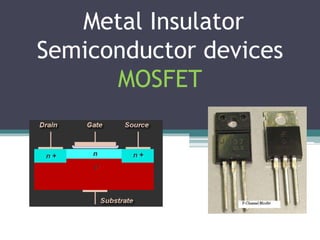
- 7. MOSFET Structure p-Si n+ L Source Gate Drain Field Oxide Gate Oxide Bulk (Substrate)
- 8. MOSFET (n-channel Enhancement-Mode) Device Structure Substrate, source connected to ground The drain-body n+p junction is reverse-biased. The body-source pn+ junction is reverse-biased. Enhancement MOSFET acts as an open circuit with no gate voltage.
- 10. MOSFET Operation • Voltage at gate controls the flow of current between drain and source. • VGS – Voltage between gate and source. • VDS – Voltage between drain and source.
- 11. MOSFET Operation • When VGS = 0 then no current flows between drain and source. • pn-Junction is reverse biased.
- 12. Basic MOSFET (n-channel) • The gate electrode is placed on top of a very thin insulating layer. • There are a pair of small n- type regions just under the drain & source electrodes. • If apply a +ve voltage to gate, will push away the ‘holes’ inside the p-type substrate and attracts the moveable electrons in the n-type regions under the source & drain electrodes.
- 13. Basic MOSFET (n-channel) • Increasing the +ve gate voltage pushes the p-type holes further away and enlarges the thickness of the created channel. • As a result increases the amount of current which can go from source to drain — this is why this kind of transistor is called an enhancement mode device.
- 14. Carbon N-TE-DNA BioFET Whole Cell SummaryIntroduction FET Drain Gate Source - - - - - - Insulator + + + + + (Electron Channel) (Not conductive enough)
- 15. Carbon N-TE-DNA BioFET Whole Cell SummaryIntroduction FET Drain Gate Source - Insulator + + + + + Threshold Voltage
- 16. Carbon N-TE-DNA BioFET Whole Cell SummaryIntroduction FET Drain Gate Source - - - - - - - - Insulator + + + + + + + + + - -- -- -
- 17. Note the n-type body and the p- type source and drain areas. Both VGS and VDD are negative with respect to ground.
- 18. January 2004ELEC 121 19 n-Channel E-MOSFET showing channel length L and channel width W
- 19. A family of curves representing the V-I characteristics of transistors. A plot of drain current, ID, as a function of drain- to-source voltage, VDS, for several values of VGS.
- 20. Depletion Mode MOSFETs • n-Channel is built in. • VGS varies from negative values to positive values, where negative values of VGS depletes the channel while positive values enhance it further.
- 21. January 2004 ELEC 121 22 D-MOSFET Depletion Mode Operation The transfer characteristics are similar to the JFET In Depletion Mode operation: When VGS = 0V, ID = IDSS When VGS < 0V, ID < IDSS When VGS > 0V, ID > IDSS The formula used to plot the Transfer Curve, is: 2 GS D DSS P V I = I 1- V
- 22. September 17, 2007 23 The enhancement-type NMOS transistor with a positive voltage applied to the gate. An n channel is induced at the top of the substrate beneath the gate. Operation
- 23. September 17, 2007 24 vGS > Vt ,small vDS applied. the channel conductance is proportional to vGS - Vt, and is proportional to (vGS - Vt) vDS. Triode Region
- 24. September 17, 2007 25 The induced channel acquires a tapered shape and its resistance increases as vDS is increased. vGS > Vt. Saturation Region
- 25. September 17, 2007 26 Derivation of the iD - vDS characteristic of the NMOS transistor.
- 26. September 17, 2007 27 Increasing vDS beyond vDSsat causes the channel pinch-off point to move slightly away from the drain, thus reducing the effective channel length (by L).
- 27. September 17, 2007 28 Enhancement-type NMOS transistor operated with vGS > Vt. Drain current iD versus vDS
- 28. ECE 663 Drain current for REALLY small VD TGD DTGinD DDTGinD VVV VVVC L Z I VVVVC L Z I 2 2 1 Linear operation Channel Conductance: )( TGin VD D D VVC L Z V I g G Transconductance: Din VG D m VC L Z V I g D
- 29. ECE 663 In Saturation • Channel Conductance: • Transconductance: 2 2 TGinD VVC L Z satI 0 GVD D D V I g TGin VG D m VVC L Z V I g D
- 30. January 2004 ELEC 121 31 Summary Table JFET D-MOSFET E-MOSFET
- 31. I-V Characteristics of MOSFET
- 32. CMOS Circuit
- 33. September 17, 2007 34 Cross section of a CMOS integrated circuit. Note that the PMOS transistor is formed in a separate n-type region, known as an n well. Another arrangement is also possible in which an n-type body is used and the n device is formed in a p well.
- 34. Fabrication and Layout Slide 35 Transistors as Switches • We can view MOS transistors as electrically controlled switches • Voltage at gate controls path from source to drain g s d g = 0 s d g = 1 s d g s d s d s d nMOS pMOS OFF ON ON OFF
- 35. Fabrication and Layout Slide 36 CMOS Inverter A Y 0 1 VDD A Y GND A Y
- 36. Fabrication and Layout Slide 37 CMOS Inverter A Y 0 1 0 VDD A=1 Y=0 GND ON OFF A Y
- 37. Fabrication and Layout Slide 38 CMOS Inverter A Y 0 1 1 0 VDD A=0 Y=1 GND OFF ON A Y
- 38. MOS (complementary metal oxide semiconductor) logic has a few desirable advantages: • High input impedance. The input signal is driving electrodes with a layer of insulation (the metal oxide) between them and what they are controlling. This gives them a small amount of capacitance, but virtually infinite resistance. The current into or out of CMOS input held at one level is just leakage, usually 1 nanoAmpere or less • CMOS logic takes very little power when held in a fixed state. The current consumption comes from switching as those capacitors are charged and discharged. Even then, it has good speed to power ratio compared to other logic types. • CMOS gates are very simple. The basic gate is an inverter, which is only two transistors. This together with the low power consumption means it lends itself well to dense integration. Or conversely, you get a lot of logic for the size, cost and power.
- 39. Few Applications
- 40. 41 CCD Image Sensors • High QE and low dark current • Serial readout: – Slow readout – Complex clocking and supply requirements – High power consumption • Cannot integrate circuitry on chip
- 41. 42 CMOS Image Sensors • Memory-like readout: – Enables high speed operation – Low power consumption – Region of interest • Integration • Enable new applications: – Embedded imaging – High dynamic range – Biometrics – 3D imaging Column Amplifiers / Caps Column ADC / Mux RowDecoder Pixel Word Bit Reset Word Bit
- 42. 43 Image Sensor Market 0 20,000 40,000 60,000 80,000 100,000 120,000 140,000 160,000 180,000 200,000 2001 2002 2003 2004 2005 2006 Year ThousandsofUnits CMOS CCD Source: In-Stat/MDR, 8/02
- 43. 44 Technology and Design Trends • Recent developments in: – Silicon processing – Color Filter Array and Microlens – Miniaturized packaging – Pixel design – Camera-on-chip • Promise to broaden CMOS image sensor applicability and enhance their performance
- 44. 45 Problems with standard CMOS • Low photoresponsivity -- shallow junctions, high doping • High junction leakage -- STI, salicide • High transistor leakage – off-current, thin gate oxide • Poor analog circuit performance Wong IEDM’96
- 49. Carbon N-TE-DNA BioFET Whole Cell SummaryIntroduction BioFET • Draws upon versatility of common electronic component (Field-Effect Transistor) • Well understood expectations/results
- 50. Carbon N-TE-DNA BioFET Whole Cell SummaryIntroduction Source: Im et al., 2007 BioFET
- 51. Carbon N-TE-DNA BioFET Whole Cell SummaryIntroduction Source: Im et al., 2007 BioFET
- 52. Carbon N-TE-DNA BioFET Whole Cell SummaryIntroduction Source: Im et al., 2007 BioFET Results Gate (before)
- 53. Carbon N-TE-DNA BioFET Whole Cell SummaryIntroduction Source: Im et al., 2007 BioFET Results Gate (after etch, w/biotin) Gate (w/ complete Biomolecule) d
- 54. Thank You