14827 mosfet
•Download as PPT, PDF•
7 likes•5,565 views

The document discusses the metal-oxide-semiconductor field-effect transistor (MOSFET). It describes the basic structure of the MOSFET, including the source, gate, and drain terminals. It also discusses the different types of MOSFETs, such as n-channel and p-channel MOSFETs, as well as depletion and enhancement MOSFETs. The key characteristics of MOSFETs are summarized, including the different regions of operation depending on the voltages applied to the gate, source, and drain terminals. Common applications of MOSFETs in analog and digital circuits are also outlined.

Recommended
More Related Content
What's hot
What's hot (20)
Viewers also liked
Viewers also liked (18)
Similar to 14827 mosfet
Similar to 14827 mosfet (20)
More from Sandeep Kumar
Recently uploaded
Recently uploaded (20)
14827 mosfet
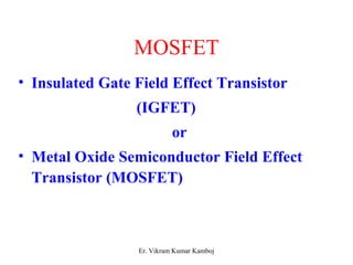
- 1. MOSFET • Insulated Gate Field Effect Transistor (IGFET) or • Metal Oxide Semiconductor Field Effect Transistor (MOSFET) Er. Vikram Kumar Kamboj
- 2. Types of MOSFET • 1. Depletion MOSFET (D-MOSFET) • 2. Enhancement MOSFET(E-MOSFET) • 3. Depletion-Enhancement MOSFET (DE-MOSFET) Er. Vikram Kumar Kamboj
- 3. Types (According to Channel) • P-Channel MOSFET • N-Channel MOSFET Er. Vikram Kumar Kamboj
- 4. MOSFET Structure Source Gate Drain n+ L p-Si Gate Oxide Field Oxide Bulk (Substrate) Er. Vikram Kumar Kamboj
- 5. Symbols G D S B G D S B p Channel MOSFET n Channel MOSFET Er. Vikram Kumar Kamboj
- 6. MOSFET Symbols gate body A circle is sometimes used on the gate terminal to show active low input drain gate body source or or drain gate body source drain source drain gate body source A) n-channel MOSFET B) p-channel MOSFET Er. Vikram Kumar Kamboj
- 7. DE-MOSFET symbol Er. Vikram Kumar Kamboj
- 8. Comparison of Symbols Er. Vikram Kumar Kamboj
- 9. Metal Oxide Semiconductor Field Effect Transistor Simplified Schematic of a MOSFET The MOSFET shown in the adjacent figure is an n-channel MOSFET, in which electrons flow from source to drain in the channel induced under the gate oxide. Both n-channel and p-channel MOSFETs are extensively used. In fact, CMOS IC technology relies on the ability to use both devices on the same chip. The table below shows the dopant types used in each region of the two structures. n-channel MOSFET p-channel MOSFET Substrate (Channel) p N Gate Electrode n+ p+ Source and Drain n+ p+ Er. Vikram Kumar Kamboj
- 10. Physical Structure of MOS FETS NMOS PMOS Er. Vikram Kumar Kamboj [Adapted from Principles of CMOS VLSI Design by Weste & Eshraghian]
- 11. Device Operation Schematic Figure shows an n-channel MOSFET with voltages applied to its four terminals. Typically, VS = VB and VD > VS. For simplicity, we assume that the body and the source terminals are tied to the ground, ie. VSB=0. This yields VGS = VGB - VSB = VGB = VG VDS = VDB - VSB = VDB = VD Er. Vikram Kumar Kamboj
- 12. SiO2 Insulator (Glass) Gate Source Drain holes electrons 5 volts electrons to be transmitted MOSFET Operation Step 1: Apply Gate Voltage N N Step 2: Excess electrons surface in channel, holes are repelled. Step 3: Channel becomes saturated with electrons. Electrons in source are able to flow across channel to Drain. P Er. Vikram Kumar Kamboj
- 13. Regions of MOSFET Operation Er. Vikram Kumar Kamboj
- 14. Off-State Region • With a small positive voltage on the drain and no bias on the gate • i.e. VDS > 0 and VGS = 0, the drain is a reverse biased pn junction • Conduction band electrons in the source region encounter a potential barrier determined by the built-in potential of the source junction • As a result electrons cannot enter the channel region and hence, no current flows from the source to the drain • This is referred to as the “off” state Er. Vikram Kumar Kamboj
- 15. Linear Region •With a small positive bias on the gate, electrons can enter the channel and a current flow from source to drain is established •In the low drain bias regime, the drain current increases almost linearly with drain bias •Indeed, here the channel resembles an ideal resistor obeying Ohm’s law •The channel resistance is determined by the electron concentration in the channel, which is a function of the gate bias •Therefore, the channel acts like a voltage controlled resistor whose resistance is determined by the applied gate bias •As the gate bias is increased, the slope of the I-V characteristic gradually increases due to the increasing conductivity of the channel •We obtain different slopes for different gate biases •This region where the channel behaves like a resistor is referred to as the linear region of operation •The drain current in the linear regime is given by ù 1 I W m = ¢ é - - 2 ( ) úû D lin ox GS T DS DS C V V V V êë , L 2 Er. Vikram Kumar Kamboj
- 16. Saturation Region For larger drain biases, the drain current saturates and becomes independent of the drain bias Naturally, this region is referred to as the saturation region The drain current in saturation is derived from the linear region current, which is a parabola with a maximum occurring at VD,sat given by VD,sat = VGS - VT a To obtain the drain current in saturation, this VD,sat value can be substituted in the linear region expression, which gives ( ) C V V I = W m ¢ - 2 2 , GS T D sat ox L Er. Vikram Kumar Kamboj
- 17. FET output characteristics Er. Vikram Kumar Kamboj
- 18. Current-Voltage Characteristic I B C D DS A VDS Er. Vikram Kumar Kamboj
- 19. Transfer characteristics – similar shape for all forms of FET – but with a different offset – not a linear response, but over a small region might be considered to approximate a linear response Er. Vikram Kumar Kamboj
- 20. Normal operating ranges for FETs Er. Vikram Kumar Kamboj
- 21. • When operating about its operating point we can describe the transfer characteristic by the change in output that is caused by a certain change in the input – this corresponds to the slope of the earlier curves – this quantity has units of current/voltage, which is the reciprocal of resistance (this is conductance) – since this quantity described the transfer characteristics g = D I D it is called g the ¹ I D m transconductance, D V m GS gV GS m Er. Vikram Kumar Kamboj
- 22. • Small-signal equivalent circuit of a FET – models the behaviour of the device for small variations of the input about the operating point Er. Vikram Kumar Kamboj
- 23. Summary of FET Characteristics • FETS have three terminals: drain, source and gate • The gate is the control input • Two polarities of device: n-channel and p-channel 20.6 • Two main forms of FET: MOSFET and JFET • In each case the drain current is controlled by the voltage applied to the gate with respect to Er. Vikram Kumar Kamboj the source
- 24. Applications Er. Vikram Kumar Kamboj
- 25. FET Amplifiers • A simple DE MOSFET amplifier – RG is used to ‘bias’ the gate at its correct operating point (which for a DE MOSFET is 0 V) – C is a coupling capacitor and is used to couple the AC signal while preventing externals circuits from affecting the bias – this is an AC-coupled amplifier 20.7 Er. Vikram Kumar Kamboj
- 26. • AC-coupled amplifier – input resistance – equal to RG – output resistance – approximately equal to RD – gain – approximately –gmRD (the minus sign shows that this is an inverting amplifier) – C produced a low-f = frequency 1 cut-off at a frequency fgiven c by 2pCR c where R is the Er. input Vikram Kumar resistance Kamboj of the amplifier (which in this case is equal to R)
- 27. • Negative feedback amplifier – reduces problems of variability of active components – voltage across Rs is proportional to drain current, which is directly proportional to the output voltage – this voltage is subtracted from input voltage to gate – hence negative feedback Er. Vikram Kumar Kamboj
- 28. • Source follower – similar to earlier circuit, but output is now taken from the source – feedback causes the source to follow the input voltage – produces a unity-gain amplifier – also called a source follower Er. Vikram Kumar Kamboj
- 29. Other FET Applications • A voltage controlled attenuator – for small drain-to-source voltages FETs resemble voltage-controlled resistors – the gate voltage VG is used to control this resistance and hence the gain of the potential divider – used, for example, in automatic gain control in radio receivers 20.8 Er. Vikram Kumar Kamboj
- 30. • A FET as an analogue switch Er. Vikram Kumar Kamboj
- 31. • A FET as a logical switch Er. Vikram Kumar Kamboj
- 32. Key Points • FETs are widely used in both analogue and digital circuits • They have high input resistance and small physical size • There are two basic forms of FET: MOSFETs and JFETs • MOSFETs may be divided into DE and Enhancement types • In each case the gate voltage controls the current from the drain to the source • The characteristics of the various forms of FET are similar except that they require different bias voltages • The use of coupling capacitors prevents the amplification of DC and produced AC amplifiers • FETs can be used to produce various forms of amplifier and a range of other circuit applications Er. Vikram Kumar Kamboj
- 33. • Importance for LSI/VLSI – Low fabrication cost – Small size – Low power consumption • Applications – Microprocessors – Memories – Power Devices • Basic Properties – Unipolar device – Very high input impedance – Capable of power gain – 3/4 terminal device, G, S, D, B – Two possible device types: enhancement mode; depletion mode – Two possible channel types: n-channel; p-channel Er. Vikram Kumar Kamboj
- 34. Analysis: Low VDS (A) I Q DS n TR = - t Q t t L v n TR v d d = = = = Channel Charge Channel Transit Time Drift Velocity TR m L V n DS = 2 Q CV = = - ( - ) C V V WL n O GS T I C V V WL m ( - ) n O GS T V DS = 2 DS L I W L C V V V DS n O GS T DS = m ( - ) Er. Vikram Kumar Kamboj
- 35. Analysis: Intermediate VDS Q C V V DS = - ( - - V ) WL n O G T 2 First Order Approximation Gate to Channel Voltage = VGS-VDS/2 I W L C V V V V W L C V V V V DS n O G T DS DS n O G T DS 2 DS = æè ç öø ÷ - - æè ç öø ÷ = æè ç öø ÷ - - æ è ç ö ø ÷ m m 2 2 ( ) Extra term! Er. Vikram Kumar Kamboj
- 36. Large VDS: Saturation (C) Source Channel Drain VG VDS VT VG-channel Pinch-off Er. Vikram Kumar Kamboj
- 37. Analysis: Saturation (C) Pinch-off V sat V V DS G T ( ) = - Substitute for VDS(sat) in equation for IDS to get IDS(sat) I W L æ = C V V V æè ç DS V öø ÷ - - è ç DS n O GS T DS ö ø ÷ m ( ) 2 2 æ - ( ) ( ) DS n O GS T ( ) I sat W L C V V V V W L C V V GS DS n O GS T ( ) = æè ç öø ÷ - - è ç ö ø ÷ = æè ç öø ÷ - = m m 2 2 2 2 2 constant Er. Vikram Kumar Kamboj
- 38. Avalanche and Punch-Through (D) • For very large VDS, IDS increases rapidly due to drain junction avalanche. • Can give rise to parasitic bipolar action. • In short channel transistors, the drain depletion region may reach the source depletion region giving rise to ‘Punch Through’. Er. Vikram Kumar Kamboj
Editor's Notes
- Structure p-type Silicon substrate n+ ion implanted source and drain regions High quality (thin) gate oxide (dry process) Overlaps slightly source and drain regions Thick field oxide Protection + carries contact tracks Channel Region between source and drain and under gate. Enhancement Mode MOSFET n-channel with VG>VT Semiconductors:Si; Ge; GaAs Insulators:SiO3; Si3N4; Al2O3 Most Important Combination:Si/SiO2 Typical Dimensions Long channel MOSFET L>>WS, WD L ~ 5m Oxide Thickness 50-100nm
- Analysis MOSFET IV Characteristics {IDS, VGS, VDS} Simplifications Source and bulk are grounded Channel mobility is less than substrate mobility Increased carrier scattering at surface! Assume Distinctive Regions of Characteristic A: Low VDS B: Intermediate VDS C: Large VDS D: Very Large VDS
- W is the channel width W/L is known as the aspect ratio For low VDS, IDS is linearly dependent on VDS. VG-VT is constant
- A first approximation assumes that the gate to channel voltage is VGS-VDS/2
- Let VDS=VG-VT = VDS(sat) Now the gate to channel voltage at the drain end is just sufficient to bring the channel there back to the point of inversion threshold. There will be negligible free electron charge at the drain end. The channel pinches off. Current saturates or increases only slightly as the pinch-off region moves towards the source.
- As VDS increases above VDS(sat) two effects result: The channel length decreases. This would cause IDS to increase slightly. Depletion width increases. Increases resistance to current flow. Current should decrease. However, excess voltage [VDS-VDS(sat)] is dropped across the depletion region and compensates for the increased resistance.