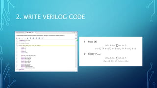
This document provides an overview of using Verilog and Xilinx Vivado to design and simulate a simple combinational circuit. It describes setting up Vivado, writing Verilog code for a full adder circuit, synthesizing the code, writing a testbench, running a simulation, and verifying the results in the waveform. The goal is to familiarize users with the typical workflow of a computer-aided design tool for digital circuits.