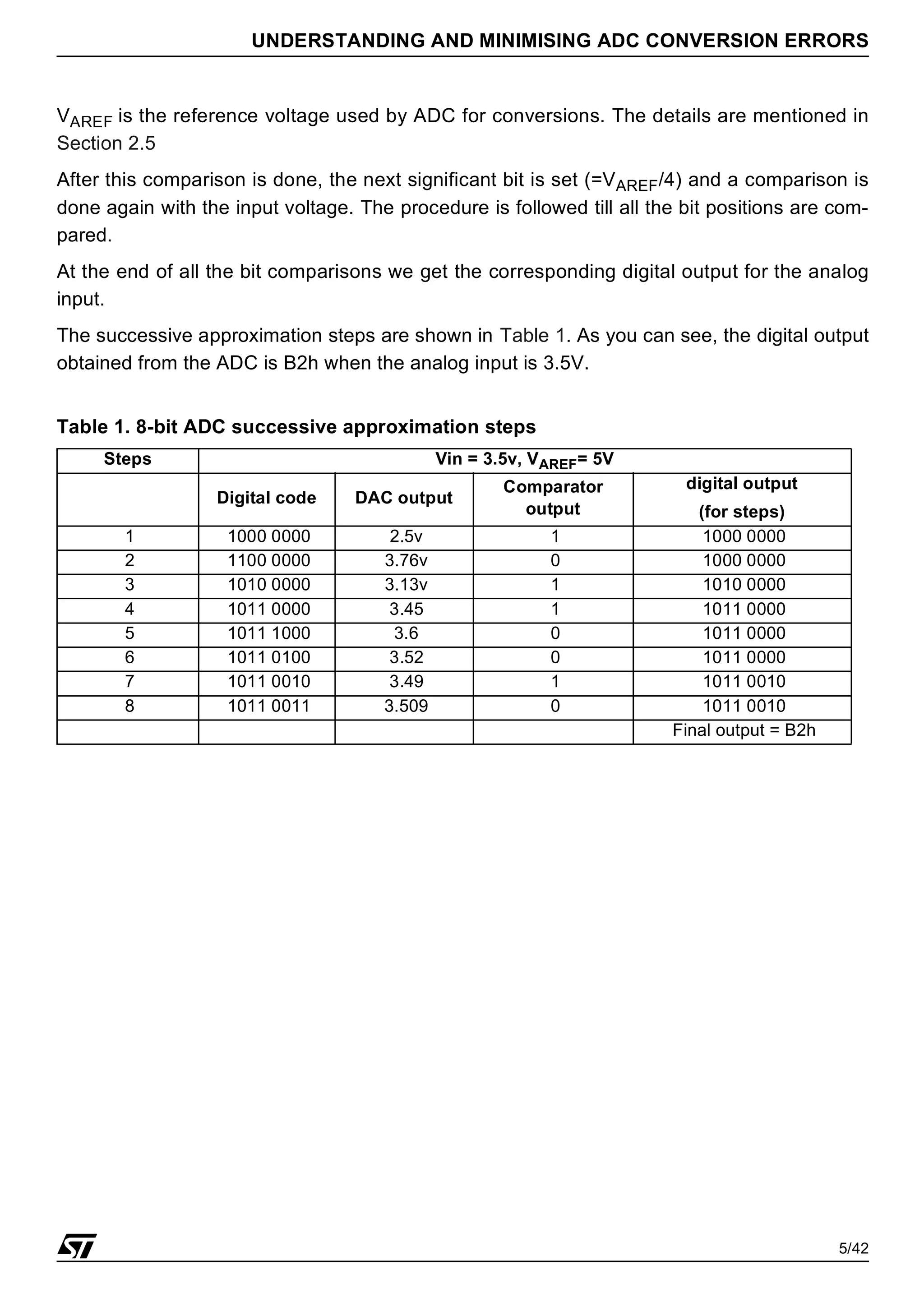
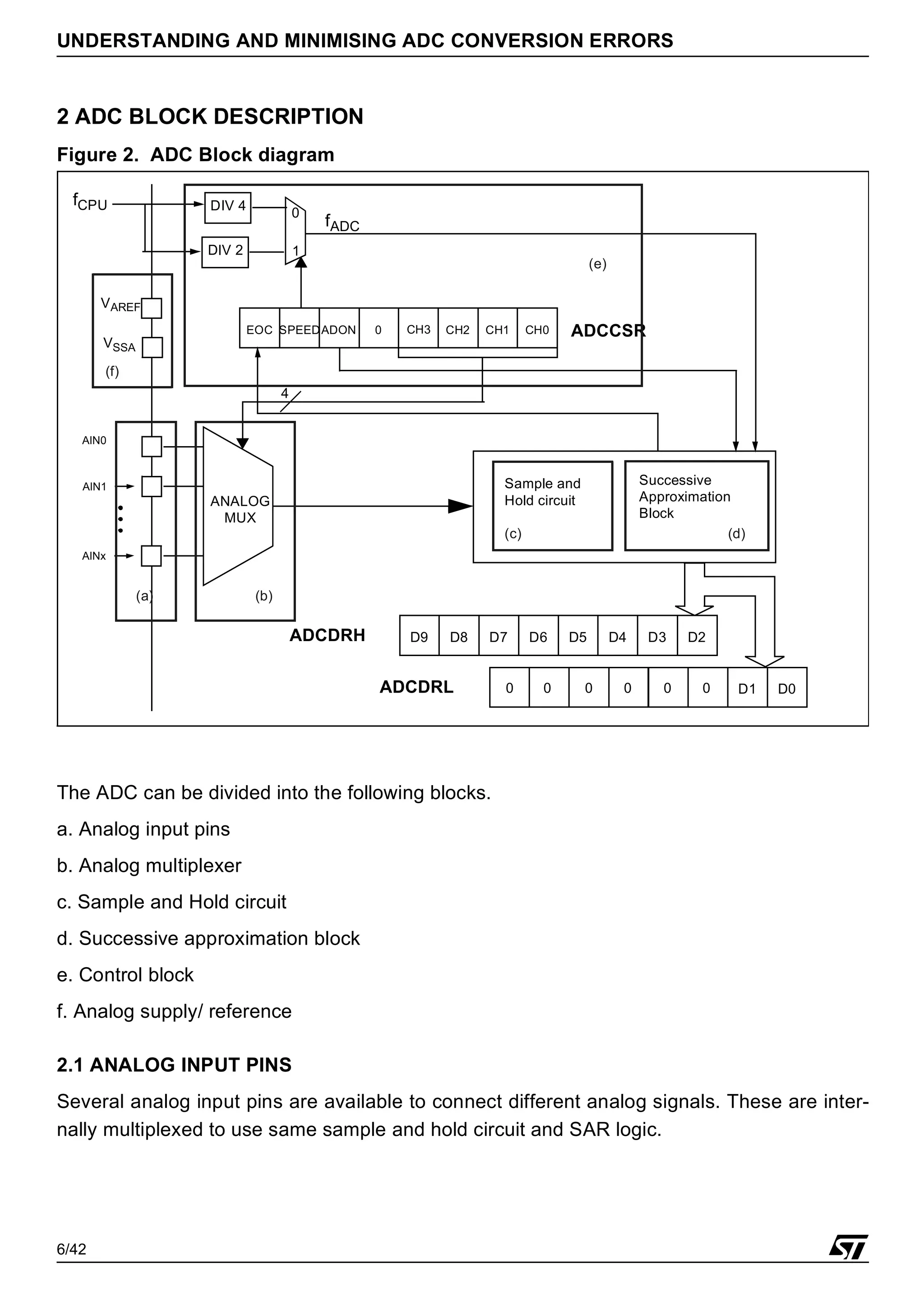
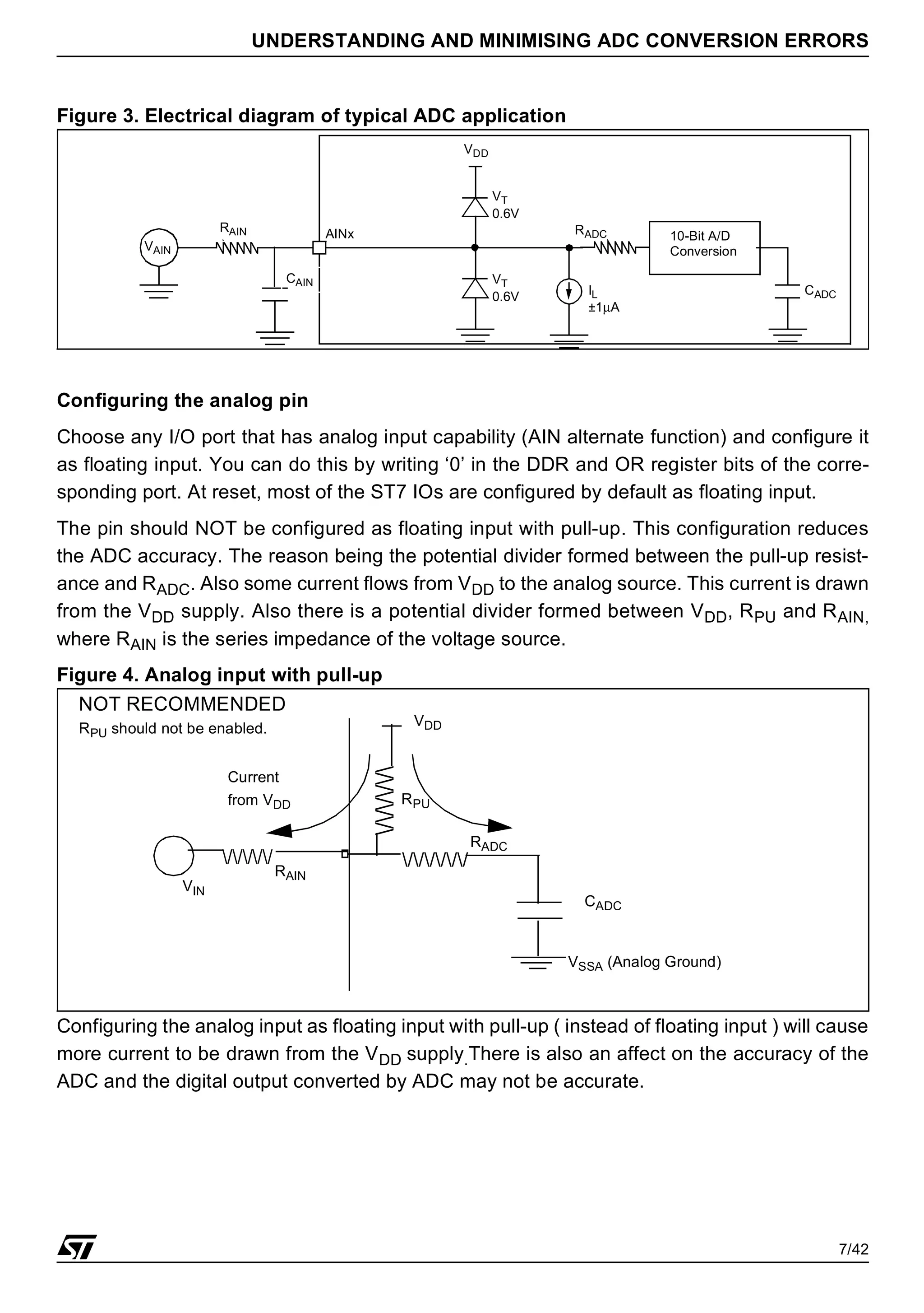
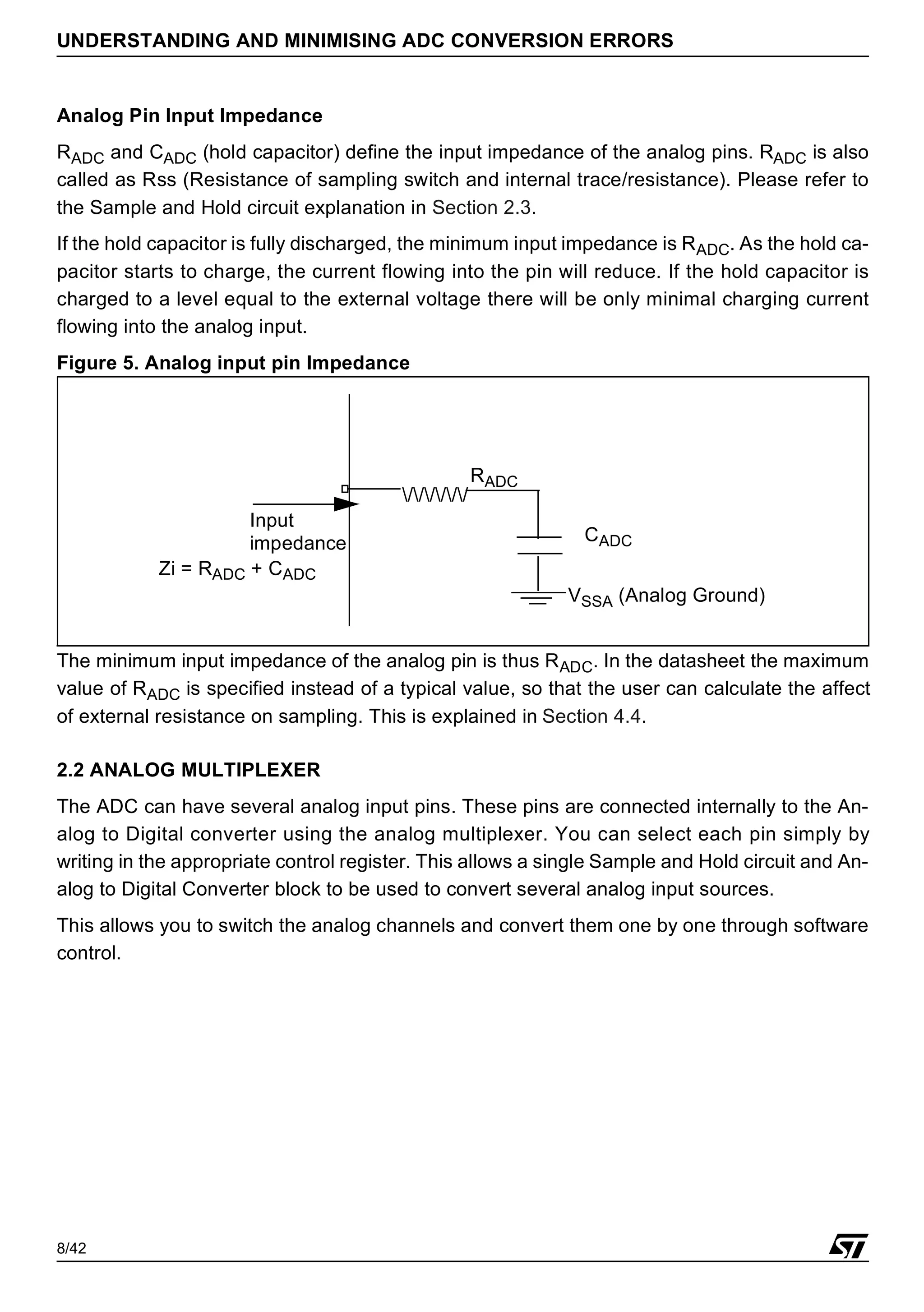
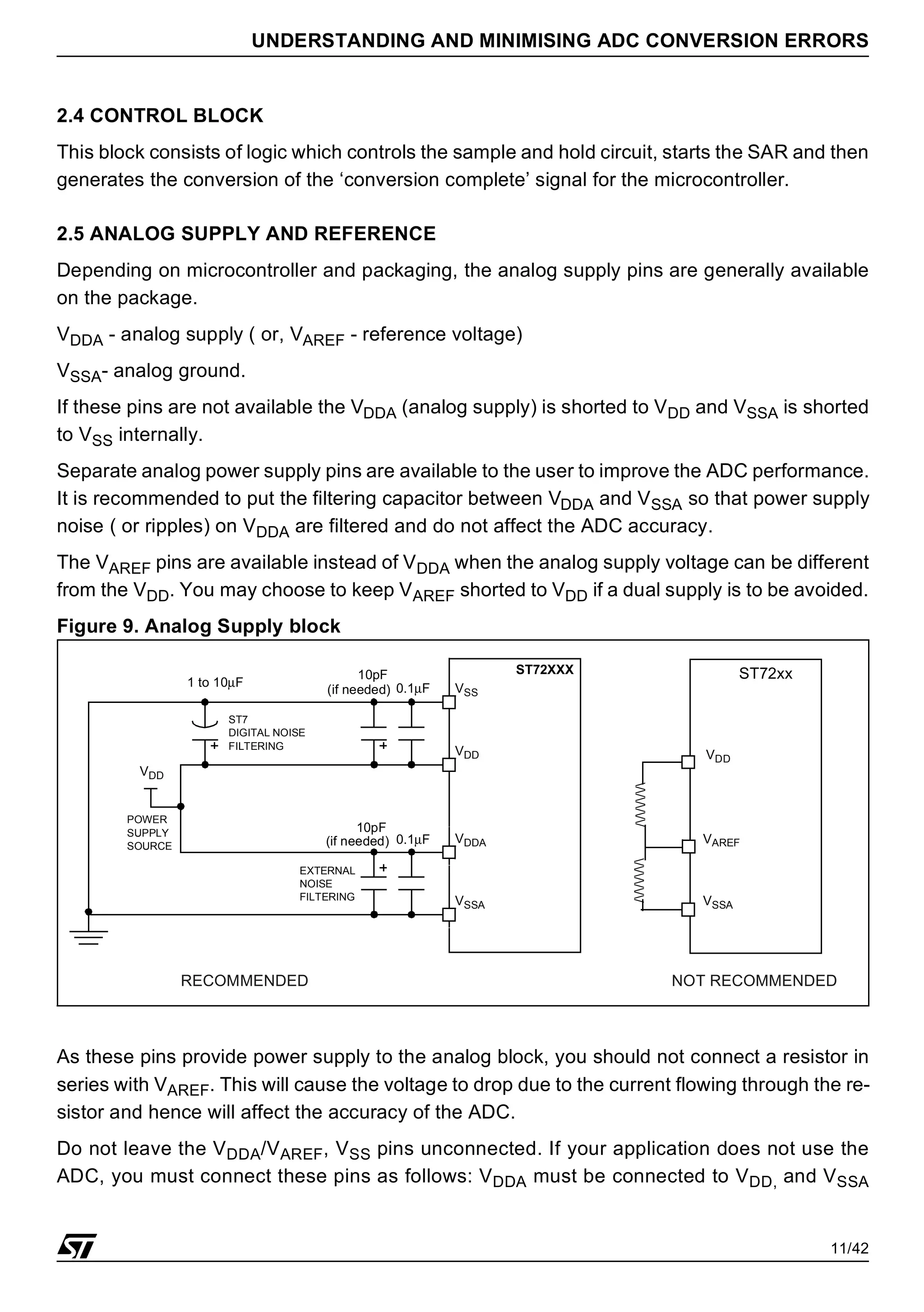
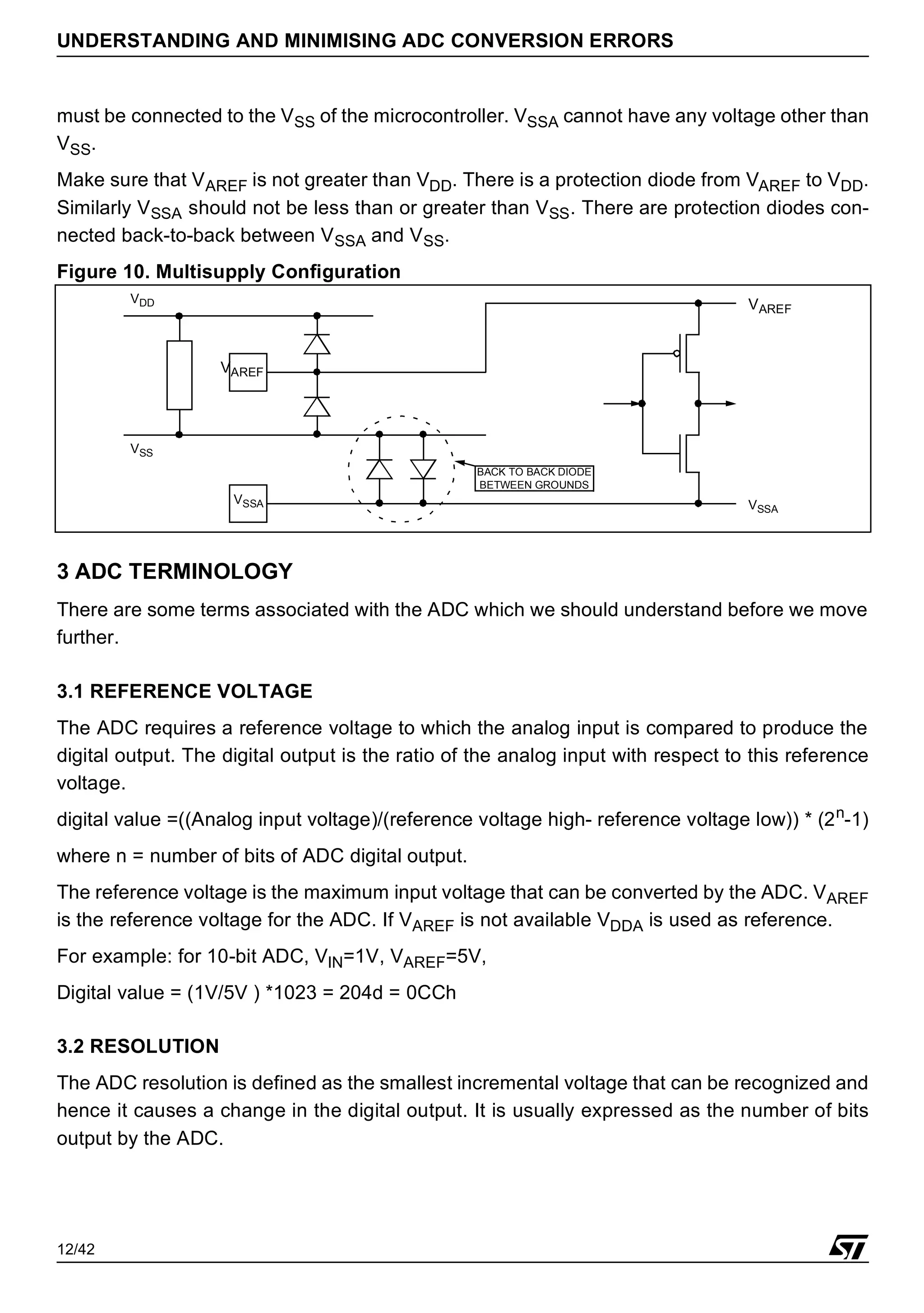
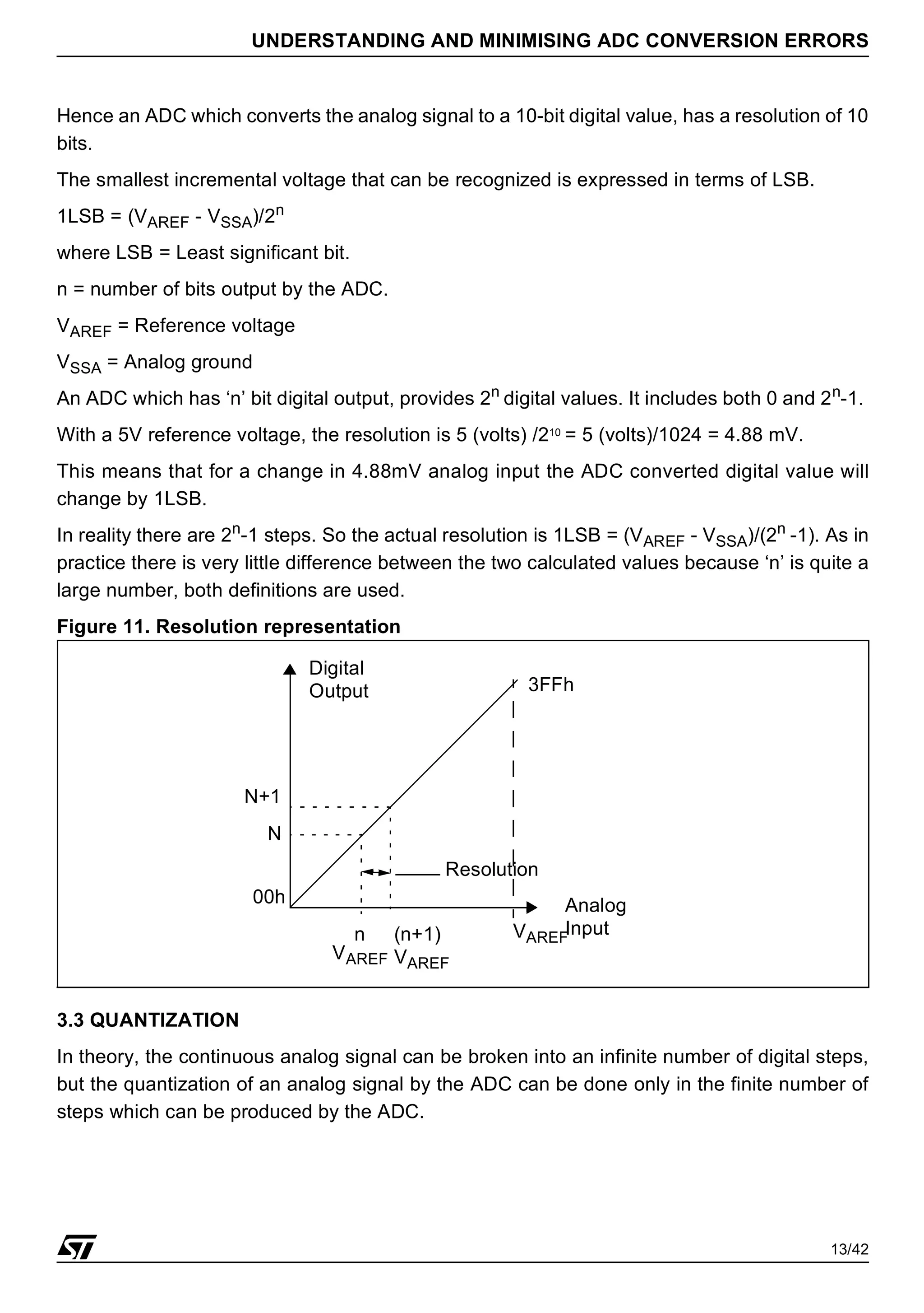
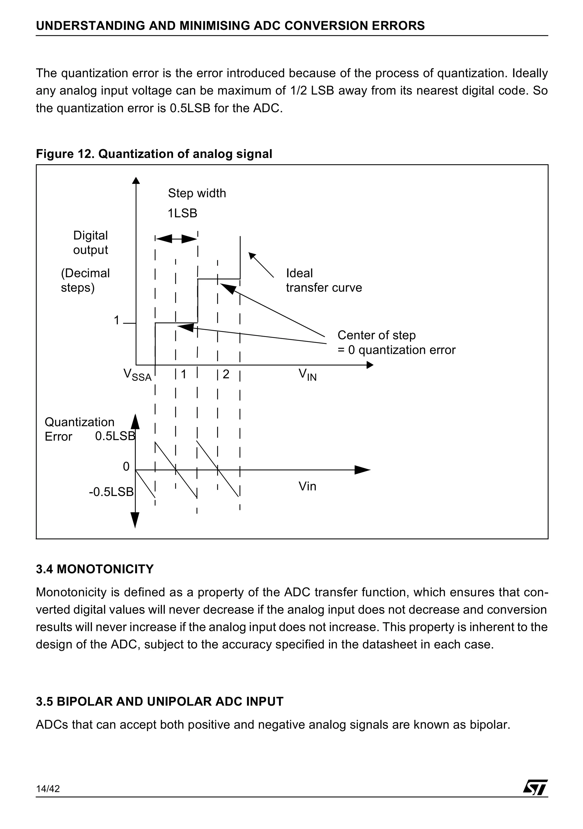
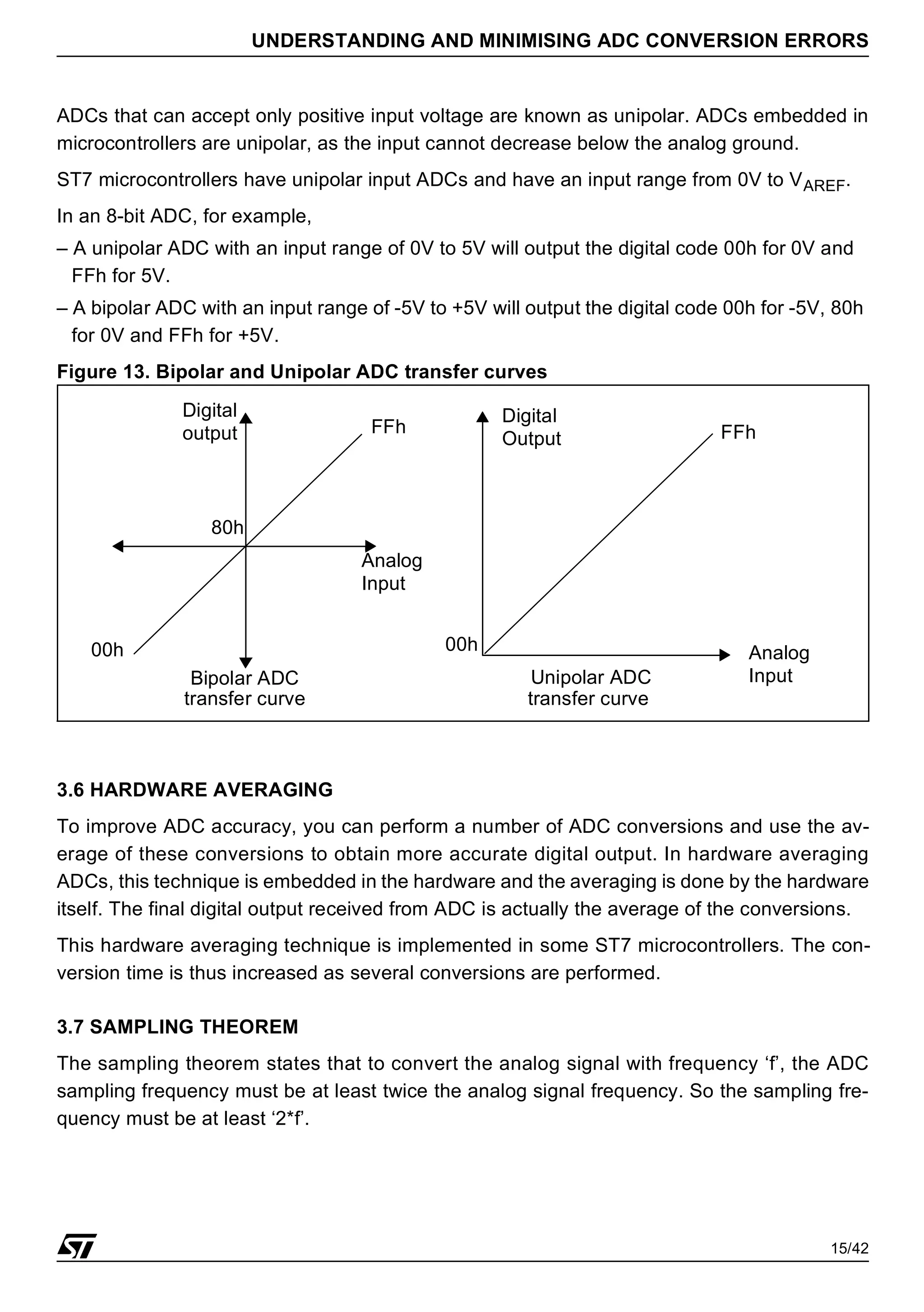
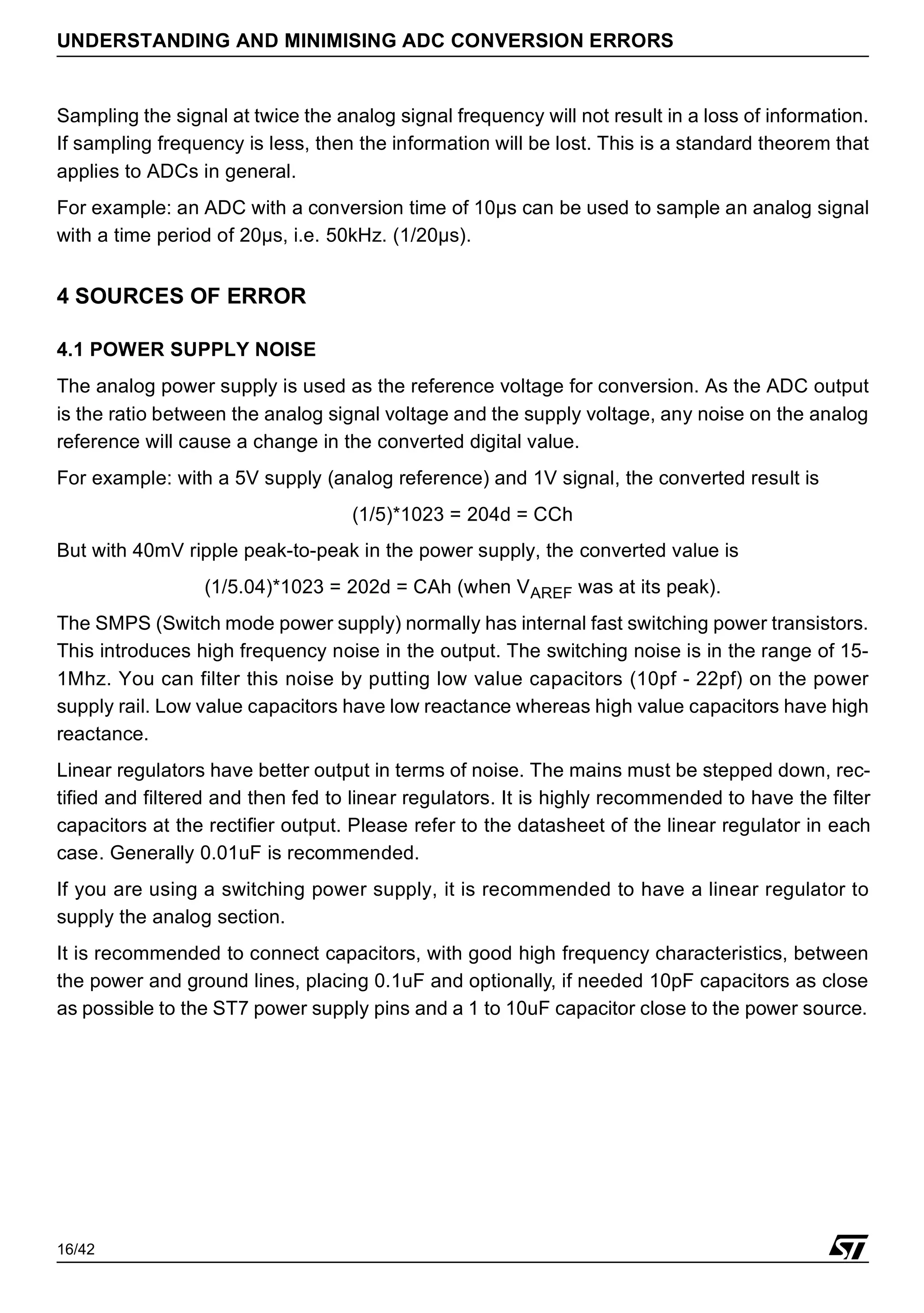
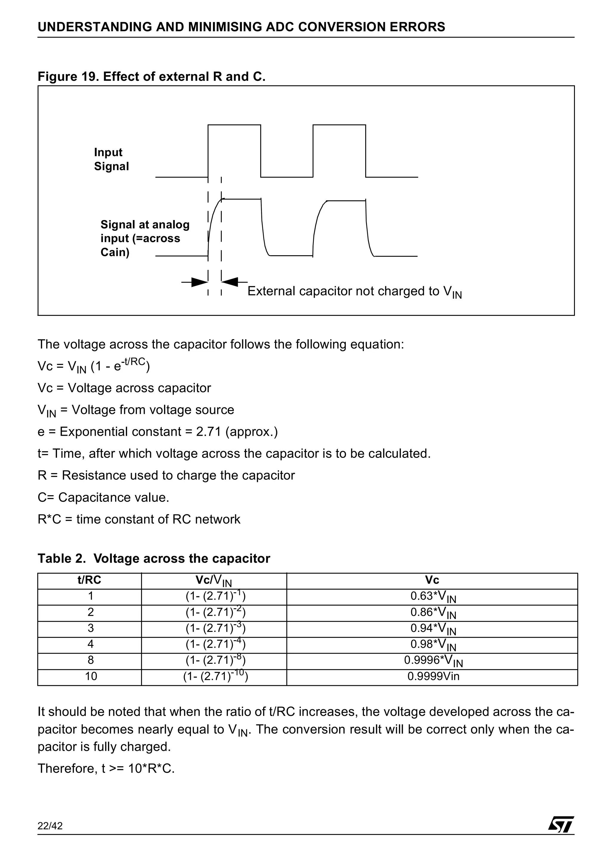
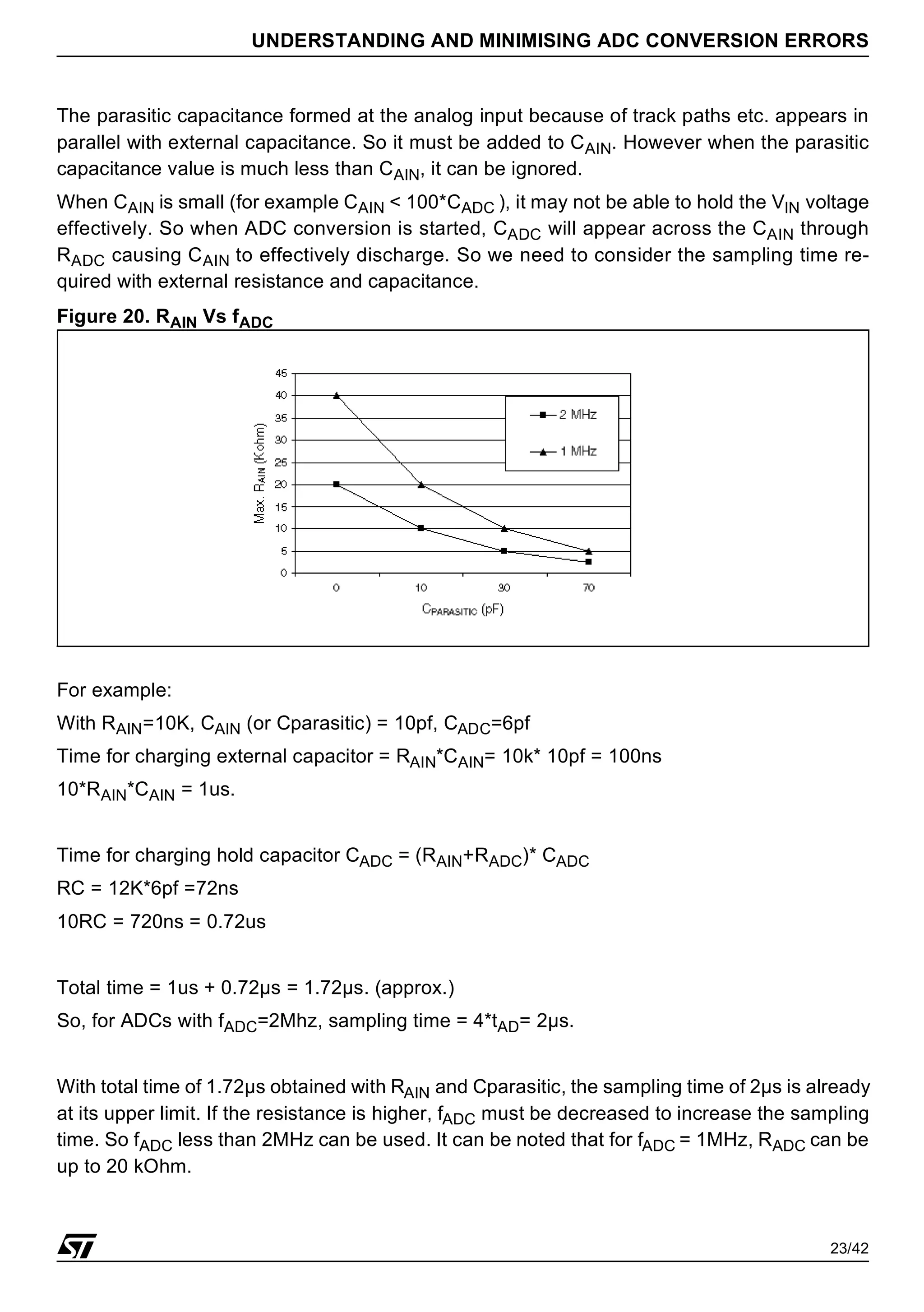
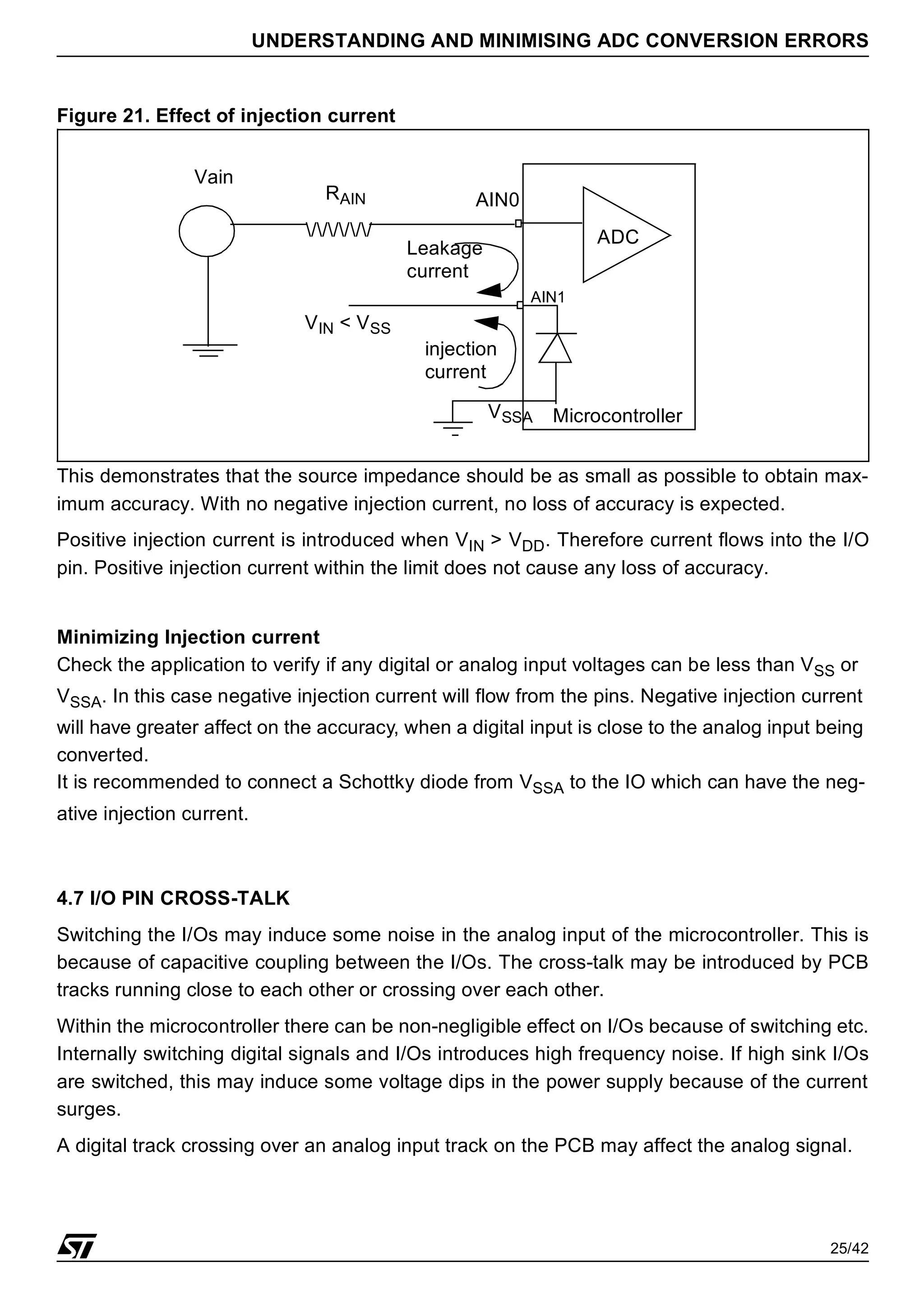
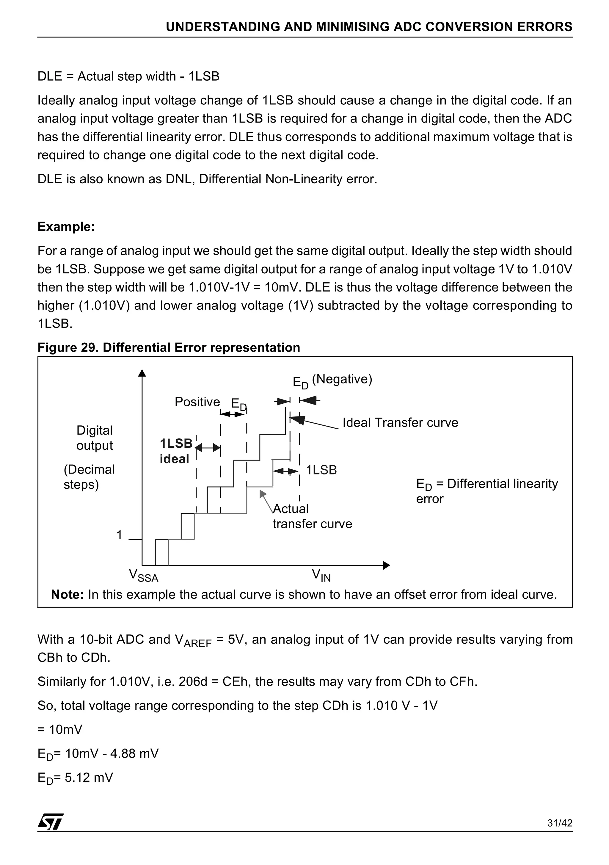
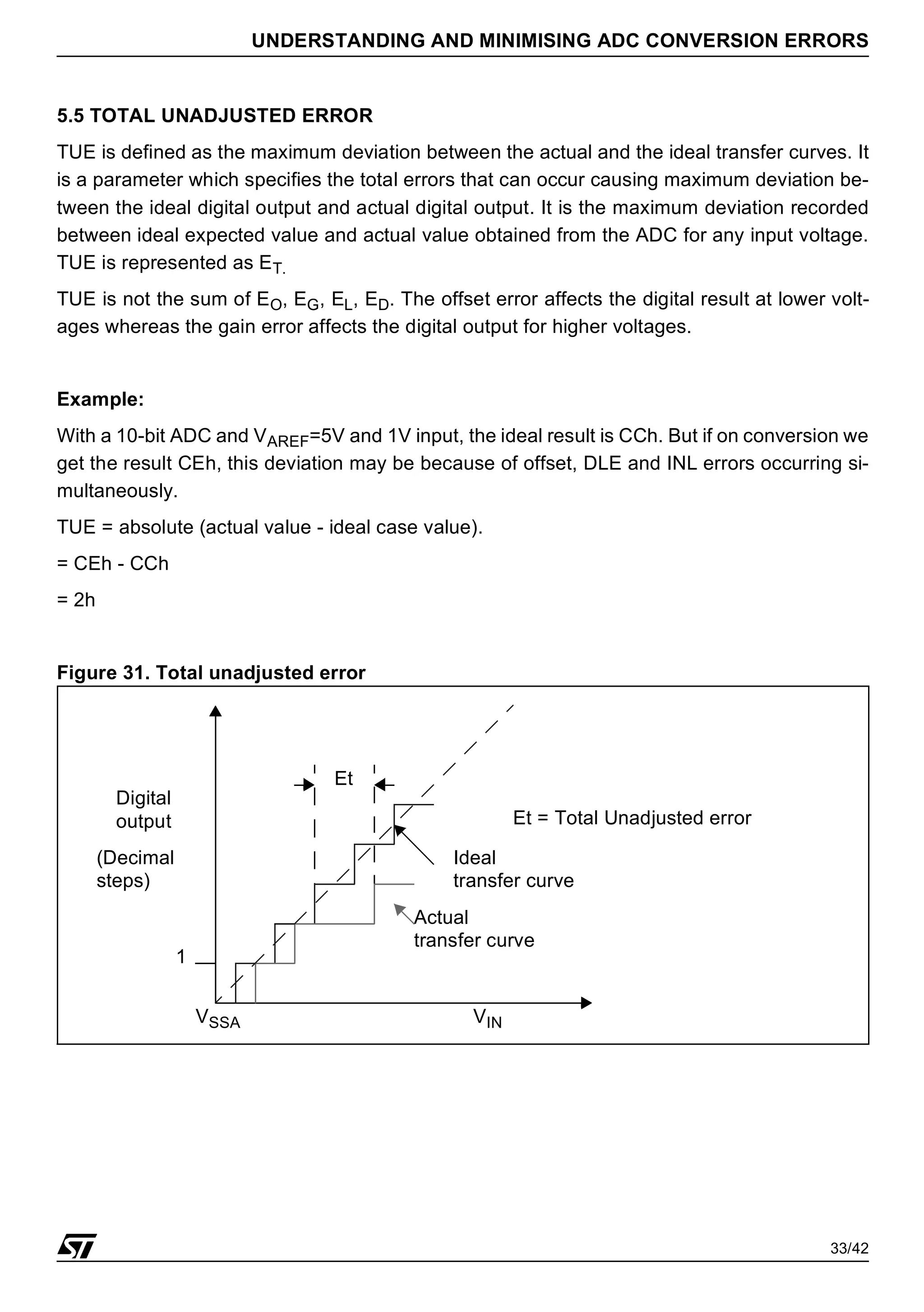
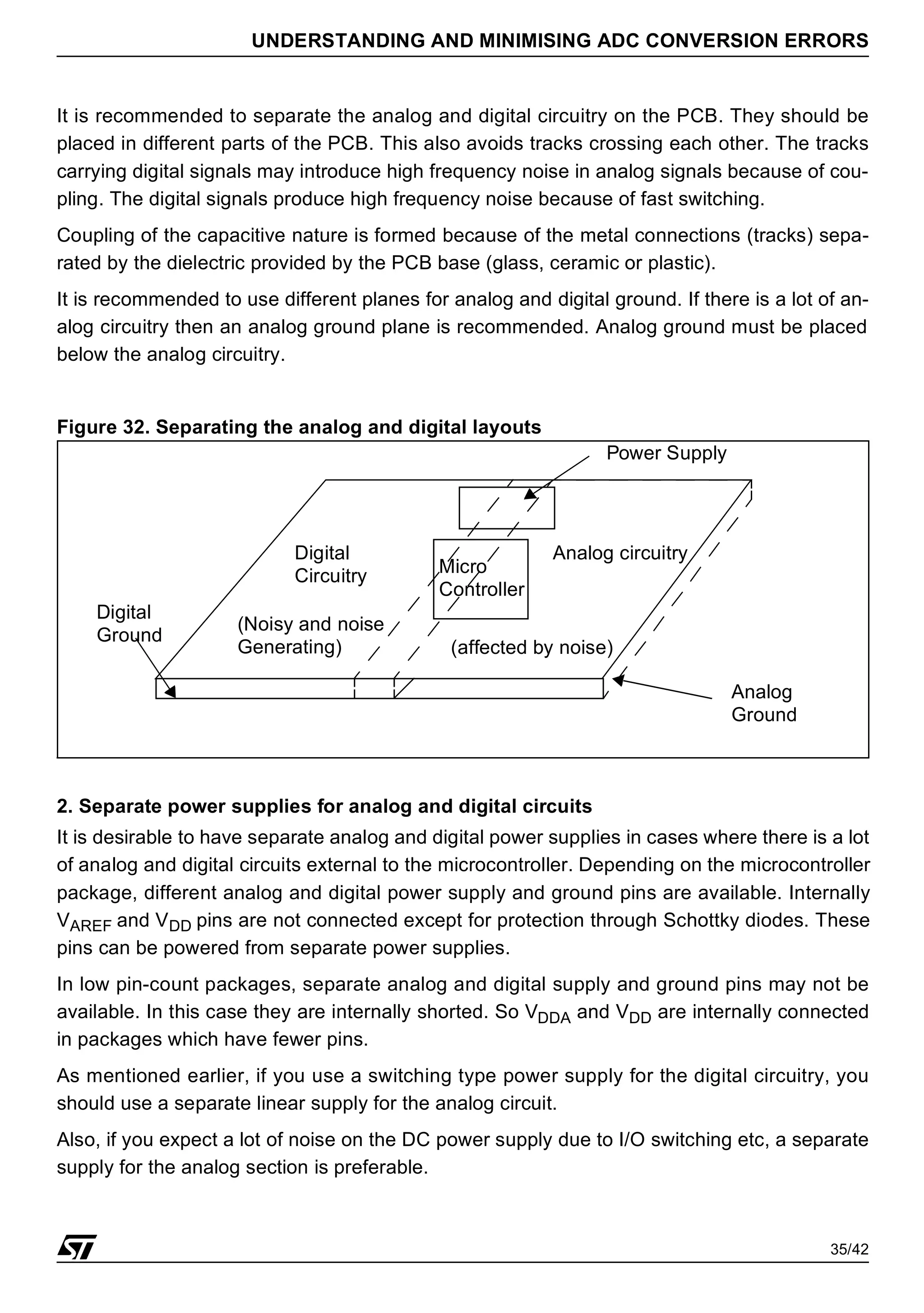
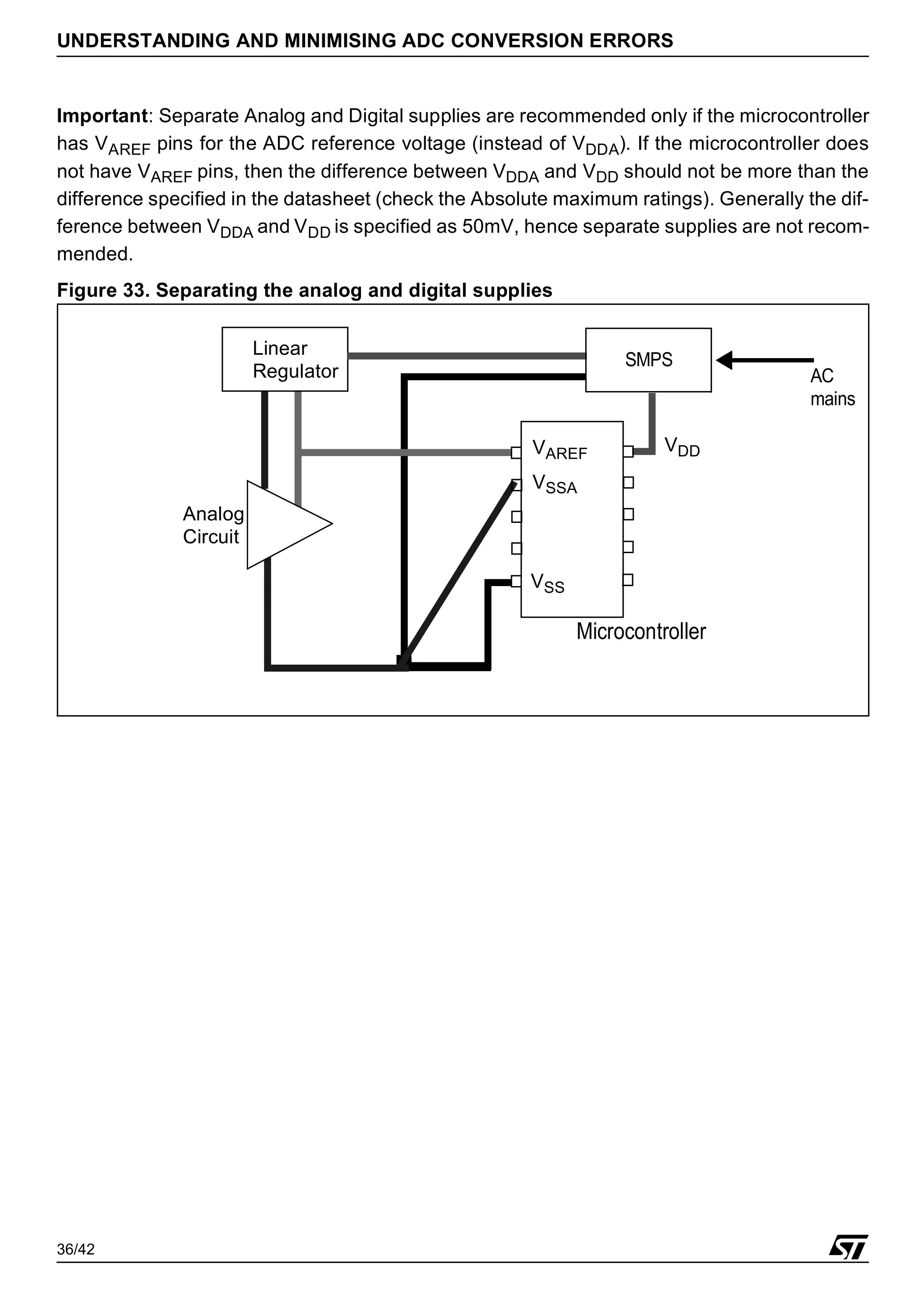
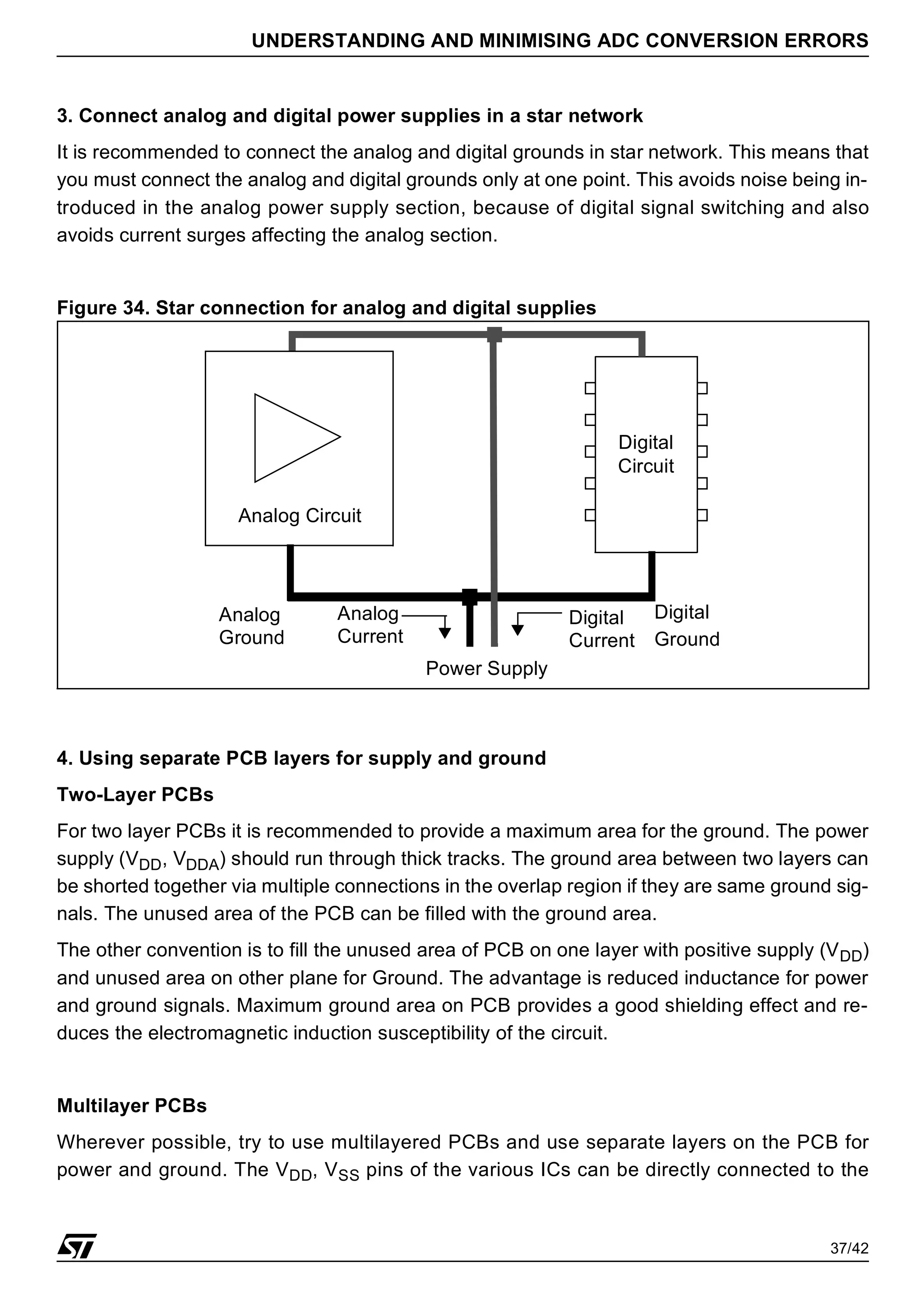
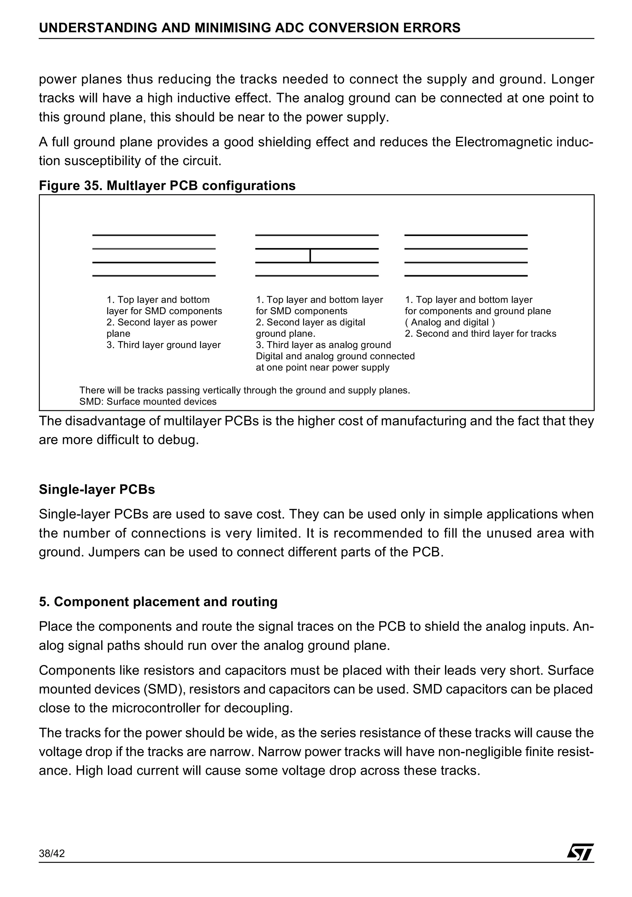
The document discusses understanding and minimizing errors in analog to digital conversion. It explains that the ADC converts analog signals to digital values but is subject to various errors from factors like noise, voltage sources, and PCB layout. It provides techniques to minimize errors, such as reducing noise, improving voltage regulation, and carefully designing PCB layout and analog signal paths.
![9/42
UNDERSTANDING AND MINIMISING ADC CONVERSION ERRORS
Figure 6. Analog multiplexer
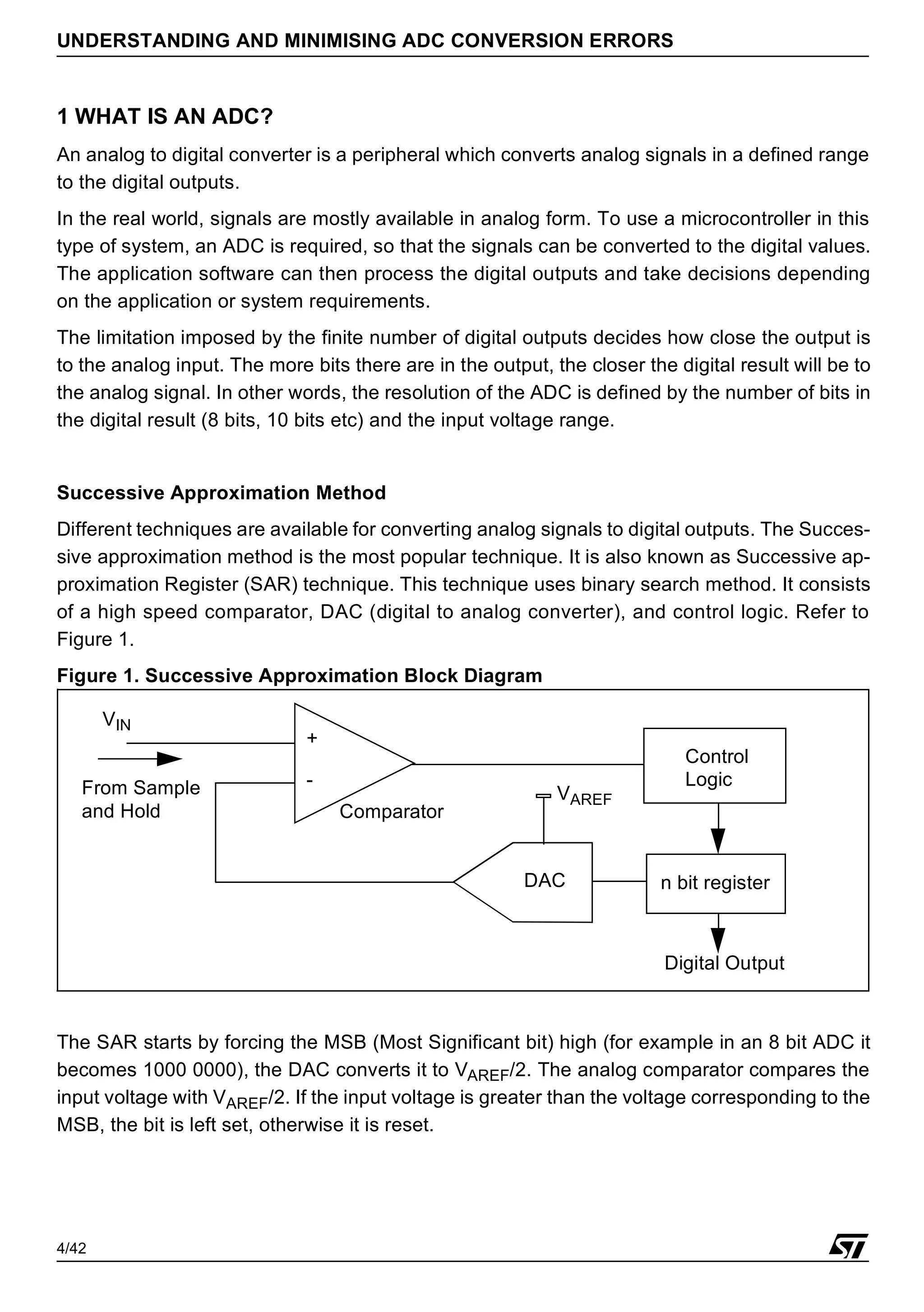
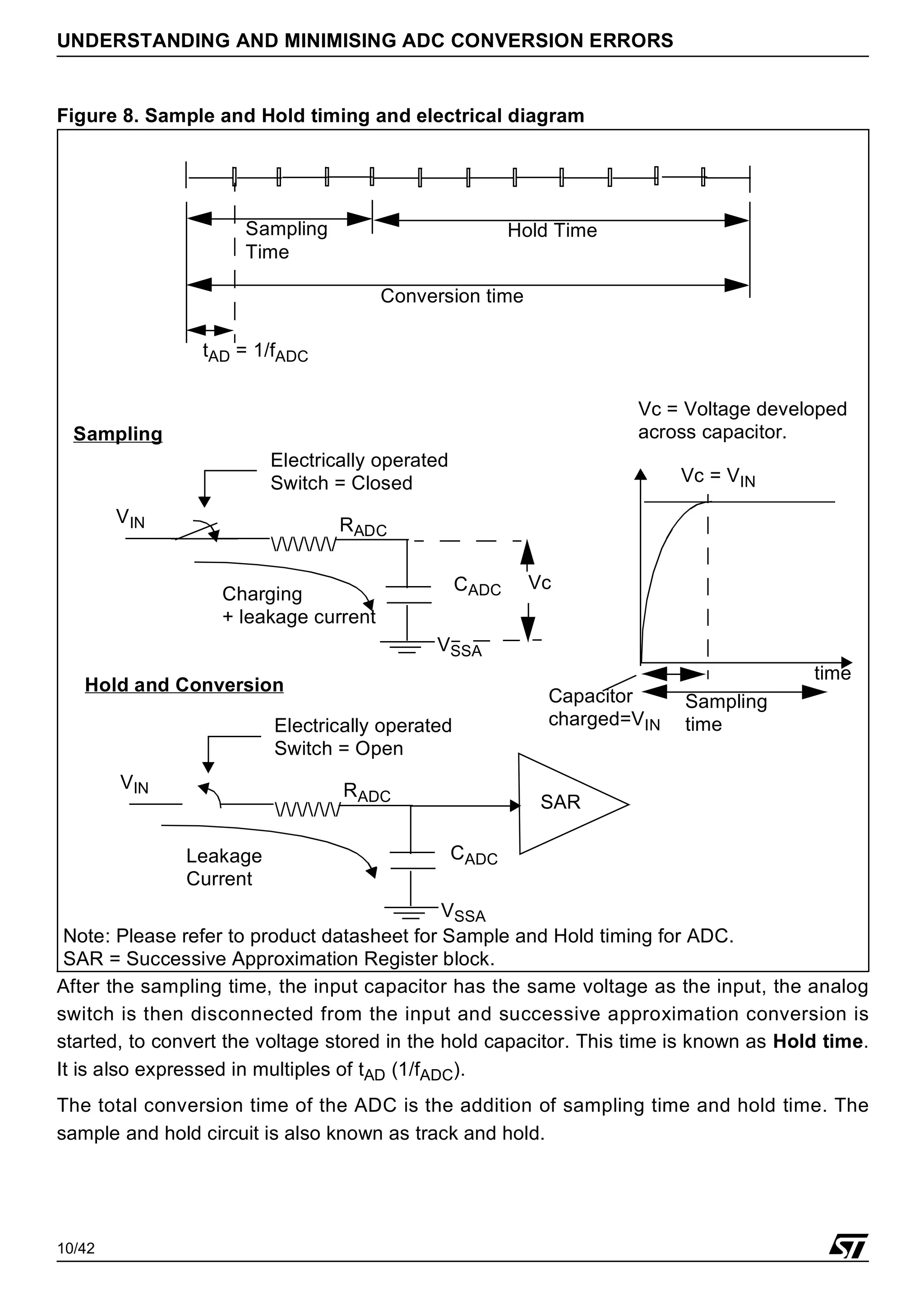
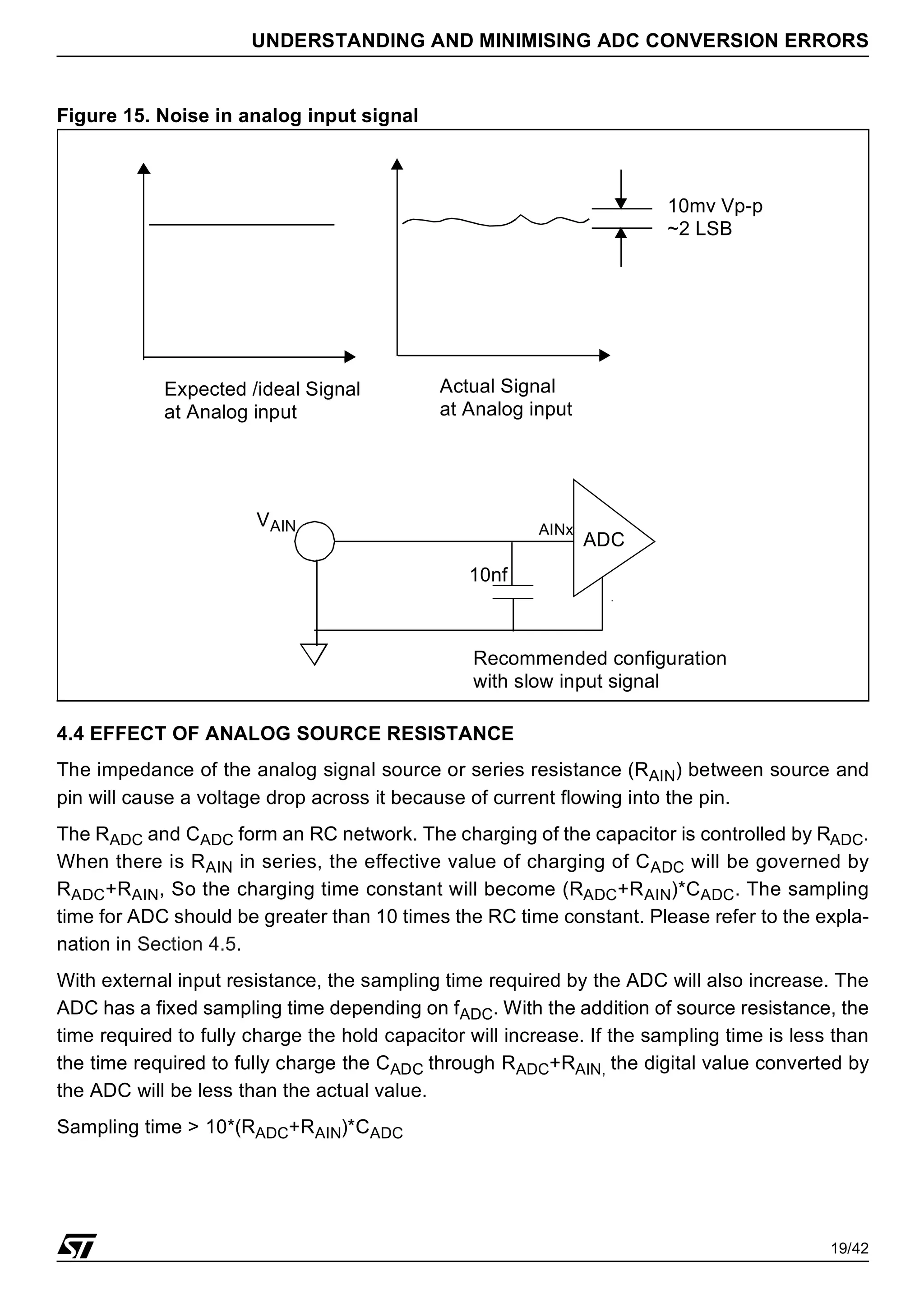
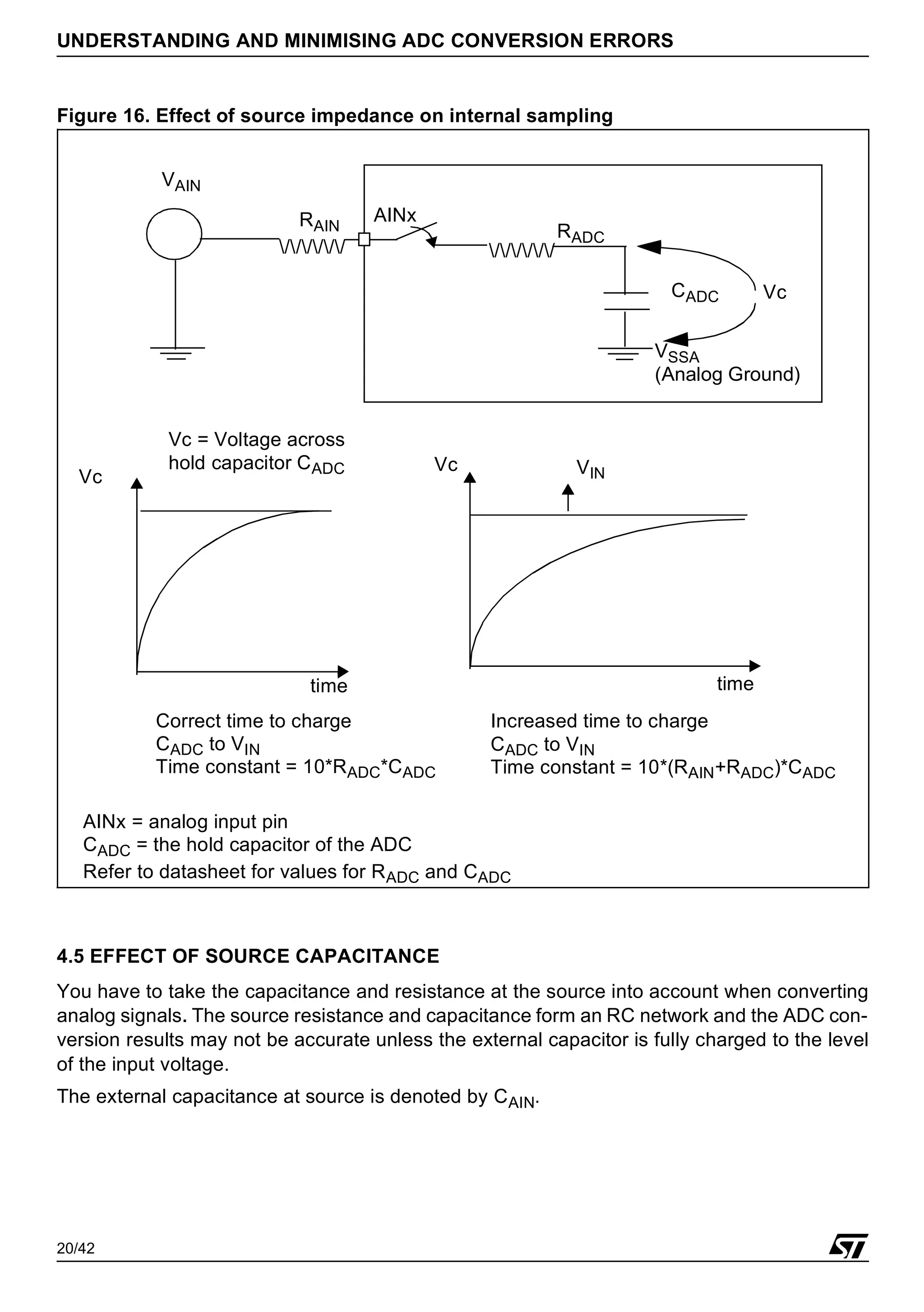
2.3 SAMPLE AND HOLD CIRCUIT
The sample and hold circuit samples the input signal and charges the internal hold capacitor
CADC to the voltage equal to VIN through RADC. The analog pin is then disconnected and the
voltage across the capacitor is then converted to digital code using successive approximation.
Figure 7. Sample and Hold circuit
The sample and hold circuit consists of an electrically operated analog switch, internal
charging resistance and hold capacitor.
As soon as the ADC conversion starts, the electrically operated switch is closed, connecting
the hold capacitor to the analog input through the internal ADC resistance RADC. This causes
a charging current to flow into the analog input and the capacitor starts to charge. The time the
switch remains closed is decided by the fADC. It is called sampling time. The sampling time is
generally indicated in the datasheet as a multiple of fADC clock periods.
Time period tAD = 1/fADC
CH[2:0] = 010
To Sample and Hold
AIN0
AIN1
AIN7
Circuit
Analog Input
Channels
Channel selection bits = 010 selects
AIN2
AIN2
//////
Electrically operated
switch
CADC
RADC
From Analog
Multiplexer
VSSA (Analog Ground)
VIN](https://image.slidesharecdn.com/cd00004444-understanding-and-minimising-adc-conversion-errors-stmicroelectronics-220111132945/75/Cd00004444-understanding-and-minimising-adc-conversion-errors-stmicroelectronics-9-2048.jpg)


![1. SIH2025-IDEA-Presentation-Format[1].pptx](https://cdn.slidesharecdn.com/ss_thumbnails/1-251204091914-b1bb69d5-thumbnail.jpg?width=640&height=640&fit=bounds)


