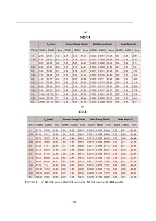
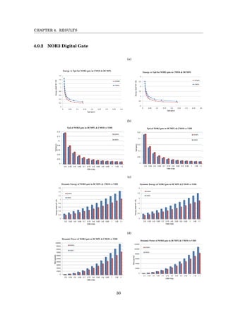
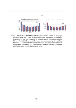
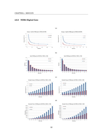
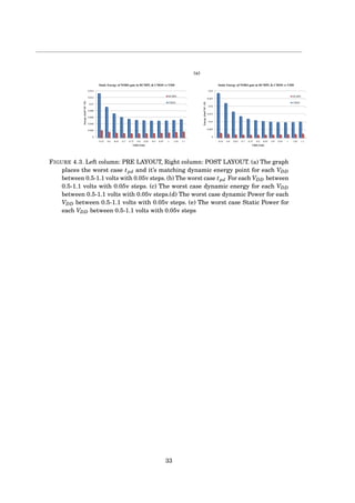
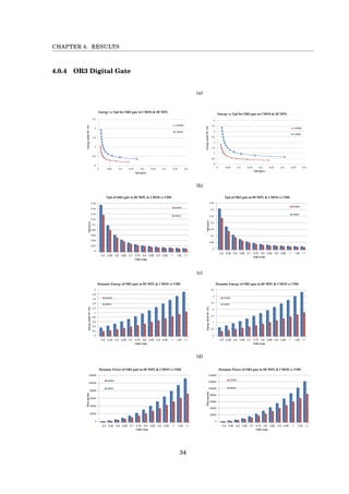
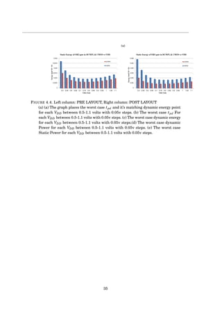
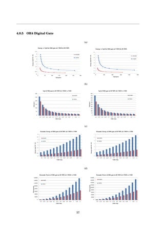
This document presents a project book on designing DCMPL logic circuits in a 28nm process technology. It was authored by Itamar Greenberg and Shay Rubinstein from the Department of Electrical Engineering at Bar Ilan University. The document includes an introduction to CMOS scaling challenges, a literature survey of logic families such as diode logic, RTL, TTL, NMOS, PMOS and CMOS. It describes the design, modeling, layout and simulation of various digital logic gates including NOR3, NOR4, OR3 and OR4 gates. Simulation results on propagation delay, energy consumption, voltage transfer curves and noise margins are presented and analyzed.

![CHAPTER
1
INTRODUCTION
F
or over four decades scientists have been scaling increasingly smaller devices trying to
maintain the "MOORE" law. This trend caused by unending demand for high performance
appliances such as laptops, cellphones, and "IOT"-internet of things. Another challenge
these days is dealing with growing competition between the chip design companies. No matter
how the future of the VLSI world will look like one steady rule will stay: It is impossible to
improve power consumption, performance, and area of the chip at the same time. Or in other
words: "there is no free lunch". In this chapter we describe the main issues that concern engineers
dealing with the CMOS unreliability problems in process and integrating IP’s for nanometer
technology. The intent of this chapter is not to give an in-depth description of the failure behind
the problems, but to provide the reader with the basic knowledge of CMOS reliability problems
and how they affect the performance at gate level circuit. First, sec 1.1 outlines how various
unreliability effects came into play in the course of history. Later sec 1.2 we will briefly explain
the mainstream unreliability effects such as spatial unreliability effects and time-dependent
unreliability effects.
1.1 History
The reliability of digital devices was first studied in the 1960’s, when complex integrated systems
were developed for the first time. The most famous conference which brought the physical unre-
liability problem to light was the first international reliability physics symposium (IRPS 1962,
Chicago).
During the 1970’s effects such as ionic contamination and corrosion were the most common causes
of circuit failure. During the 1980’s integrated reliability issues became visible. Further scaling
of the oxide thickness had increased the electrical field between the gate and the bulk, which
creates the hot carries injection phenomenons that eventually harm the gate performance.
Initially, arbitrary voltage stress resulted in an identical parameter shift for matched devices [5].
So at the beginning this kind of unreliability effects were considered as deterministic problems.
However, when oxide dielectrics reached the atomic- scale dimension, it resulted in the first
stochastic temporal unreliability effect. In the late 1980’s when the dimensions of the devices
1](https://image.slidesharecdn.com/9a1e0d8e-e59a-4d22-b9a1-bf4a38f20b86-161117162512/85/DCMPL_PROJECT_BOOK_SHAY_ITAMAR-7-320.jpg)
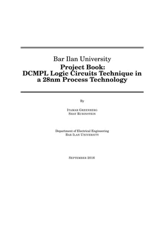
![CHAPTER 1. INTRODUCTION
Figure 1.1: CMOS parameters during scaling. Figure reproduced from [? ].
had scaled to the nanometeric realm, stochastic errors and variations at the atomic level became
apparent at device level and sensitive analog circuits were the first to suffer from process vari-
ability effects (Lakshmi Kumar et al. 1986; Pelgrom et al. 1989).
Device mismatch became a big issue (especially analog) designers had to deal with in order to
guarantee good accuracy and high yield.
2](https://image.slidesharecdn.com/9a1e0d8e-e59a-4d22-b9a1-bf4a38f20b86-161117162512/85/DCMPL_PROJECT_BOOK_SHAY_ITAMAR-8-320.jpg)
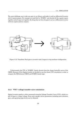
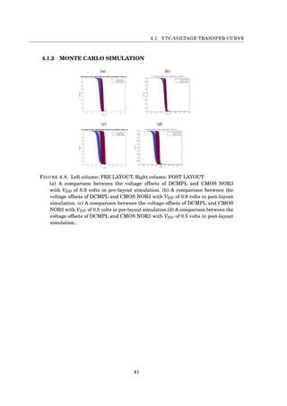
![2.1. LOGIC FAMILIES
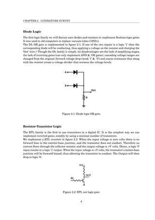
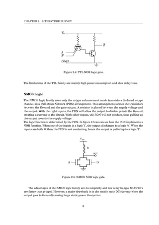
The same principles will apply for a NOR gate, as seen in figure 2.3. This time if any of the
input rises to ’1’ then the corresponding transistor will conduct, which will result in the output
discharging.
Figure 2.3: RTL NOR3 logic gate.
The obvious disadvantage of RTL is its high power dissipation when the transistor is switched
on (the power is dissipated mainly by the base resistors connected to logical "1" and by the
collector resistor). This requires that more current be supplied to and heat be removed from RTL
circuits [2].
Transistor-Transistor Logic
Invented in 1961, The TTL family uses transistors to implement the logic function and to amplify
the signal.
A TTL NAND gate is implemented in figure 2.4. When the two emitters of the input transistors
are connected to high voltage, then the emitter-base junction of the transistor is reverse biased,
that means the transistor is in reverse active mode. In reverse active mode, less magnitude
current flows in the opposite direction. This current reaches the base of the output transistor,
allowing it to conduct and pulling down the output voltage to zero. When any one of the input
terminal is low, the current through other branch flows out through this terminal. Now no current
reaches the base terminal of the output transistor, so output remains at high state [4].
5](https://image.slidesharecdn.com/9a1e0d8e-e59a-4d22-b9a1-bf4a38f20b86-161117162512/85/DCMPL_PROJECT_BOOK_SHAY_ITAMAR-11-320.jpg)
![2.1. LOGIC FAMILIES
The PMOS logic family is similar to NMOS, except it uses p-type transistors and places them
at the Pull-Up Network (PUN) and a resistor attached to Ground.
Pass Transistor Logic
Up until now we saw logic families with transistors connected to supply/Ground voltages at
one end. The PTL family uses transistors as switches to pass logic levels between nodes of a
circuit, without these transistors being connected to a supply voltage. This feature can reduce the
number of transistors used to implement a logic function by eliminating redundant transistors.
PTL comes extremely handy when producing complicated gates and memory cells like Multiplex-
ers, Flip-Flops and SRAM. Figure 2.6 shows a PTL Multiplexer using only two transistors. The
implementation is very simple to understand [3].
Figure 2.6: PTL MUX gate uses only two transistors
However, we notice that the NMOS transistors will pass a weak ’1’. To avoid that, we use a
transmission gate as seen in figure 2.7. The PMOS transistor passes a strong ’1’ and the NMOS
transistor passes a strong ’0’.
Figure 2.7: Transmission gate
7](https://image.slidesharecdn.com/9a1e0d8e-e59a-4d22-b9a1-bf4a38f20b86-161117162512/85/DCMPL_PROJECT_BOOK_SHAY_ITAMAR-13-320.jpg)
![CHAPTER 2. LITERATURE SURVEY
Complimentary MOS Logic
The CMOS family is a combination between the NMOS and PMOS families. The PDN consists of
n-type transistors and the PUN consists of p-type transistors. In that case, both the PDN and the
PUN have to implement the logic function.
Figure 2.8 shows the design of a NAND and NOR logic gates. We can see the relation between
the PDN and the PUN in a given CMOS gate. If the PDN has a parallel formation then the PUN
has a serial formation, and vise-versa.
Figure 2.8: CMOS NAND and NOR logic gates.
The CMOS design has managed to achieve great improvements in numerous parameters,
reaching characteristics of almost an ideal logic family. [1]
First, the static power dissipation decreases dramatically. Unlike the NMOS/PMOS logic
families, there will never be a straight path between the supply voltage and the Ground. This is a
result of the relation between the PDN and the PUN which are always complimentary, meaning
that when one is conducting the other is not. The static power dissipation is caused only by
leakage currents. These currents are more significant as the device is scaled.
Secondly, the propagation delay is rather short for both networks, though the NMOS is faster
than PMOS. In order to make both networks equal in respect to propagation delay time we use
wider p-type transistors in the PUN. The ratio between the widths of the n-type and the p-type
transistors is represented by "Œ ≤". The Œ ≤ parameter depends on the technology we are using.
Third, the rise and fall times are controlled by the sizing of the transistors. Last is the noise
margin. Ideally we want a noise margin of 50%. the supply voltage. The CMOS noise margin is
reaching values close to the ideal.
8](https://image.slidesharecdn.com/9a1e0d8e-e59a-4d22-b9a1-bf4a38f20b86-161117162512/85/DCMPL_PROJECT_BOOK_SHAY_ITAMAR-14-320.jpg)
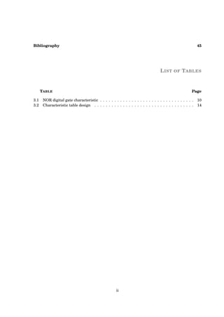
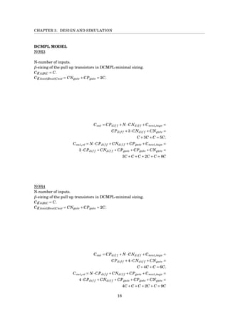
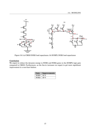
![3.2. MODELING
3.2 Modeling
In this chapter we aim to develop a mathematical model that anticipates the tpd and Energy of
the DCMPL logic gate for any given gate capacitance.
Power Consumption
Power Consumption of any circuit is divided into the following categories:
• Dynamic power ∼ Cload · vdd2
• static power ∼ Istatic · vdd
• short circuit power ∼ Tsc · Ipeek · vdd · f
We modeled the load capacitance which is critical for predicting the dynamic power when charging
the output of the gate. We ignore the voltage supply effect because the simulation uses each time
the same VDD . In order to find Cload we have to find all capacitance which connect directly to
wire OUT and OUTnot in both design.
In the CMOS design figure [a] the ’OUT’ wire connect to three Cdif f of the NMOS transistors,
one Cdif f of the PMOS transistor multiply by β, and the capacitance gate of the next stage.
In the DCMPL design figure [b] the ’OUT’ wire connect to three Cdif f of the NMOS transistors,
one Cdif f of the PMOS transistor, and the capacitance gate of the next stage.
more over the OUTnot wire connect to three Cdif f of the PMOS transistors, one Cdif f of the
NMOS transistor, and the capacitance gate of INPUTnot of the next stage.
CMOS MODEL:
NOR3
N-number of inputs.
β-sizing of the pull up transistors in CMOS.
CgA|B|C = β·C +C = 4.9C.
Cout = β·CPdif f + N ·CNdif f +Cnexts tage =
3.9·CPdif f +3·CNdif f +CPgate +CNgate =
3.9C +3C +3.9C + c = 11.8C
NOR4
N-number of inputs.
β-sizing of the pull up transistors in CMOS.
CgA|B|C = β·C +C = 6.2C.
Cout = β·CPdif f + N ·CNdif f +Cnexts tage =
5.2·CPdif f +4·CNdif f +CPgate +CNgate =
5.2C +3C +5.2C + c = 14.4C
15](https://image.slidesharecdn.com/9a1e0d8e-e59a-4d22-b9a1-bf4a38f20b86-161117162512/85/DCMPL_PROJECT_BOOK_SHAY_ITAMAR-21-320.jpg)
![CHAPTER 3. DESIGN AND SIMULATION
Tpd - Elmore Delay
We use the Elmore-Delay in order to model the delay of the gate through the worst case vector by
charging and discharging the output.
In each one of the design we find the total capacitance and resistance go through transistors from
input to output.
At last we modeled how the trend line of tpd vs VDD should look like.
First we find who is the longest vector[fig3.7]. The vector who has to pass more capacitance on
the way is tplh(out) form input A.
Second we use Elmore-Delay model find how many capacitance and resistance on the critical
path so the general equation for unknown β and inputs is:
Third we know from VLSI course (assuming Cdif f const) that:
We subtitute R,C,S,β in the equation above and find that: tpd graph ∼ const· 1
V dd
In Summery we expect the tpd vs VDD will act like 1
x graph.
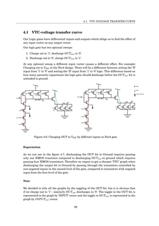
Figure 3.7: Charging OUT to VDD by different inputs in Nor4 gate
18](https://image.slidesharecdn.com/9a1e0d8e-e59a-4d22-b9a1-bf4a38f20b86-161117162512/85/DCMPL_PROJECT_BOOK_SHAY_ITAMAR-24-320.jpg)
![3.3. LAYOUT
3.3 Layout
The layout stage is where we simulate the physical layers of our digital gate.
This is an importent stage since all the properties of our gate derive from it.
Due to the secrecy of the 28 nm proecess we can not show any photos of our layout, however we
will discuss some principles and challenges we encountered during the project as can be seen in
figure 3.8.
The first challenge was the limitation on breaking the polysilicon. furthermore the gap between
polysilicon layers must be constnt [1].
Secondly, minimizing the distance between diffusion layer is limited due to several design rules[2].
third, metal thickness often needs to increase significantly[3].
Figure 3.8: Layout Challenges in 28 nm
19](https://image.slidesharecdn.com/9a1e0d8e-e59a-4d22-b9a1-bf4a38f20b86-161117162512/85/DCMPL_PROJECT_BOOK_SHAY_ITAMAR-25-320.jpg)
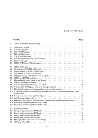
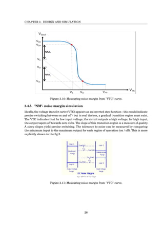
![CHAPTER 3. DESIGN AND SIMULATION
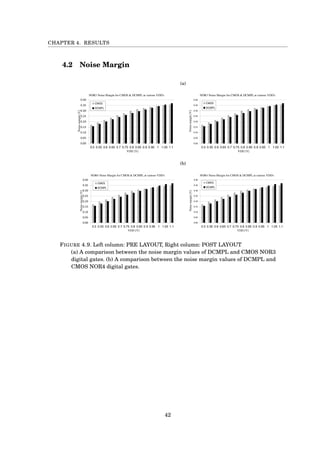
3.4.3 "SNM"- Static Noise Margin
The "SNM" analysis is taken from volatile memory cells such as SRAM memory.
We connected two gates as a ring oscillator of two inverters and checked what is the maximum
noise we can add to the input while still keeping a stable data in the cell.
In order to measure the SNM we used transformation circuits to rotate the VTC graph by 45◦
.
Then we ran a DC sweep from -VDD /sqrt(2) to VDD /sqrt(2) on V uaxis and found what is the
maximum diagonal of the square in the right and left side.
And finely, the minimum of the two diagonals will give us the "SNM" measurement.
(a) (b) (c)
(d) (e)
(f)
FIGURE 3.14. (a) A Ring oscillator configuration help to indicate what is max limit of
noise keep the system stable. Figure reproduced from [? ]. (b) Design of the first
transformation function that flip "Y" axis by 45◦
. Figure reproduced from [? ]. (c)
Design of the second transformation function that flip "X" axis by 45◦
.(d) The ideal
of the"snm" simulation is to find the max square in the overlapping area between
two original "VTC" curves.Figure reproduced from [? ]. (e) After we process two
max square from tow different overlapping area we compare between them and
take the minimal square for worst case scenario.Figure reproduced from [? ]. (f)
Summarizing all steps to find static noise margin in any system
24](https://image.slidesharecdn.com/9a1e0d8e-e59a-4d22-b9a1-bf4a38f20b86-161117162512/85/DCMPL_PROJECT_BOOK_SHAY_ITAMAR-30-320.jpg)
![BIBLIOGRAPHY
[1] R. J. BAKER, CMOS: circuit design, layout, and simulation (Second ed.), Wiley-IEEE,
2008.
[2] IBM, Transistor Component Circuits, IBM.
[3] C. F. H. JAUME SEGURA, CMOS electronics: how it works, how it fails, Wiley-IEEE,
2004.
[4] W. R. B. JR., MECL System Design Handbook 2nd ed., Motorola Semiconductor Prod-
ucts Inc. vi., 1972.
[5] B. SYKES, Why test bonds?, Global SMT & Packaging magazine, (2010).
45](https://image.slidesharecdn.com/9a1e0d8e-e59a-4d22-b9a1-bf4a38f20b86-161117162512/85/DCMPL_PROJECT_BOOK_SHAY_ITAMAR-51-320.jpg)