This Photo byUnknown author is licensed under CC BY-SA.
Course objectives:
Operation of Semiconductor diode,
Zener diode and Special purpose
diodes and their applications.
Biasing circuits for transistor (BJT)
as an amplifier.
Study of linear Op-amps and its
applications.
Logic circuits and their optimization.
Principles of Transducers and
Communication.
3.
Module-1 (8 hoursof pedagogy)
Semiconductor Diodes: Introduction, PN Junction diode, Characteristics and
Parameters, Diode Approximations, DC Load Line analysis.
Diode Applications: Introduction, Half Wave Rectification, Full Wave
Rectification, Full Wave Rectifier Power Supply: Capacitor Filter Circuit, RC π
Filter
Zener Diodes: Junction Breakdown, Circuit Symbol and Package,
Characteristics and Parameters, Equivalent Circuit, Zener Diode Voltage
Regulator.
Module-2 (8 hours of pedagogy)
Bipolar Junction Transistors: Introduction BJT Voltages & Currents, BJT
Amplification, Common Base Characteristics, Common Emitter Characteristics,
Common Collector Characteristics, BJT Biasing: Introduction, DC Load line
and Bias point.
Field Effect Transistor: Junction Field Effect Transistor, JFET Characteristics,
MOSFETs: Enhancement MOSFETs, Depletion Enhancement MOSFET.
Module-3 (8 hours of pedagogy)
Operational Amplifiers: Introduction, The Operational Amplifier, Block
Diagram Representation of Typical Op-Amp, Schematic Symbol, Op-Amp
parameters - Gain, input resistance, Output resistance, CMRR, Slew rate,
Bandwidth, input offset voltage, Input bias Current and Input offset Current, The
Ideal Op-Amp , Equivalent Circuit of Op-Amp, Open Loop Op-Amp
configurations, Differential Amplifier, Inverting & Non Inverting Amplifier
Op-Amp Applications: Inverting Configuration, Non-Inverting Configuration,
Differential Configuration, Voltage Follower, Integrator, Differentiator
4.
Module-4 (8 hoursof pedagogy)
Boolean Algebra and Logic Circuits: Binary numbers,
Number Base Conversion, octal & Hexa Decimal
Numbers, Complements, Basic definitions, Axiomatic
Definition of Boolean Algebra, Basic Theorems and
Properties of Boolean Algebra, Boolean Functions,
Canonical and Standard Forms, Other Logic Operations,
Digital Logic Gates.
Combinational logic: Introduction, Design procedure,
Adders- Half adder, Full adder
Module-5 (8 hours of pedagogy)
Introduction to Transducers: Introduction, Resistive
Transducers, Inductive Transducers, Capacitive
Transducers, Thermal transducers, Optoelectronic
transducer, and Piezoelectric transducers
Communications: Introduction to communication,
Communication System, Modulation
5.
Books
Electronic Devices andCircuits, David A
Bell, 5th Edition, Oxford, 2016
Op-amps and Linear Integrated Circuits,
Ramakanth A Gayakwad, Pearson Education,
4th Edition
Digital Logic and Computer Design, M.
Morris Mano, PHI Learning, 2008 ISBN-
978-81-203-0417-8
Electronic Instrumentation and
Measurements (3rd Edition) – David A. Bell,
Oxford University Press, 2013
Electronic Communication Systems, George
Kennedy, 4th Edition, TMH
6.
Course outcome
(Course Skill
Set)
Atthe end of the course the student will be able to:
CO1: Develop the basic knowledge on construction,
operation and characteristics of semiconductor devices.
[K3]
CO2: Apply the acquired knowledge to construct small
scale circuits consisting of semiconductor devices. [K3]
CO3: Develop competence knowledge to construct basic
digital circuit by make use of basic gate and its function.
[K3]
CO4: Construct the conceptual blocks for basic
communication system. [K3]
CO5: Apply the knowledge of various transducers principle
in sensor system.[K3]
7.
Module-1
(8 hours ofpedagogy)
Semiconductor Diodes: Introduction, PN
Junction diode, Characteristics and Parameters,
Diode Approximations, DC Load Line analysis.
Diode Applications: Introduction, Half Wave
Rectification, Full Wave Rectification, Full
Wave Rectifier Power Supply: Capacitor Filter
Circuit, RC π Filter
Zener Diodes: Junction Breakdown, Circuit
Symbol and Package, Characteristics and
Parameters, Equivalent Circuit, Zener Diode
Voltage Regulator.
8.
Introduction
The term dioderefers to a two-electrode, or two-terminal, device.
A semiconductor diode is simply a pn-junction with a connecting lead on
each side.
A diode is a one-way device, offering a low resistance when forward-
biased, and behaving almost as an open switch when reverse-biased.
An approximately constant voltage drop occurs across a forward-biased
diode, and this simplifies diode circuit analysis.
Some diodes are low-current devices for use in switching circuits.
High current diodes are most often used as rectifiers for ac to dc conversion.
Zener diodes are operated in reverse breakdown because they have a very
stable breakdown voltage.
9.
pn-JUNCTION DIODE
A pn-junctionpermits substantial current flow when forward biased, and blocks current
when reverse biased.
It can be used as a switch: on when forward-biased and reverse-bias: off when, biased in
reverse.
A pn-junction provided with copper wire connecting leads becomes an electronic device
known as a diode.
The circuit symbol or graphic symbol for a diode is an arrowhead and bar.
The arrowhead indicates the conventional direction of current flow when the diode is
forward-biased from the positive terminal through the device to the negative terminal.
The p-side of the diode is always the positive terminal for forward bias and is termed the
anode.
The n-side, called the cathode, is the negative terminal when the device is forward biased.
10.
A pn-junction diodecan be destroyed if a high level of forward
current overheats the device.
It can also be destroyed if a large reverse voltage causes the
junction to break down.
Small diodes are limited to low current levels and low reverse
voltages.
The figure shows the appearance of low-, medium-, and high-
current diodes.
Since the body of the low-current device in Figure may be only
0.3 cm long, the cathode is usually identified by a coloured band.
This type diode is usually capable of passing a maximum
forward current of approximately 100 mA.
It can also survive about 75 V reverse bias without breaking
down, and its reverse current is usually less than 1 µA at 25°C
11.
The medium-current diodein Figure can usually pass a forward current of about
400 mA and survive over 200 V reverse bias.
The anode and cathode terminals may be indicated by a diode symbol on the side
of the device.
Low-current and medium-current diodes are usually mounted by soldering the
connecting leads to terminals.
Power dissipated in the device is then carried away by air convection and by heat
conduction along the connecting leads.
High-current diodes, or power diodes, generate a lot of heat. So air convection
would be completely inadequate.
Such devices are designed to be connected mechanically to a metal heat sink.
Power diodes can pass forward currents of many amperes and can survive several
hundred volts of reverse bias.
12.
CHARACTERISTICS AND PARAMETERS
Forwardand Reverse Characteristics
Forward and Reverse Characteristics for low-current silicon
and germanium diodes is shown in figure.
From the silicon diode characteristics in Figure, it is seen
that the forward current (IF) remains very low (less than 100
µA) until the diode forward-bias voltage (VF) exceeds
approximately 0.7 V.
At VF levels greater than 0.7 V, IF increases almost linearly.
Because the diode reverse current (IR) is very much smaller
than its forward current, the reverse characteristics are
plotted with expanded current scales.
For a silicon diode, IR is normally less than 100 nA, and it is
almost completely independent of the reverse-bias voltage.
IR is largely a minority charge carrier reverse saturation
current.
Typical forward and reverse
characteristics for a silicon diode. There
is a substantial forward current (IF) when
the forward voltage (VF) exceeds
approximately 0.7 V.
13.
A Small increasein IR can occur with increasing reverse-bias voltage, as a
result of minority charge carriers leaking along the junction surface.
For a diode with the characteristics in Figure, the reverse current is
usually less than 1/10000 of the lowest normal forward current level.
Therefore, IR is quite negligible when compared to IF, and a reverse-
biased diode may be treated almost as an open switch.
When the diode reverse voltage (VR) is sufficiently increased, the device
goes into reverse breakdown. This occurs where VR = 75 V.
Reverse breakdown can destroy a diode unless the current is limited by a
suitable series-connected resistor.
Reverse break down is usefully applied in Zener diodes.
14.
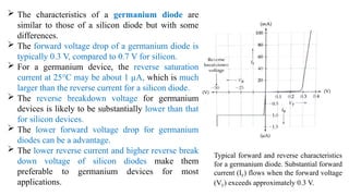
The characteristicsof a germanium diode are
similar to those of a silicon diode but with some
differences.
The forward voltage drop of a germanium diode is
typically 0.3 V, compared to 0.7 V for silicon.
For a germanium device, the reverse saturation
current at 25°C may be about 1 µA, which is much
larger than the reverse current for a silicon diode.
The reverse breakdown voltage for germanium
devices is likely to be substantially lower than that
for silicon devices.
The lower forward voltage drop for germanium
diodes can be a advantage.
The lower reverse current and higher reverse break
down voltage of silicon diodes make them
preferable to germanium devices for most
applications.
Typical forward and reverse characteristics
for a germanium diode. Substantial forward
current (IF) flows when the forward voltage
(VF) exceeds approximately 0.3 V.
15.
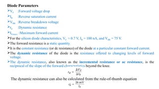
Diode Parameters
VF :Forwardvoltage drop
IR :Reverse saturation current
VBR :Reverse breakdown voltage
rd :Dynamic resistance
IF(max) :Maximum forward current
For the silicon diode characteristics, VF ≈ 0.7 V, IR = 100 nA, and VBR = 75 V.
The forward resistance is a static quantity.
It is the constant resistance (or dc resistance) of the diode at a particular constant forward current.
The dynamic resistance of the diode is the resistance offered to changing levels of forward
voltage.
The dynamic resistance, also known as the incremental resistance or ac resistance, is the
reciprocal of the slope of the forward characteristics beyond the knee.
The dynamic resistance can also be calculated from the rule-of-thumb equation
16.
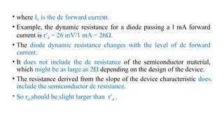
• where IFis the dc forward current.
• Example, the dynamic resistance for a diode passing a l mA forward
current is r′d = 26 mV/1 mA = 26Ω.
• The diode dynamic resistance changes with the level of dc forward
current.
• It does not include the dc resistance of the semiconductor material,
which might be as large as 2Ω depending on the design of the device.
• The resistance derived from the slope of the device characteristic does
include the semiconductor dc resistance.
• So rd should be slight larger than r′d .
17.
Problems
Calculate the forwardand reverse resistances offered by a silicon diode
with the characteristics, at IF = 100 mA and at VR = 50 V.
• Solution
18.
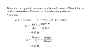
Determine the dynamicresistance at a forward current of 70 mA for the
diode characteristics. Estimate the diode dynamic resistance.
• Solution
19.
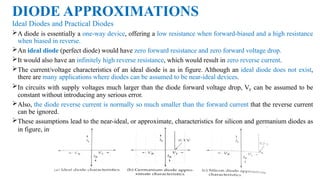
DIODE APPROXIMATIONS
Ideal Diodesand Practical Diodes
A diode is essentially a one-way device, offering a low resistance when forward-biased and a high resistance
when biased in reverse.
An ideal diode (perfect diode) would have zero forward resistance and zero forward voltage drop.
It would also have an infinitely high reverse resistance, which would result in zero reverse current.
The current/voltage characteristics of an ideal diode is as in figure. Although an ideal diode does not exist,
there are many applications where diodes can be assumed to be near-ideal devices.
In circuits with supply voltages much larger than the diode forward voltage drop, VF can be assumed to be
constant without introducing any serious error.
Also, the diode reverse current is normally so much smaller than the forward current that the reverse current
can be ignored.
These assumptions lead to the near-ideal, or approximate, characteristics for silicon and germanium diodes as
in figure, investigates a situation where the diode VF is assumed to be constant.
20.
Piecewise Linear Characteristic
Whenthe forward characteristic of a diode is not available, a straight-line
approximation called the piecewise linear characteristic may be employed.
To construct the piecewise linear characteristic, VF is first marked on the
horizontal axis, as shown in Figure.
Then, from VF, a straight line is drawn with a slope equal to the diode
dynamic resistance.
+
21.
DC Equivalent Circuits
An equivalent circuit for a device is a circuit that represents the device behavior.
The equivalent circuit is made up of a number of components, such as resistors and voltage cells.
A diode equivalent circuit may be substituted for the device when investigating a circuit containing
the diode. Equivalent circuits may also be used as device models for computer analysis.
A forward-biased diode is assumed to have a constant forward voltage drop (VF) and negligible
series resistance.
The diode equivalent circuit is assumed to be a voltage cell with a voltage VF.
A more accurate equivalent circuit includes the diode dynamic resistance (rd) in series with the
voltage cell. The small variations in VF that occur with change in forward current.
An ideal diode is also included to show that current flows only in one direction.
The equivalent circuit without rd assumes that the diode has the approximate characteristics.
23.
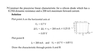
Construct the piecewiselinear characteristic for a silicon diode which has a
0.25Ω dynamic resistance and a 200 mA maximum forward current.
24.
Calculate IF forthe diode circuit in Fig.a assuming that the diode has VF= 0.7 V and rd =
0. Then recalculate the current taking rd = 0.25Ω.
25.
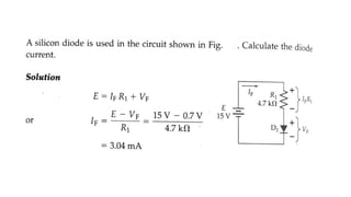
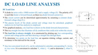
DC LOAD LINEANALYSIS
DC Load Line
A diode in series with a 100Ω resistor (R1) and a supply voltage (E). The polarity of E
is such that diode is forward-biased, so there is a diode forward current (IF).
The circuit current can be determined approximately by assuming a constant diode
forward voltage drop (VF).
The precise levels of the diode current and voltage must be calculated, graphical
analysis (or dc load line analysis) is employed.
For graphical analysis, a dc load line is drawn on the diode forward characteristics.
This is a straight line that illustrates all dc conditions that could exist within the circuit.
The load line is always straight, it is constructed by plotting any two corresponding
current and voltage points and then drawing a straight line through them.
To determine two points on the load line, an equation relating voltage, current, and
resistance is first derived for the circuit.
Any two convenient levels of IF can be substituted to calculate corresponding VF levels,
or vice versa. It is convenient to calculate VF when lF = 0, and to determine IF when VF
=0
E
26.
Draw the dcload line for the circuit in Fig. a on the diode forward
characteristic given in Fig. b
27.
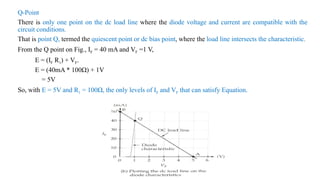
Q-Point
There is onlyone point on the dc load line where the diode voltage and current are compatible with the
circuit conditions.
That is point Q, termed the quiescent point or dc bias point, where the load line intersects the characteristic.
From the Q point on Fig., IF = 40 mA and VF =1 V,
E = (IF R1) + VF.
E = (40mA * 100Ω) + 1V
= 5V
So, with E = 5V and R1 = 100Ω, the only levels of IF and VF that can satisfy Equation.
28.
Calculating Load Resistanceand Supply Voltage
In a diode series circuit in Fig.a, resistor R1, dictates the slope of the dc load line, and supply voltage E
determines point A on the load line.
The circuit conditions can be altered by changing either R1 or E. Designing a diode circuit, it is
necessary to use a given supply voltage and set up a forward current.
In this case point A and Q are first plotted and the load line is drawn. Resistor R1 is then calculated from
the slope of the load line.
Example, R1 and the required IF are known, and the supply voltage is to be determined and is solved by
plotting point Q and drawing the load line with slope 1/R1. The supply voltage is then read at point A.
29.
Using the devicecharacteristics in Fig., determine the required load resistance for the circuit in
Fig.a to give IF = 30 mA.
30.
Determine a newsupply voltage for the circuit in Fig. to give a 50mA diode forward
current when R1 = 100Ω.
31.
Diode Applications
Most importantapplications of diodes is rectification. A rectifier is a
device that converts alternating current (ac) to direct current (dc).
RECTIFIERS
HALF WAVE RECTIFIERS FULL WAVE RECTIFIERS
BI-PHASE RECTIFIERS BRIDGE RECTIFIERS
32.
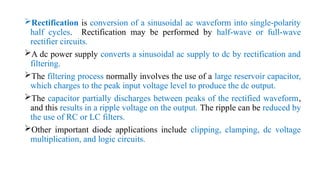
Rectification is conversionof a sinusoidal ac waveform into single-polarity
half cycles. Rectification may be performed by half-wave or full-wave
rectifier circuits.
A dc power supply converts a sinusoidal ac supply to dc by rectification and
filtering.
The filtering process normally involves the use of a large reservoir capacitor,
which charges to the peak input voltage level to produce the dc output.
The capacitor partially discharges between peaks of the rectified waveform,
and this results in a ripple voltage on the output. The ripple can be reduced by
the use of RC or LC filters.
Other important diode applications include clipping, clamping, dc voltage
multiplication, and logic circuits.
33.
HALF WAVE RECTIFICATION
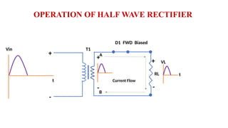
PositiveHalf-Wave Rectifier
An alternating input voltage is applied via a transformer (T1) to a single diode
connected in series with a load resistor RL.
The transformer is normally necessary to dc isolate the rectifier circuit from the ac
supply.
The diode is forward-biased during the positive half cycles of the input waveform,
and reverse-biased during the negative half cycles.
Substantial current flows through R only during the positive half cycles of the input.
For the duration of the negative half cycles, the diode behaves almost as an open
switch.
The output voltage waveform developed across RL is a series of positive half cycles of
alternating voltage with intervening very small negative voltage levels produced by the
diode reverse saturation current.
35.
OPERATION OF HALFWAVE RECTIFIER
T1
RL
D1
Vin
t
+
-
VL
t
FWD Biased
+
-
Current Flow
+
-
A
B
36.
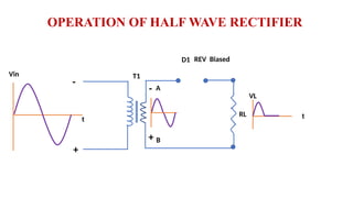
OPERATION OF HALFWAVE RECTIFIER
T1
RL
D1
Vin
t
+
-
VL
t
REV Biased
+
-
A
B
37.
WAVEFORMS OF HALFWAVE RECTIFIER
Vin
t
VL
t
D1 FWD
Biased
D1 REV
Biased
D1 FWD
Biased
D1 REV
Biased
Pulsating Output Voltage
38.
When the diodeis forward-biased, the voltage drop across it is VF, and the output voltage is (input voltage)
-VF. So, the peak output voltage(Vpo) is
Vpo = Vpi – VF
Note that Vpi = 1.414Vi, where Vi is the rms level of the sinusoidal input voltage to the rectifier circuit. The
diode peak forward current is
During the negative half-cycle of the input, the reverse-biased diode offers a very high resistance. So there
is only a very small reverse current (IR), giving an output voltage
-Vo=-IR RL
While the diode is reverse-biased, the peak voltage of the negative half-cycle of the input is applied to its
terminals. Thus the peak reverse voltage, or peak inverse voltage (PIV), applied to the diode is
VR= PIV= Vpi
The average and rms values of the half-wave rectified waveform can be determined as Vo(ave) = 0.318 Vpo
and Vo(rms) = 0.5 Vpo.
Rectifier circuits use a reservoir capacitor at the output terminals to smooth the rectified voltage wave into
direct voltage. It is very important to note that the presence of the capacitor changes the output waveform
and that it substantially affects the load current and voltage and the diode current and voltage.
39.
A diode withVF = 0.7 V is connected as a half-wave rectifier. The load
resistance is 500Ω, and the (rms) ac input is 22 V. Determine the peak output
voltage, the peak load current, and the diode peak reverse voltage.
40.
Negative Half-Wave Rectifier
Reversingthe diode polarity in the circuit the negative half-cycle of the ac input is passed to the
load resistor.
Consequently, the peak output voltage and current are negative quantities.
A positive half-wave rectifier circuit with the positive output terminal grounded. The ac input to
the rectifier circuit is normally derived from the secondary of a transformer. Either of the two
output terminals may be grounded so long as there is no other grounded point in the circuit.
When the transformer output waveform is at its peak positive level, the load waveform is actually a
peak negative quantity, because output terminal B is negative with respect to the grounded terminal
A.
Diode is reverse-biased during the negative half-cycle of the transformer output, so the load
voltage is zero.
A negative half-wave rectified waveform can be generated simply by grounding the positive output
terminal of a positive rectifier circuit.
One of the rectifier circuit output terminals may be grounded only when the transformer is present
to provide complete dc isolation from the ac supply.
If a variable transformer is used without a power supply transformer, a 1:1 isolation transformer
must be substituted for the power supply transformer to provide the required dc isolation
42.
FULL WAVE RECTIFICATION
Two-DiodeFull-Wave Rectifier
The full-wave rectifier circuit in Fig. uses two diodes, and its input voltage is supplied
from a transformer (T1) with a centre-tapped secondary winding. The circuit is
essentially a combination of two half-wave rectifier circuits, each supplied from one
half of the transformer secondary.
43.
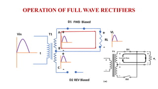
OPERATION OF FULLWAVE RECTIFIERS
T1
A
D1
+
-
VL
FWD Biased
+
-
B
C
D2
RL
Vin
t
REV Biased
+
-
44.
OPERATION OF FULLWAVE RECTIFIERS
T1
A
D1
+
-
vout
REV Biased
+
-
B
C
D2
RL
vin
t
FWD Biased
+
-
45.
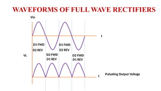
WAVEFORMS OF FULLWAVE RECTIFIERS
Vin
t
VL
t
D1 FWD
D2 FWD
Pulsating Output Voltage
D2 REV
D1 REV
D1 FWD
D2 REV
D2 FWD
D1 REV
46.
When the transformeroutput voltage is positive at the top, the anode of D1, is positive, and the centre
tap of the transformer is connected to the cathode of D1 by RL.
Consequently, D1 is forward-biased, and load current (IL) flows from the top of the transformer
secondary through D1, through RL from top to bottom, and back to the transformer centre tap. During
this time, the polarity of the voltage from the bottom half of the transformer secondary causes diode
D2, to be reverse-biased.
Duration of the negative half-cycle of the transformer output, the polarity of the transformer secondary
voltage causes D1, to be reverse-biased and D2, to be forward-biased.
IL flows from the bottom terminal of the transformer secondary through diode D2 through RL from top
to bottom, and back to the transformer centre tap.
The output waveform is the combination of the two half-cycles, that is, a continuous series of positive
half cycles of sinusoidal waveform. This is positive full-wave rectification.
47.
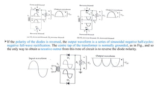
If the polarityof the diodes is reversed, the output waveform is a series of sinusoidal negative half-cycles:
negative full-wave rectification. The centre tap of the transformer is normally grounded, as in Fig., and so
the only way to obtain a negative output from this type of circuit is to reverse the diode polarity.
48.
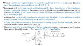
Bridge Rectifier
The centre-tappedtransformer used in the circuit of Fig. is usually more expensive and requires
more space than additional diodes.
So a bridge rectifier is the circuit most frequently used for full-wave rectification.
The bridge rectifier circuit in Fig. is seen to consist of four diodes connected with their
arrowhead symbols all pointing toward the positive output terminal of the circuit.
Diodes D1 and D2 are series-connected, as are D3 and D4. The ac input terminals are the junction
of D1 and D2 and the junction of D3 and D4.
The positive output terminal is at the cathodes of D1, and D3, and the negative output is at the
anodes of D2, and D4.
50.
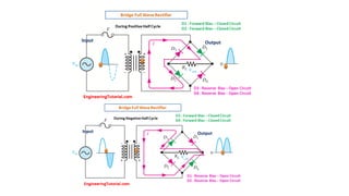
During the positivehalf-cycle of input voltage, diodes D1 and D4 are in series with RL
Load current (IL) flows from the positive input terminal through D1 to RL, and then
through RL and D4, back to the negative input terminal. The direction of the load Current
through RL is from top to bottom.
The positive input terminal is applied to the cathode of D2, and the negative output is at
the D2 anode. So D2 is reverse-biased during the positive half-cycle of the input.
Similarly, D3 has the negative input at its anode and the positive output at its cathode
during the positive input half-cycle, causing D3, to be reverse-biased.
Diodes D2 and D3 are forward-biased during the negative half-cycle of the input
waveform, while D1 and D4 are reverse biased. Although the input terminal polarity is
reversed, IL again lows through RL, from top to bottom, via D3 and D2.
During both half-cycles of the input, the output terminal polarity is always positive at the
top of RL, and negative at the bottom. Both positive and negative half-cycles of the input
are passed to the output.
The negative half-cycles are inverted, so that the output is a continuous series of positive
half-cycles of sinusoidal voltage.
52.
Operation of BridgeRectifier
T1
RL
vin
t
vout
D1
D2
D3
D4
A
B
+
-
-
+
FWD
FWD
REV
REV
t
-
+
53.
Operation of BridgeRectifier
T1
RL
vin
t vout
D1
D2
D3
D4
-
A
B +
FWD
FWD
REV
REV
+
- t
54.
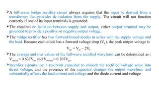
A full-wave bridgerectifier circuit always requires that the input be derived from a
transformer that provides dc isolation from the supply. The circuit will not function
correctly if one of its input terminals is grounded.
The required dc isolation between supply and output, either output terminal may be
grounded to provide a positive or negative output voltage.
The bridge rectifier has two forward-biased diodes in series with the supply voltage and
the load. Because each diode has a forward voltage drop (VF), the peak output voltage is
Vpo = Vpi – 2VF
The average and rms values of the full-wave rectified waveform can be determined as :
Vo(ave) = 0.637Vpo and Vo(rms) = 0.707Vpo.
Rectifier circuits use a reservoir capacitor to smooth the rectified voltage wave into
direct voltage, and the presence of the capacitor changes the output waveform and
substantially affects the load current and voltage and the diode current and voltage.
55.
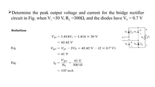
Determine the peakoutput voltage and current for the bridge rectifier
circuit in Fig. when Vi =30 V, RL =300Ω, and the diodes have VF = 0.7 V
56.
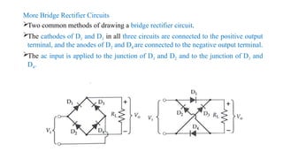
More Bridge RectifierCircuits
Two common methods of drawing a bridge rectifier circuit.
The cathodes of D1 and D3 in all three circuits are connected to the positive output
terminal, and the anodes of D2 and D4 are connected to the negative output terminal.
The ac input is applied to the junction of D1 and D2 and to the junction of D3 and
D4.
57.
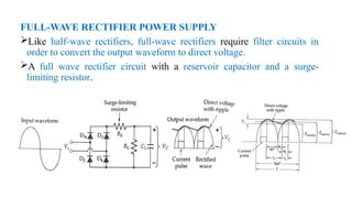
FULL-WAVE RECTIFIER POWERSUPPLY
Like half-wave rectifiers, full-wave rectifiers require filter circuits in
order to convert the output waveform to direct voltage.
A full wave rectifier circuit with a reservoir capacitor and a surge-
limiting resistor.
58.
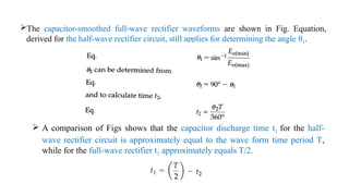
The capacitor-smoothed full-waverectifier waveforms are shown in Fig. Equation,
derived for the half-wave rectifier circuit, still applies for determining the angle θ1.
A comparison of Figs shows that the capacitor discharge time t1 for the half-
wave rectifier circuit is approximately equal to the wave form time period T,
while for the full-wave rectifier t1 approximately equals T/2.
59.
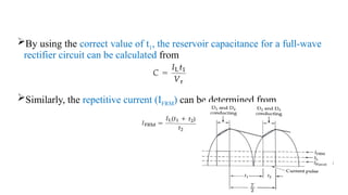
By using thecorrect value of t1, the reservoir capacitance for a full-wave
rectifier circuit can be calculated from
Similarly, the repetitive current (IFRM) can be determined from
60.
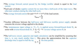
The average forwardcurrent passed by the bridge rectifier circuit is equal to the load
current.
Each pair of diodes supplies current for no more than a half-cycle of the input wave. The
other pair conducts during the other half cycle.
The average forward current for each diode is half of the load current.
Another difference between the half-wave and full-wave rectifier power supply circuits
concerns the reverse voltage applied to the diodes.
The instantaneous input voltage is +Vp, Vp, is applied across forward-biased diode D1, in
series with reverse-biased diode D3. Therefore, the reverse voltage across D3 is
The half-wave circuit, capacitor and ripple calculations can be simplified by assuming that
time t2, is very much smaller than t1. This gives the approximation that the capacitor
discharge time is equal to half the input waveform time period.
61.
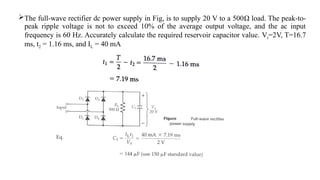
The full-wave rectifierdc power supply in Fig, is to supply 20 V to a 500Ω load. The peak-to-
peak ripple voltage is not to exceed 10% of the average output voltage, and the ac input
frequency is 60 Hz. Accurately calculate the required reservoir capacitor value. Vr=2V, T=16.7
ms, t2 = 1.16 ms, and IL = 40 mA
62.
Assuming that t2is very much smaller than t1, for the full-wave rectifier circuit , recalculate
the required reservoir capacitor value. Vr=2V, T=16.7 ms and IL = 40 mA
63.
Specify the diodesfor the bridge rectifier circuit in Ex. Select a suitable
device and calculate the surge-limiting resistance.
From Datasheet of diode
IFSM = 30A
64.
Transformer Selection
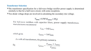
The transformerspecification for a full-wave bridge rectifier power supply is determined
similarly to that for a half-wave circuit, with some exceptions.
Two diode voltage drops are involved in calculating the secondary rms voltage.
65.
Specify the transformerfor the full-wave rectifier power supply circuit in Example. IL =
40 mA, VP(rms) = 115V, 60 Hz
66.
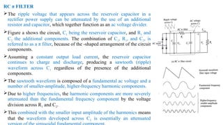
RC π FILTER
Theripple voltage that appears across the reservoir capacitor in a
rectifier power supply can be attenuated by the use of an additional
resistor and capacitor, which together function as an ac voltage divider.
Figure a shows the circuit, C1 being the reservoir capacitor, and R1 and
C2 the additional components. The combination of C1, R1, and C2, is
referred to as a π filter, because of the -shaped arrangement of the circuit
components.
Assuming a constant output load current, the reservoir capacitor
continues to charge and discharge, producing a sawtooth (ripple)
waveform across C1 regardless of the presence of the additional
components.
The sawtooth waveform is composed of a fundamental ac voltage and a
number of smaller-amplitude, higher-frequency harmonic components.
Due to higher frequencies, the harmonic components are more severely
attenuated than the fundamental frequency component by the voltage
division across R1 and C2.
This combined with the smaller input amplitude of the harmonics means
that the waveform developed across C2 is essentially an attenuated
67.
By Fourier analysis,peak value of fundamental component of the sawtooth waveform is
where Vr, is the ripple voltage peak-to-peak amplitude
The ac voltage developed across C2 is the filter ac output and is given by
The additional attenuation of the ripple voltage depends upon the selection of R1 and C2 values.
There is a dc voltage drop across R1 produced by the output current (VR1), and this must be
considered when determining a suitable resistance for R1.
68.
The 2 Vripple waveform across capacitor C1 in Ex. is to be further attenuated by the use of an
additional resistor and capacitor, as in Fig. If R1 = 22Ω and C1 = C2= 150 µF, calculate the dc output
voltage and the output ripple amplitude. IL = 40 mA, fr = 120Hz.
69.
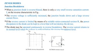
ZENER DIODES
Junction Breakdown
Whena junction diode is reverse-biased, there is only a very small reverse saturation current:
Is on the reverse characteristic in Fig..
The reverse voltage is sufficiently increased, the junction breaks down and a large reverse
current flows.
If the reverse current is limited by means of a suitable series-connected resistor R1 the power
dissipation in the diode can be kept to a level that will not destroy the device.
The diode may be operated continuously in reverse breakdown. The reverse current returns to
its normal level when the voltage is reduced below the reverse breakdown level.
70.
Diodes designed foroperation in reverse breakdown are found to have breakdown voltage
that remains extremely stable over a wide range of current levels.
With a very narrow depletion region, the electric field strength produced by a reverse bias
voltage can be very high.
The high-intensity electric field causes electrons to break away from their atoms, thus
converting the depletion region from an insulating material into a conductor.
This is ionization by electric field, also called Zener breakdown, and it usually occurs
with reverse bias voltages less than 5 V.
Where the depletion region is too wide for Zener breakdown, the electrons in the reverse
saturation current can be given sufficient energy to cause other electrons to break free
when they strike atoms within the depletion region. This is termed ionization by collision.
The electrons released in this way collide with other atoms to produce more free electrons
in an avalanche effect. Avalanche breakdown is normally produced by reverse voltage
levels above 5 V.
Zener and avalanche are two different types of break down.
71.
Circuit Symbol andPackage
The circuit symbol for a Zener diode in Fig. (a) is with the cathode bar approximately in the shape
of a letter Z.
Arrowhead on the symbol points the direction of forward current when the device is forward-
biased.
In reverse bias, the voltage drop (Vz) is positive (+) on the cathode and negative (-) on the anode.
Low-power Zener diodes the coloured band identifies the cathode terminal, as in the case of an
ordinary low-current diode. High-current Zener diodes are also available.
72.
Characteristics and Parameters
Typicalcharacteristics of a Zener diode are shown in detail in Fig.. The forward characteristic is simply that
of an ordinary forward-biased diode.
Some important points on the reverse characteristic are
Vz : Zener breakdown voltage
IZT :Test current for measuring
VZK :Reverse current near the knee of the characteristic, the minimum reverse current to sustain breakdown
IZM : Maximum Zener current, limited by the maximum power dissipation
73.
The dynamic impedance(Zz) is:
As in Fig., Zz defines how Vz changes with variations in diode reverse
current.
When measured at IZT, the dynamic impedance is designated (ZZT). The
dynamic impedance measured at the knee of the characteristic (ZZK) is
substantially larger than ZZT.
The Zener diode may be operated at any (reverse) current level between IZK
and lZM.
For greatest voltage stability, the diode is normally operated at the test
current (lZT). Many low-power Zener diodes have a test current specified as
20 mA; however, some devices have lower test currents.
74.
Equivalent Circuit
The dcequivalent circuit for a Zener diode is simply a voltage cell with a
voltage Vz, as in Fig..
The equivalent circuit for the device for all dc calculations.
For the ac equivalent circuit (Fig.), the dynamic impedance is included in series
with the voltages cell.
The ac equivalent circuit is used in situations where the Zener current is varied
by small amounts. The Zener diode is maintained in reverse breakdown.
75.
A Zener diodewith Vz=4.3 V has Zz equal to 22Ω when lz = 20 mA. Calculate the
upper and lower limits of Vz when Iz changes by ±5mA.
76.
ZENER DIODE VOLTAGEREGULATORS
Regulator Circuit with No Load
The most important application of Zener diodes is in dc voltage
regulator circuits.
The circuit is usually employed as a voltage reference source
that supplies only a very low current (much lower than Iz) to the
output.
Resistor R1 limits the Zener diode current to the desired level. Iz
is calculated as follows:
The Zener current may be just greater than the diode knee
current (lZK).
For the most stable reference voltage, IZ should be selected as IZT
77.
A 9 Vreference source is to use a series-connected Zener diode and resistor connected to a 30 V supply.
Select suitable components, and calculate the circuit current when the supply voltage drops to 27 V.
Solution:
Data sheet for Zener diodes, shows that the most suitable device is a 1N757, which has Vz =9.1 V and Izr = 20
mA.
78.
Loaded Regulator
Zener dioderegulator has to supply a load current (IL), as the total supply
current is the sum of IL and lZ.
Care must be taken to ensure that the minimum Zener diode current is large
enough to keep the diode in reverse break down. Typically, Iz(min) = 5 mA
for a Zener diode with an IZT of 20 mA. The circuit current equation is
The load current in the circuit may be reduced to zero.
The voltage drop aross R remains constant, the supply current remains
constant.
This current flows through the Zener diode when RL is disconnected. The
circuit design must ensure that the total current does not exceed the
maximum Zener diode current.
79.
Design a 6V dc reference source to operate from a 16 V supply. The circuit is to use a low-
power Zener diode and is to produce the maximum possible load current. Calculate the
maximum load current that can be taken from the circuit. Vz= 6.2 V and PD = 400 mW.
80.
Regulator Performance
The performanceof a Zener diode voltage regulator may be expressed in
terms of the source and load effects and the line and load regulations.
If there is an input ripple voltage, it will be severely attenuated. The ripple
rejection ratio is the ratio of the output to input ripple amplitudes.
To assess the performance of a Zener diode voltage regulator, the ac
equivalent circuit is first drawn by replacing the diode with its dynamic
impedance (Zz).
The complete ac equivalent circuit seen to be a simple voltage divider. When
the input voltage changes by ΔEs, the output voltage change is
When there is a load, RL appears in parallel with Zz in the ac equivalent
circuit (Fig.). The equation for the output voltage change now becomes
81.
The input rippleamplitude (Vri) and the output ripple (Vro) are substituted for the input and
output voltages thus, Eq. can be modified to give a ripple rejection ratio equation,
To determine the load effect of the Zener diode voltage regulator, the circuit output
resistance has to be calculated.
The regulator Thevenin equivalent circuit in Fig. shows that, assuming a zero source
resistance, the Circuit output resistance is
The load current changes by ΔIL, the output voltage change is
82.
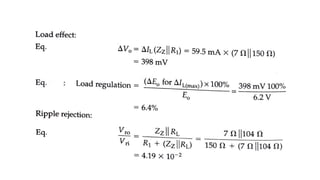
Example 3-18 Calculatethe line regulation, load regulation, and ripple rejection ratio for the voltage
regulator. ZZ =7Ω.
Source effect:


![Course outcome
(Course Skill
Set)
At the end of the course the student will be able to:
CO1: Develop the basic knowledge on construction,
operation and characteristics of semiconductor devices.
[K3]
CO2: Apply the acquired knowledge to construct small
scale circuits consisting of semiconductor devices. [K3]
CO3: Develop competence knowledge to construct basic
digital circuit by make use of basic gate and its function.
[K3]
CO4: Construct the conceptual blocks for basic
communication system. [K3]
CO5: Apply the knowledge of various transducers principle
in sensor system.[K3]](https://image.slidesharecdn.com/module1basicelectronicsbbee203lmb1-250504123219-e35da6b6/85/Module-1_Basic-Electronics_BBEE203_LMB-1-pptx-6-320.jpg)