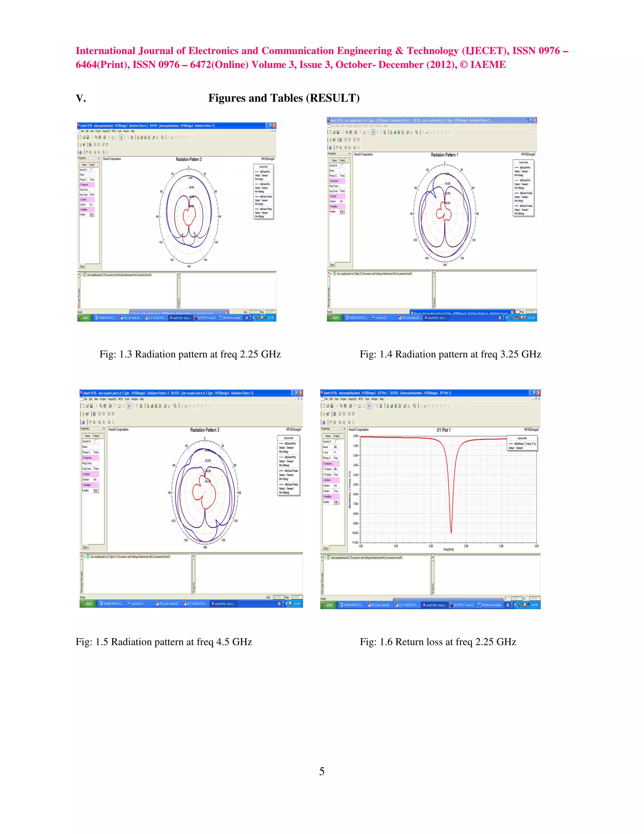
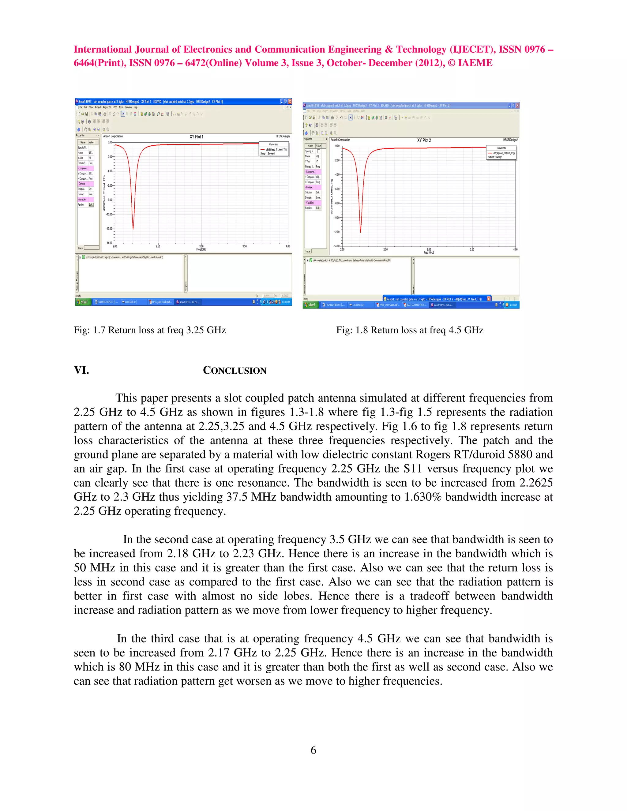
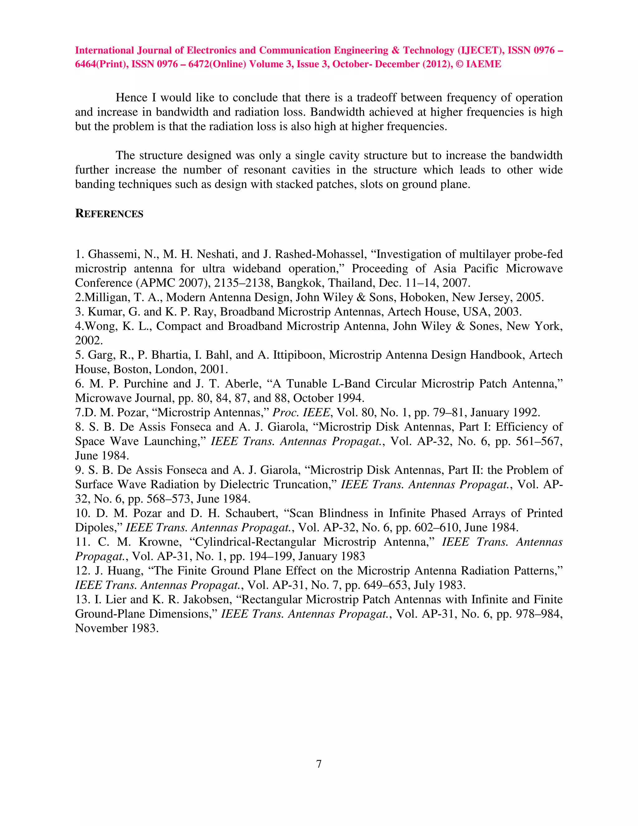
The document summarizes research on simulating and analyzing a slot-coupled patch antenna at different frequencies using HFSS software. It describes the structure of the antenna, which consists of a rectangular patch separated from the ground plane by an air gap and dielectric material. The antenna is fed by two slots on the ground plane. Simulation results showed that bandwidth increases at higher frequencies but radiation patterns deteriorate. There is thus a tradeoff between operating frequency, bandwidth, and radiation efficiency. The design was able to achieve bandwidth increases up to 80 MHz at 4.5 GHz but radiation patterns worsened compared to lower frequencies.
![International Journal of Electronics and Communication Engineering AND COMMUNICATION0976 –
INTERNATIONAL JOURNAL OF ELECTRONICS & Technology (IJECET), ISSN
6464(Print), ISSN 0976 – 6472(Online) Volume& Issue 3, October- December (2012), © IAEME
ENGINEERING 3, TECHNOLOGY (IJECET)
ISSN 0976 – 6464(Print)
ISSN 0976 – 6472(Online)
Volume 3, Issue 3, October- December (2012), pp. 01-07 IJECET
© IAEME: www.iaeme.com/ijecet.html
Journal Impact Factor (2012): 3.5930 (Calculated by GISI) ©IAEME
www.jifactor.com
SIMULATION AND ANALYSIS OF SLOT-COUPLED PATCH ANTENNA
AT DIFFERENT FREQUENCIES USING HFSS
Tauheed Qamar1, Naseem Halder2, Mohd. Gulman Siddiqui3, Vishal Varshney4
1,2,,3,4
(Department of Electronics and Communication Engineering
Amity School of Engineering And Technology, Amity University, Noida, U.p, India
1
(muhammadtauheed20@gmail.com), 2(naseem.halder@yahoo.in),
3
(mohdgulman@gmail.com ) ,4(vishal.amity08@yahoo.co.in )
ABSTRACT
Microstrip patch antennas are well suited for integration in too many applications owing to their
conformal nature. There are many wide banding techniques used for the MSAs. But many wide
banding techniques such as using slots in the patch require an inductive coupled feed. Aperture
coupled feed which makes use of thick antenna substrates is the most convenient as it has only
single ground plane. Apart from this aperture coupling provides a greater radiation pattern
symmetry and greater ease of design for higher impedance band width owing to a large number
of design parameters. In this type of feed by using multiple patches bandwidths up to 70% are
reported. This paper presents a slot coupled microstrip antenna with a rectangular patch which is
located on top of two slots on the ground plane. The patch and slots are separated by an air gap
and a material with low dielectric constant. The reduction in return loss is achieved as we moved
to the higher frequencies. The operational frequencies are taken as from 3 GHz to 5 GHz. The
comparison of s parameter plot and radiation pattern plot is done in order to achieve a better
design in terms of low return loss, improved radiation pattern etc.
Keywords – Air gap, Aperture coupled, High bandwidth, MSA, Radiation pattern, Return loss &
S-parameter.
I. INTRODUCTION
Microstrip antennas have several advantages like: low cost, easy fabrication and light weight.
But they suffer from disadvantages like low gain and narrow impedance bandwidth [1-5]. In
high-performance aircraft, spacecraft, satellite, and missile applications, where size, weight, cost,
1](https://image.slidesharecdn.com/simulationandanalysisofslotcoupledpatchantenna-121220235751-phpapp01/75/Simulation-and-analysis-of-slot-coupled-patch-antenna-1-2048.jpg)
![International Journal of Electronics and Communication Engineering & Technology (IJECET), ISSN 0976 –
6464(Print), ISSN 0976 – 6472(Online) Volume 3, Issue 3, October- December (2012), © IAEME
performance, ease of installation, and aerodynamic profile are constraints, and low-profile
antennas may be required. Presently there are many other government and commercial
applications, such as mobile radio and wireless communications that have similar specifications.
To meet these requirements, microstrip antennas can be used [7]. These antennas are low profile,
conformable to planar and non planar surfaces, simple and inexpensive to manufacture using
modern printed-circuit technology, mechanically robust when mounted on rigid surfaces,
compatible with MMIC designs, and when the particular patch shape and mode are selected, they
are very versatile in terms of resonant frequency, polarization, pattern, and impedance [6]. In
addition, by adding loads between the patch and the ground plane, such as pins and varactor
diodes, adaptive elements with variable resonant frequency, impedance, polarization, and pattern
can be designed.
Major operational disadvantages of microstrip antennas are their low efficiency, low
power, high Q (sometimes in excess of 100), poor polarization purity, poor scan performance,
spurious feed radiation and very narrow frequency bandwidth, which is typically only a fraction
of a percent or at most a few percent. In some applications, such as in government security
systems, narrow bandwidths are desirable [7]. However, there are methods, such as increasing
the height of the substrate that can be used to extend the efficiency (to as large as 90 percent if
surface waves are not included) and bandwidth (up to about 35 percent). However, as the height
increases, surface waves are introduced which usually are not desirable because they extract
power from the total available for direct radiation (space waves). The surface waves travel within
the substrate and they are scattered at bends and surface discontinuities, such as the truncation of
the dielectric and ground plane [8 & 13], and degrade the antenna pattern and polarization
characteristics. Surface waves can be eliminated, while maintaining large bandwidths, by using
cavities. Stacking, as well as other methods, of microstrip elements can also be used to increase
the bandwidth.
In addition, microstrip antennas also exhibit large electromagnetic signatures at certain
frequencies outside the operating band, are rather large physically at VHF and possibly UHF
frequencies, and in large arrays there is a trade-off between bandwidth and scan volume. In order
to achieve the higher bandwidth with improved radiation efficiency and reduced return loss, slot
couple patch antenna is design in such a manner that it can easily overcome these problems [10].
II. RESEARCH METHODOLOGY
The research methodology inculcates the designing of the slot couple patch antenna. This
designed antenna structure is fed by using single coaxial probe feed. After feeding the antenna
structure these designed antennas are further simulated over HFSS simulation software, a FET
based simulation software. These simulations are continued till an optimum result is obtained.
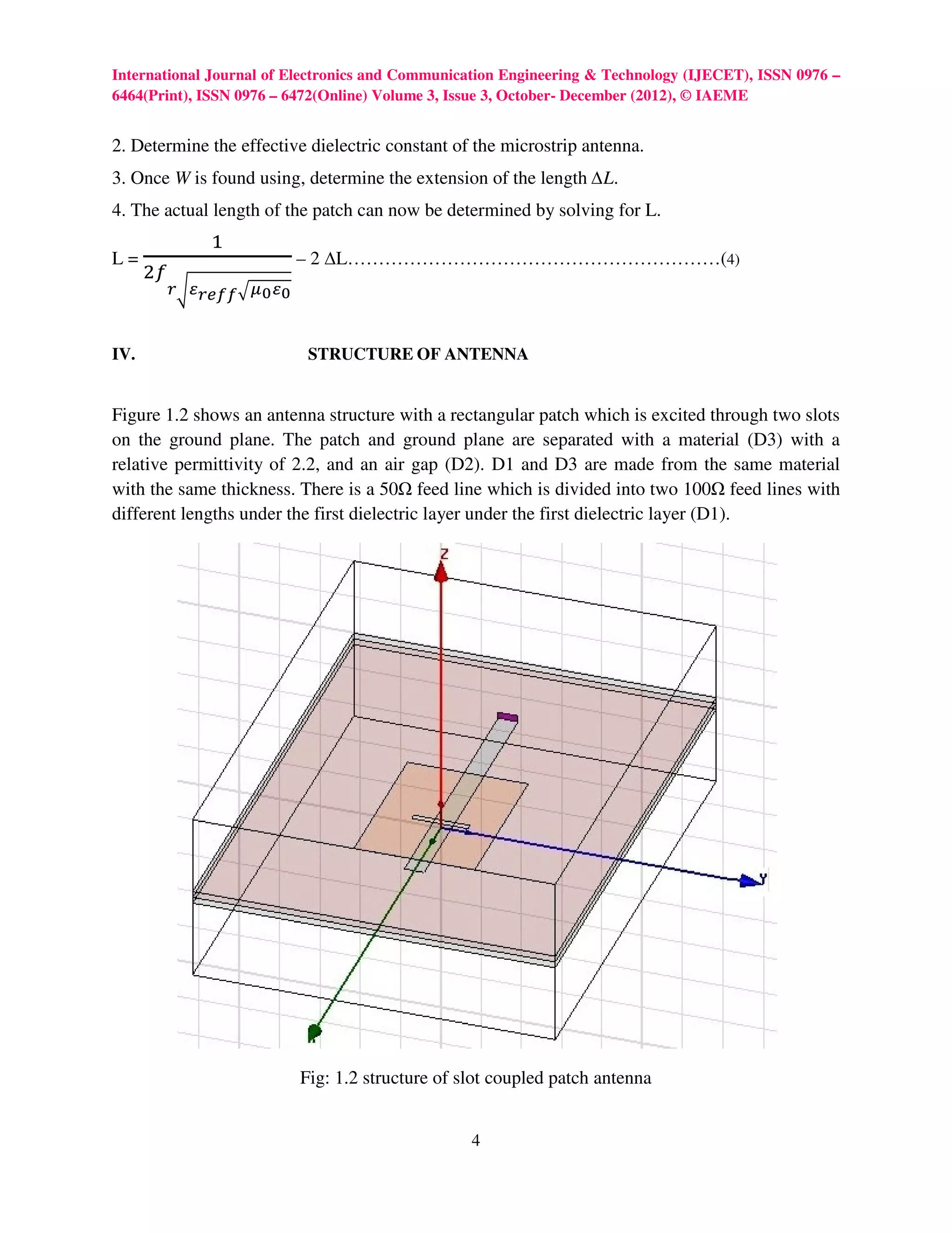
III. INDENTATIONS AND EQUATIONS (ANTENNA DESIGN):
Because of the fringing effects, electrically the patch of the microstrip antenna looks
greater than its physical dimensions. For the principal E-plane (xy-plane), this is demonstrated in
Figure 1.1 where the dimensions of the patch along its length have been extended on each end by
2](https://image.slidesharecdn.com/simulationandanalysisofslotcoupledpatchantenna-121220235751-phpapp01/75/Simulation-and-analysis-of-slot-coupled-patch-antenna-2-2048.jpg)
![International Journal of Electronics and Communication Engineering & Technology (IJECET), ISSN 0976 –
6464(Print), ISSN 0976 – 6472(Online) Volume 3, Issue 3, October- December (2012), © IAEME
a distance ∆L, which is a function of the effective dielectric constant εreff and the width-to-height
ratio (W/h).
∆L ∆L
L
W
Figure: 1.1 Physical and effective lengths of rectangular microstrip patch.
A very popular and practical approximate relation for the normalized extension of the length is
given by the following expression:
∆L/h = 0.412 {(εreff+0.3)[(W/h)+0.264]/ (εreff+0.3)[(W/h)+0.264]}…….(1)
Since the length of the patch has been extended by ∆L on each side, the effective length of
the patch is now (L = λ/2 for dominant TM010 mode with no fringing)
Leffe = L+2∆L……………………………………………..(2)
Based on the simplified formulation that has been described, a design procedure is outlined
which leads to practical designs of rectangular microstrip antennas. The procedure assumes that
the specified information includes the dielectric constant of the substrate (εr), the resonant
frequency (fr), and the height of the substrate h. The procedure is as follows: Specify: εr, fr (in
Hz), and h. Determine: W, L
Design Equations:
1. For an efficient radiator, a practical width that leads to good radiation efficiencies is
W = ( 1/(2frඥߤ ߝ )ඥ2/(ߝ + 1) = (ݒ /2݂ ) ඥ2/(ߝ + 1) ............................(3)
Where vo is the free-space velocity of light.
3](https://image.slidesharecdn.com/simulationandanalysisofslotcoupledpatchantenna-121220235751-phpapp01/75/Simulation-and-analysis-of-slot-coupled-patch-antenna-3-2048.jpg)