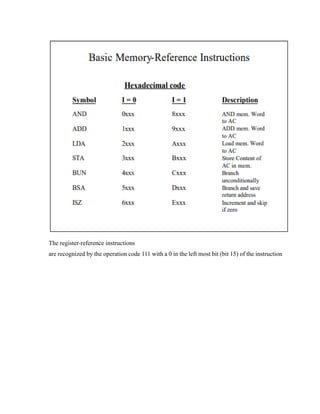
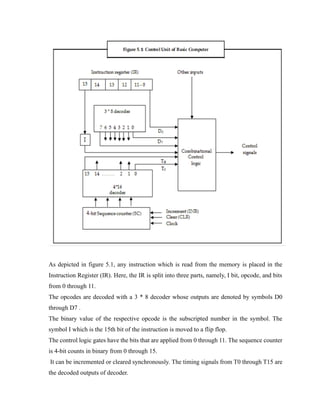
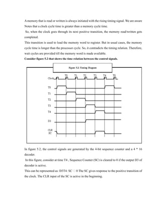
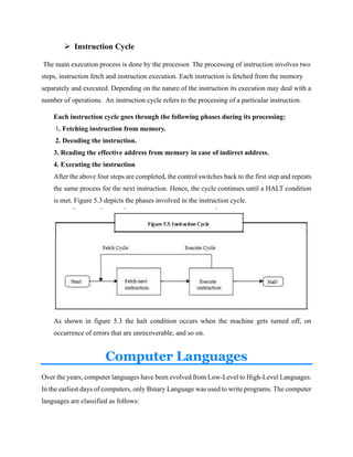
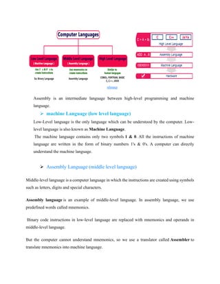
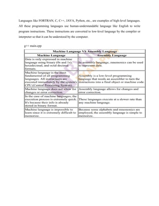
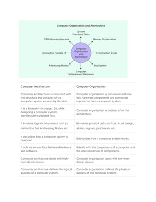
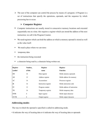
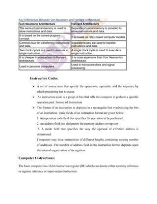
This document provides information on computer organization and design. It discusses the basic components of a computer system including the CPU, memory, I/O devices, and how they interconnect. It also describes different types of computer architecture like Von Neumann and Harvard architectures. Additionally, it covers topics like instruction codes, addressing modes, instruction cycles, and levels of programming languages from low-level machine code to high-level languages.

![I. Memory Reference – These instructions refer to memory address as an operand. The other
operand is always accumulator.
Specifies 12-bit address, 3-bit opcode (other than 111) and 1 bit addressing mode for direct
and indirect addressing.
Example – IR register contains = 0001XXXXXXXXXXXX, i.e., ADD after fetching and
decoding of instruction we find out that it is a memory reference instruction for ADD
operation.
Hence, DR <- M[AR] AC <- AC+ DR, SC <- 0
II. Register Reference – These instructions perform operations on registers rather than
memory addresses.
The IR (14-12) is 111 (differentiates it from memory reference) and IR (15) is 0 (differentiates
it from input/output instructions).
The rest 12 bits specify register operation. Example – IR register contains =
0111001000000000, i.e., CMA after fetch and decode cycle we find out that it is a register
reference instruction for complement accumulator. Hence, AC <- ~AC
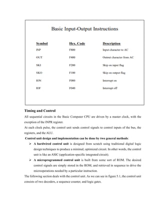
III. Input/Output – These instructions are for communication between computer and outside
environment.
The IR (14-12) is 111 (differentiates it from memory reference) and IR (15) is 1 (differentiates
it from register reference instructions). The rest 12 bits specify I/O operation. Example – IR
register contains = 1111100000000000, i.e., INP after fetch and decode cycle we find out that
it is an input/output instruction for inputting character. Hence, INPUT character from
peripheral device
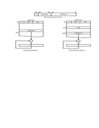
Direct and Indirect Addressing Modes
➢ When the second part specifies the address of an operand, the instruction is said to have
direct address.
➢ This is in contrast to a third possibility called indirect address, where the bits in the
second part of the instruction designate an address of memory word in which the address
of the operand is found.](https://image.slidesharecdn.com/chapter3ce-240107054709-23e44a69/85/Chapter-3-computer-organization-and-artpdf-8-320.jpg)