COMPUTER ORGANIZATION &
ARCHITECTURE
(BCS-DS-402)
1.2Instruction execution cycle
Ms. Swati Hans,
Assistant Professor
Department of Computer Science &
Engineering- SPL
School of Engineering & Technology
Manav Rachna International Institute of
Research and Studies (Deemed to be
University), Faridabad
2.
Instruction Codes
A processis controlled by a program
A program is a set of instructions that
specify the operations, data, and the
control sequence
An instruction is stored in binary code that
specifies a sequence of microoperations
Instruction codes together with data are
stored in memory (Stored Program
Concept)
3.
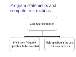
Program statements and
computerinstructions
Computer instruction
Field specifying the
operation to be executed
Field specifying the data
To be operated on
4.
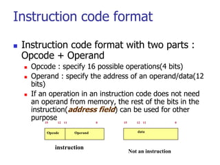
Instruction code format
Instruction code format with two parts :
Opcode + Operand
Opcode : specify 16 possible operations(4 bits)
Operand : specify the address of an operand/data(12
bits)
If an operation in an instruction code does not need
an operand from memory, the rest of the bits in the
instruction(address field) can be used for other
purpose
Opcode Operand
15 12 11 0
instruction
data
15 12 11 0
Not an instruction
5.
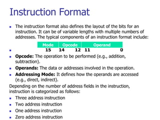
Instruction Format
Theinstruction format also defines the layout of the bits for an
instruction. It can be of variable lengths with multiple numbers of
addresses. The typical components of an instruction format include:
15 14 12 11 0
Opcode: The operation to be performed (e.g., addition,
subtraction).
Operands: The data or addresses involved in the operation.
Addressing Mode: It defines how the operands are accessed
(e.g., direct, indirect).
Depending on the number of address fields in the instruction,
instruction is categorized as follows:
Three address instruction
Two address instruction
One address instruction
Zero address instruction
Mode Opcode Operand
6.
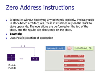
Zero Address instructions
It operates without specifying any operands explicitly. Typically used
in stack-based architectures, these instructions rely on the stack to
store operands. The operations are performed on the top of the
stack, and the results are also stored on the stack.
Example
Uses Postfix Notation of expression
Push A
Push B
7.
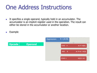
One Address Instructions
It specifies a single operand, typically held in an accumulator. The
accumulator is an implicit register used in the operation. The result can
either be stored in the accumulator or another location.
Example
Opcode Operand
8.
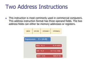
Two Address Instructions
This instruction is most commonly used in commercial computers.
This address instruction format has three operand fields. The two
address fields can either be memory addresses or registers.
9.
Three Address Instructions
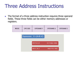
The format of a three address instruction requires three operand
fields. These three fields can be either memory addresses or
registers.
10.
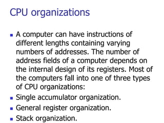
CPU organizations
Acomputer can have instructions of
different lengths containing varying
numbers of addresses. The number of
address fields of a computer depends on
the internal design of its registers. Most of
the computers fall into one of three types
of CPU organizations:
Single accumulator organization.
General register organization.
Stack organization.
11.
Single Accumulator Organization
All the operations on a system are performed with an
implied accumulator register. The instruction format in
this type of computer uses one address field.
For example, the instruction for arithmetic addition is
defined by an assembly language instruction ‘ADD.’
Where X is the operand’s address, the ADD instruction
results in the operation.
AC ← AC + M[X].
AC is the accumulator register, M[X] symbolizes the
memory word located at address X.
12.
General Register Organization
The general register type computers employ two or
three address fields in their instruction format. Each
address field specifies a processor register or a memory.
An instruction symbolized by ADD R1, X specifies the
operation R1 ← R + M [X].
This instruction has two address fields: register R1 and
memory address X.
13.
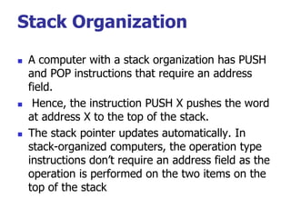
Stack Organization
Acomputer with a stack organization has PUSH
and POP instructions that require an address
field.
Hence, the instruction PUSH X pushes the word
at address X to the top of the stack.
The stack pointer updates automatically. In
stack-organized computers, the operation type
instructions don’t require an address field as the
operation is performed on the two items on the
top of the stack
14.
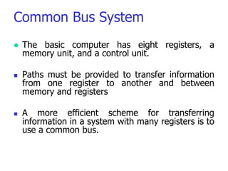
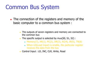
Common Bus System
The basic computer has eight registers, a
memory unit, and a control unit.
Paths must be provided to transfer information
from one register to another and between
memory and registers
A more efficient scheme for transferring
information in a system with many registers is to
use a common bus.
Common Bus System
The connection of the registers and memory of the
basic computer to a common bus system :
The outputs of seven registers and memory are connected to
the common bus
The specific output is selected by mux(S0, S1, S2) :
Memory(7), AR(1), PC(2), DR(3), AC(4), IR(5), TR(6)
When LD(Load Input) is enable, the particular register
receives the data from the bus
Control Input : LD, INC, CLR, Write, Read
17.
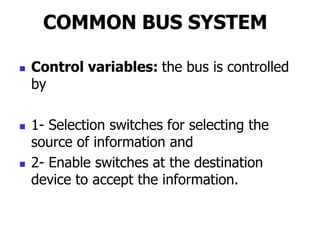
COMMON BUS SYSTEM
Control variables: the bus is controlled
by
1- Selection switches for selecting the
source of information and
2- Enable switches at the destination
device to accept the information.
18.
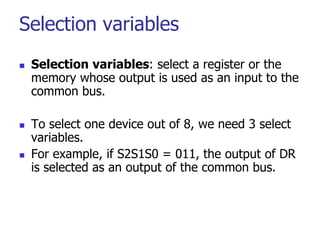
Selection variables
Selectionvariables: select a register or the
memory whose output is used as an input to the
common bus.
To select one device out of 8, we need 3 select
variables.
For example, if S2S1S0 = 011, the output of DR
is selected as an output of the common bus.
19.
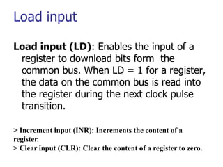
Load input
Load input(LD): Enables the input of a
register to download bits form the
common bus. When LD = 1 for a register,
the data on the common bus is read into
the register during the next clock pulse
transition.
> Increment input (INR): Increments the content of a
register.
> Clear input (CLR): Clear the content of a register to zero.
20.
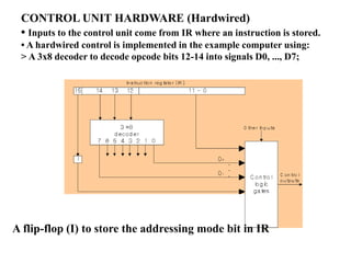
CONTROL UNIT HARDWARE(Hardwired)
• Inputs to the control unit come from IR where an instruction is stored.
• A hardwired control is implemented in the example computer using:
> A 3x8 decoder to decode opcode bits 12-14 into signals D0, ..., D7;
A flip-flop (I) to store the addressing mode bit in IR
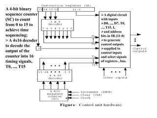
21.
A 4-bit binary
sequencecounter
(SC) to count
from 0 to 15 to
achieve time
sequencing;
> A 4x16 decoder
to decode the
output of the
counter into 16
timing signals,
T0, ..., T15
A digital circuit
with inputs
D0, ..., D7, T0,
..., T15, I,
and address
bits in IR (11-0)
to generate
control outputs
supplied to
control inputs
and select signals
of registers , bus.
22.
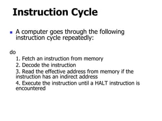
Instruction Cycle
Acomputer goes through the following
instruction cycle repeatedly:
do
1. Fetch an instruction from memory
2. Decode the instruction
3. Read the effective address from memory if the
instruction has an indirect address
4. Execute the instruction until a HALT instruction is
encountered
23.
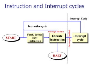
Instruction and Interruptcycles
Fetch, decode
Next
Instruction
Execute
Instruction
START
HALT
Instruction cycle
Interrupt
cycle
Interrupt Cycle
Interrupts
Enabled
Interrupts Disabled
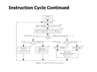
Sequencing the Operations
Step 0: (Initialize)
• Initially, the program counter (PC)
is loaded with the address of the first
instruction in the program.
• The sequence counter (SC) is
initialized to 0, providing a decoded
timing signal T0.
SC ← 0
• After each clock pulse, SC is
incremented by one, so that the
timing signals go through a sequence
T0, T1, T2, and so on.
26.
Fetch Cycle: (Fetchthe Instruction)
Step 1:
During the first time pulse T0, the
instruction address is transferred from the
PC to AR.
Step 2:
During the time pulse T1, the instruction read
from memory is then transferred to the
instruction register IR, and PC is incremented
by 1 for the address of the next instruction in
the program.
The micro operations for fetch cycle:
• T0 : AR ← PC
• T1 : IR ← M[AR], PC ← PC + 1
27.
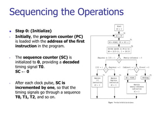
Decode Cycle: (Decodethe Instruction)
Step 3:
At time T2,
• The operation code in IR is decoded.
• The address part of the instruction is
transferred to AR.
• The mode bit (direct/indirect bit) is
transferred to flip-flop I.
The microoperations for decode cycle:
• T2 : D₀, D₁, ... D₇ ← Decode IR (12-14)
• AR ← IR (0-11)
• I ← IR (15) D₀ : 000
D₁ : 001
D₂ : 010
D₃ : 011
D₄ : 100
D₅ : 101
D₆ : 110
D₇ : 111
I Opcode Address
15 14 12 11 0
28.
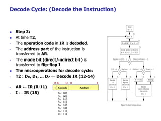
Determine the Typeof Instruction:
(Decision)
Step 4: During time T₃, at this time the type of instruction is determined so
the data preparation and execution of the instruction takes place.
The three possible computer instruction types available in the basic
computers are:
•Memory-reference instructions
•Register-reference instructions, or
•Input-output instructions
Instruction Formats
Memory-Reference Instructions (OP-code = 000 ~ 110)
Register-Reference Instructions (OP-code = 111, I = 0)
Input-Output Instructions (OP-code = 111, I = 1)
29.
Determine the Typeof Instruction:
•Decoder output D₇ is equal to 1, if the operation code is
equal to 111.
•Decoder output D₇ is equal to 0, if the operation code is one
of the other seven values 000 through 110.
• If D₇ = 1, the instruction must be a register-reference or
input-output type.
• If D₇ = 0, the instruction must be a memory-reference.
Control then inspects the value of the first bit of the
instruction, which is in flip-flop I.
• If D₇ = 0 and I = 1, it is a memory reference
instruction with an indirect address.
• It is then necessary to read the effective address
from memory. (Operand Fetch)
• T₃ : AR ← M[AR]
• If D₇ = 0 and I = 0, it is a memory reference
instruction with a direct address.
• It is not necessary to do anything since the effective
address is already in AR.
• T₃ : Nothing
• If D₇ = 1 and I = 1, it is an input-output instruction.
• If D₇ = 1 and I = 0, it is a register-reference
instruction.
30.
Execute the Instruction:
•A register-reference or input-output instruction can
be executed with the clock timing signal T₃.
• T₃ : Execute a register-reference instruction
• T₃ : Execute an input-output instruction
• After the instruction is executed, SC is cleared to 0 and
control returns to the fetch phase with T₀ = 1.
• A memory reference instruction can be executed with
the clock timing signal T₄.
• T₄ : Execute a memory-reference instruction
• After the instruction is executed, SC is cleared to 0 and
control returns to the fetch phase with T₀ = 1.
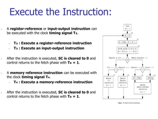
REGISTER-REFERENCE INSTRUCTIONS
• The12 register-reference instructions are recognized by I = 0
and D7 = 1 (IR(12-14) = 111). Each operation is designated by
the presence of 1 in one of the bits in IR(0-11). Therefore D7I`T3
r = 1 is common to all register-transfer instructions.
33.
Memory Reference
Instructions
Sincethe data stored in memory cannot be
processed directly (the memory unit is not
connected to the ALU), the actual execution in
the bus system require a sequence of
microoperations.
(Note that T0-T2 for fetch an instruction; T3 for
AR M[AR] if indirect memory addressing.
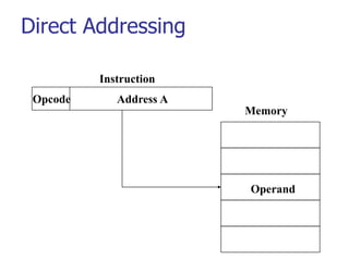
Direct Addressing
Thevalue of address field is
the address of the operand
Notation:
If X is an address then (X)
denotes the value contained
in the memory cell with
address X
EA = Effective Address in
memory of the operand
EA = A
e.g. ADD 457
Look in memory at address
457 for operand
Add contents to accumulator:
AC+M[457]AC
Or AC+(457)->AC
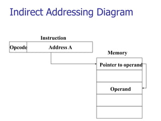
Indirect Addressing (1)
The memory cell referenced by the
address field contains the address of
(i.e., the pointer to) the operand
If A is the value of the address field,
then EA=(A)
e.g.
Above control word signifies 1 as indirect
addressing and operand part is containing
address and tells to look at address 300,
then go to address 1350 and look there for
operand
Add to accumulator the content of the
cell pointed to by the content of
Acc+M[1350]Acc
1 Add 300

![Single Accumulator Organization
All the operations on a system are performed with an
implied accumulator register. The instruction format in
this type of computer uses one address field.
For example, the instruction for arithmetic addition is
defined by an assembly language instruction ‘ADD.’
Where X is the operand’s address, the ADD instruction
results in the operation.
AC ← AC + M[X].
AC is the accumulator register, M[X] symbolizes the
memory word located at address X.](https://image.slidesharecdn.com/1-250225180344-6db5387b/85/Instruction-execution-cycle-_-11-320.jpg)
![General Register Organization
The general register type computers employ two or
three address fields in their instruction format. Each
address field specifies a processor register or a memory.
An instruction symbolized by ADD R1, X specifies the
operation R1 ← R + M [X].
This instruction has two address fields: register R1 and
memory address X.](https://image.slidesharecdn.com/1-250225180344-6db5387b/85/Instruction-execution-cycle-_-12-320.jpg)
![Fetch Cycle: (Fetch the Instruction)
Step 1:
During the first time pulse T0, the
instruction address is transferred from the
PC to AR.
Step 2:
During the time pulse T1, the instruction read
from memory is then transferred to the
instruction register IR, and PC is incremented
by 1 for the address of the next instruction in
the program.
The micro operations for fetch cycle:
• T0 : AR ← PC
• T1 : IR ← M[AR], PC ← PC + 1](https://image.slidesharecdn.com/1-250225180344-6db5387b/85/Instruction-execution-cycle-_-26-320.jpg)
![Determine the Type of Instruction:
•Decoder output D₇ is equal to 1, if the operation code is
equal to 111.
•Decoder output D₇ is equal to 0, if the operation code is one
of the other seven values 000 through 110.
• If D₇ = 1, the instruction must be a register-reference or
input-output type.
• If D₇ = 0, the instruction must be a memory-reference.
Control then inspects the value of the first bit of the
instruction, which is in flip-flop I.
• If D₇ = 0 and I = 1, it is a memory reference
instruction with an indirect address.
• It is then necessary to read the effective address
from memory. (Operand Fetch)
• T₃ : AR ← M[AR]
• If D₇ = 0 and I = 0, it is a memory reference
instruction with a direct address.
• It is not necessary to do anything since the effective
address is already in AR.
• T₃ : Nothing
• If D₇ = 1 and I = 1, it is an input-output instruction.
• If D₇ = 1 and I = 0, it is a register-reference
instruction.](https://image.slidesharecdn.com/1-250225180344-6db5387b/85/Instruction-execution-cycle-_-29-320.jpg)
![Memory Reference
Instructions
Since the data stored in memory cannot be
processed directly (the memory unit is not
connected to the ALU), the actual execution in
the bus system require a sequence of
microoperations.
(Note that T0-T2 for fetch an instruction; T3 for
AR M[AR] if indirect memory addressing.](https://image.slidesharecdn.com/1-250225180344-6db5387b/85/Instruction-execution-cycle-_-33-320.jpg)
![Direct Addressing
The value of address field is
the address of the operand
Notation:
If X is an address then (X)
denotes the value contained
in the memory cell with
address X
EA = Effective Address in
memory of the operand
EA = A
e.g. ADD 457
Look in memory at address
457 for operand
Add contents to accumulator:
AC+M[457]AC
Or AC+(457)->AC](https://image.slidesharecdn.com/1-250225180344-6db5387b/85/Instruction-execution-cycle-_-35-320.jpg)
![Indirect Addressing (1)
The memory cell referenced by the
address field contains the address of
(i.e., the pointer to) the operand
If A is the value of the address field,
then EA=(A)
e.g.
Above control word signifies 1 as indirect
addressing and operand part is containing
address and tells to look at address 300,
then go to address 1350 and look there for
operand
Add to accumulator the content of the
cell pointed to by the content of
Acc+M[1350]Acc
1 Add 300](https://image.slidesharecdn.com/1-250225180344-6db5387b/85/Instruction-execution-cycle-_-37-320.jpg)