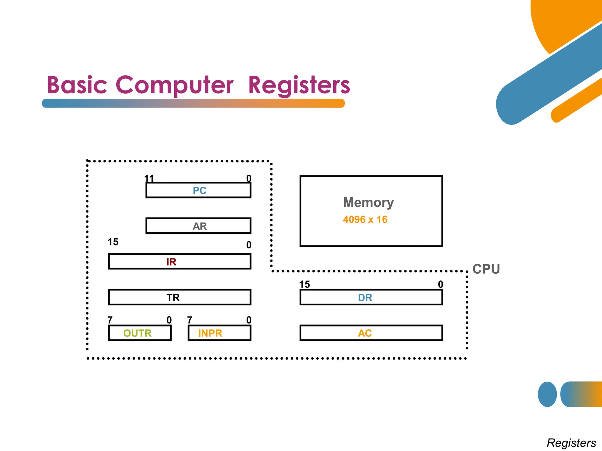
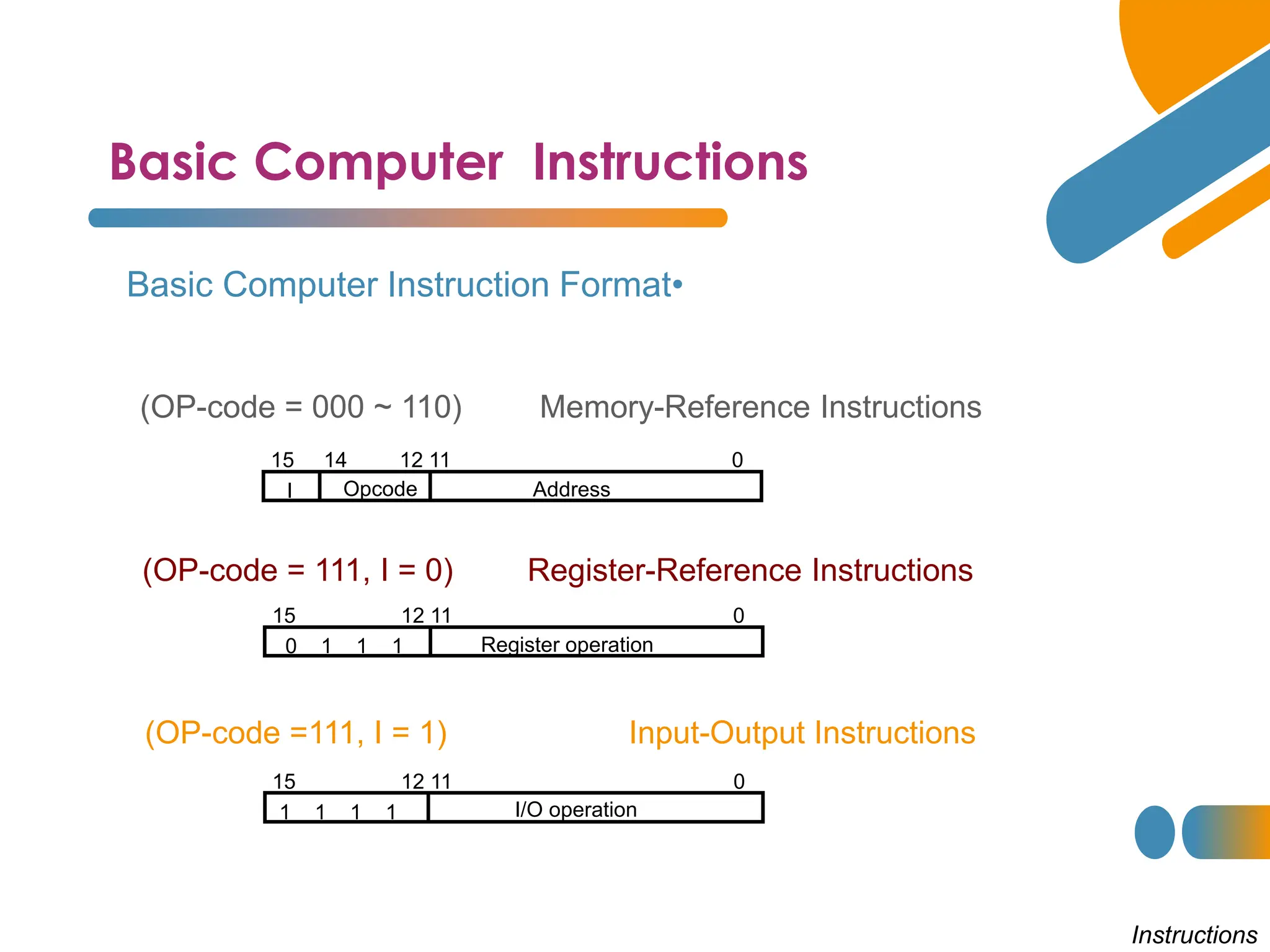
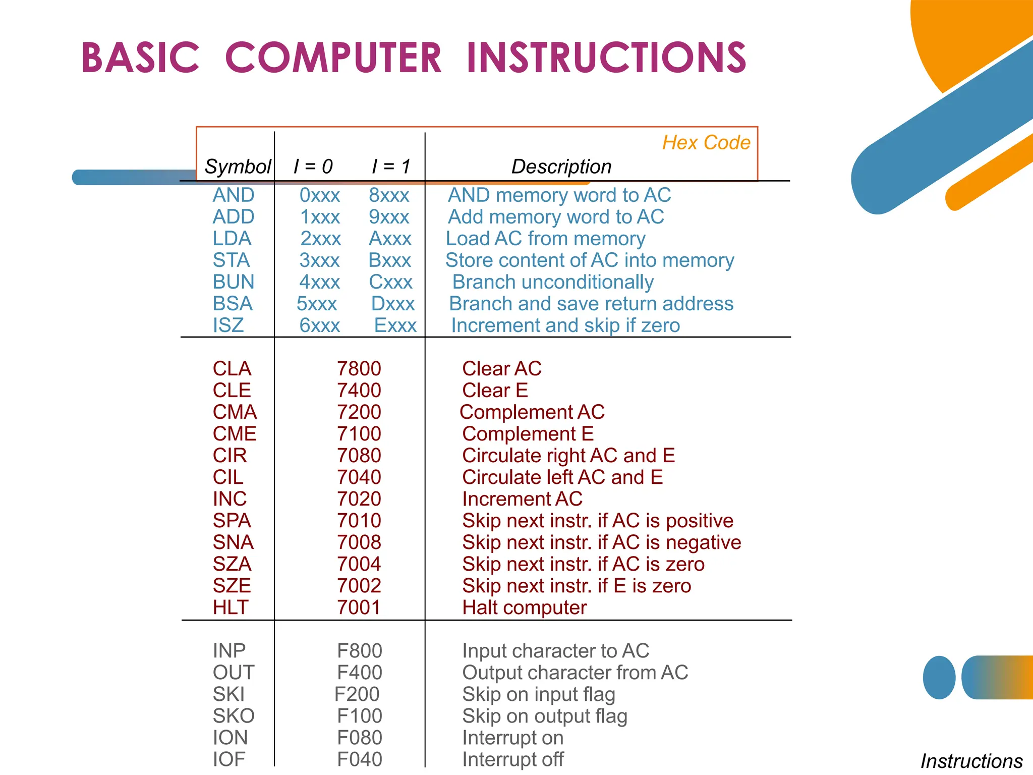
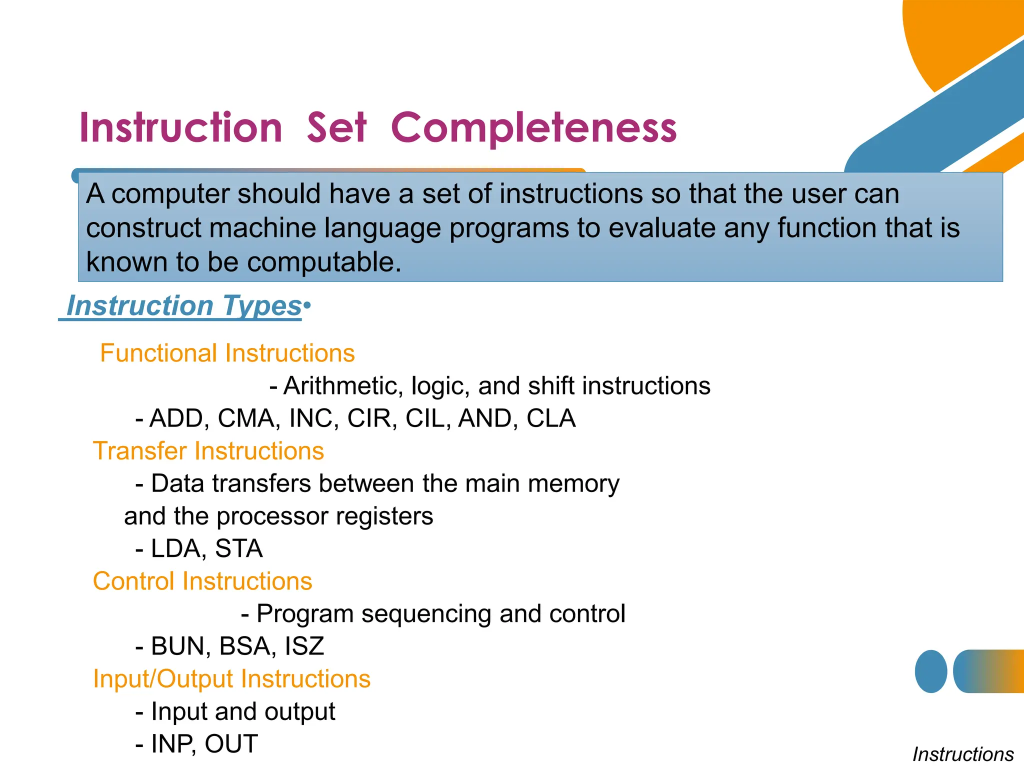
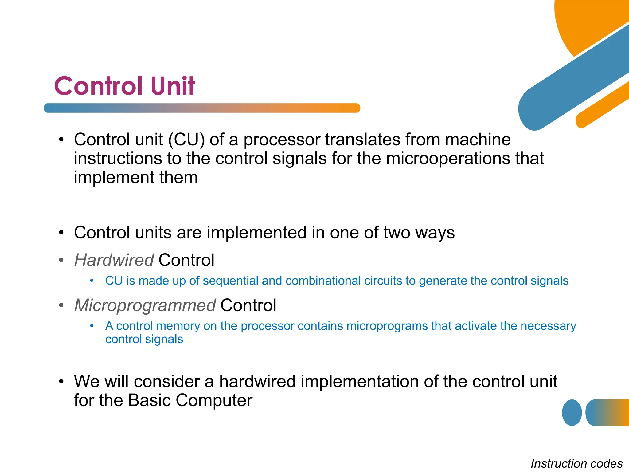
The document provides a detailed overview of basic computer organization and design, focusing on instruction codes, processor registers, and the instruction cycle. It explains the components of a basic computer system, including the processor, memory, instruction formats, and the control unit's functionality. Furthermore, it outlines various addressing modes, operations, and the significance of different registers used in the execution of instructions.

![Fetch and Decode
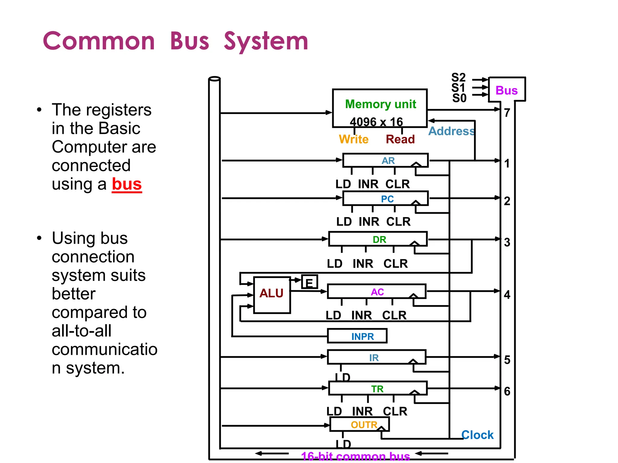
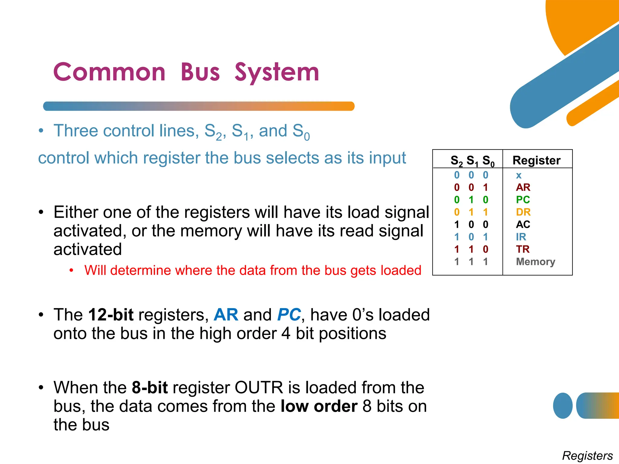
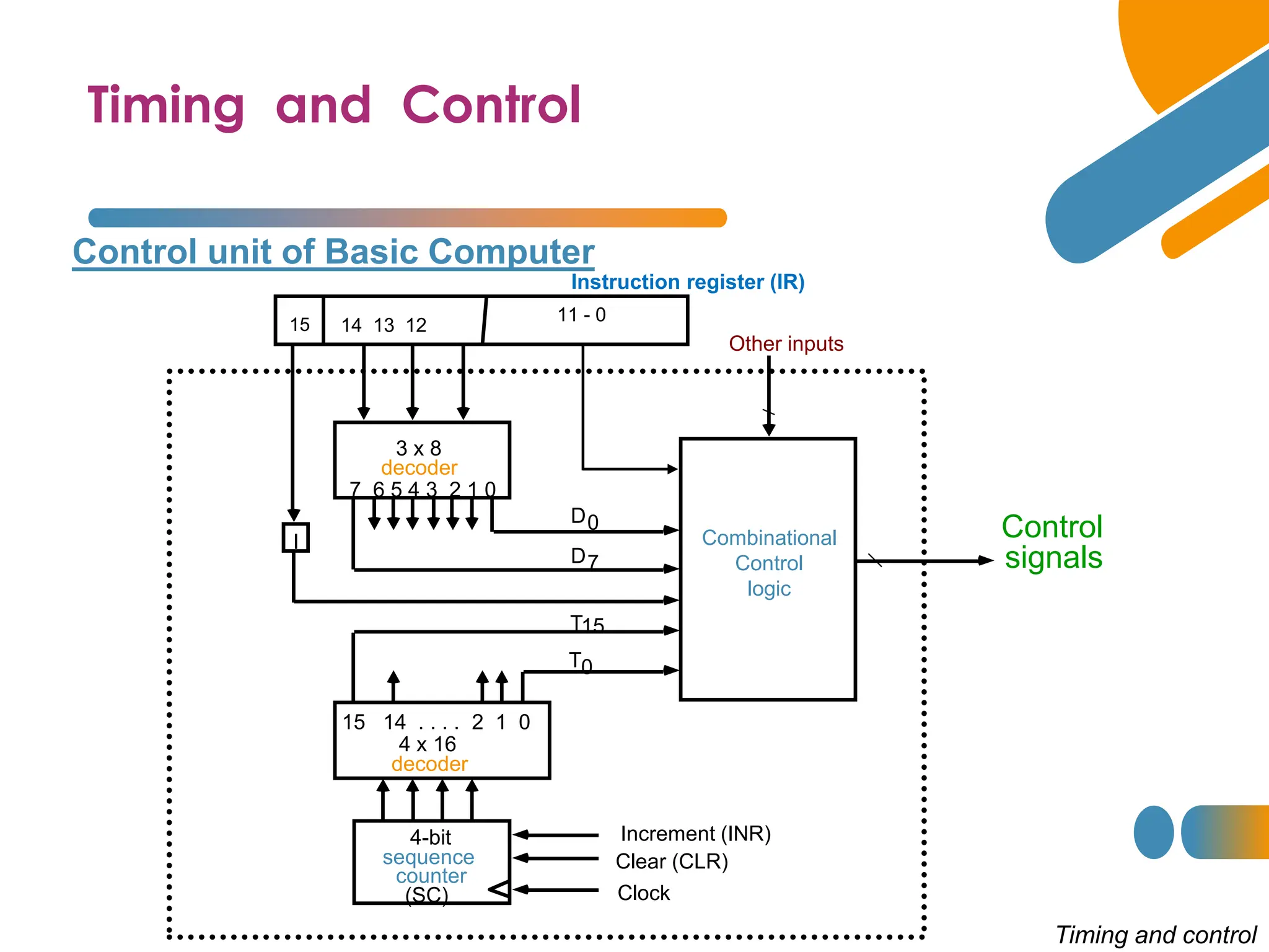
Fetch and Decode T0: AR PC (S0S1S2=010, T0=1)
S2
S1
S0
Bus
7
Memory
unit
Address
Read
AR
LD
PC
INR
IR
LD Clock
1
2
5
Common bus
T1
T0
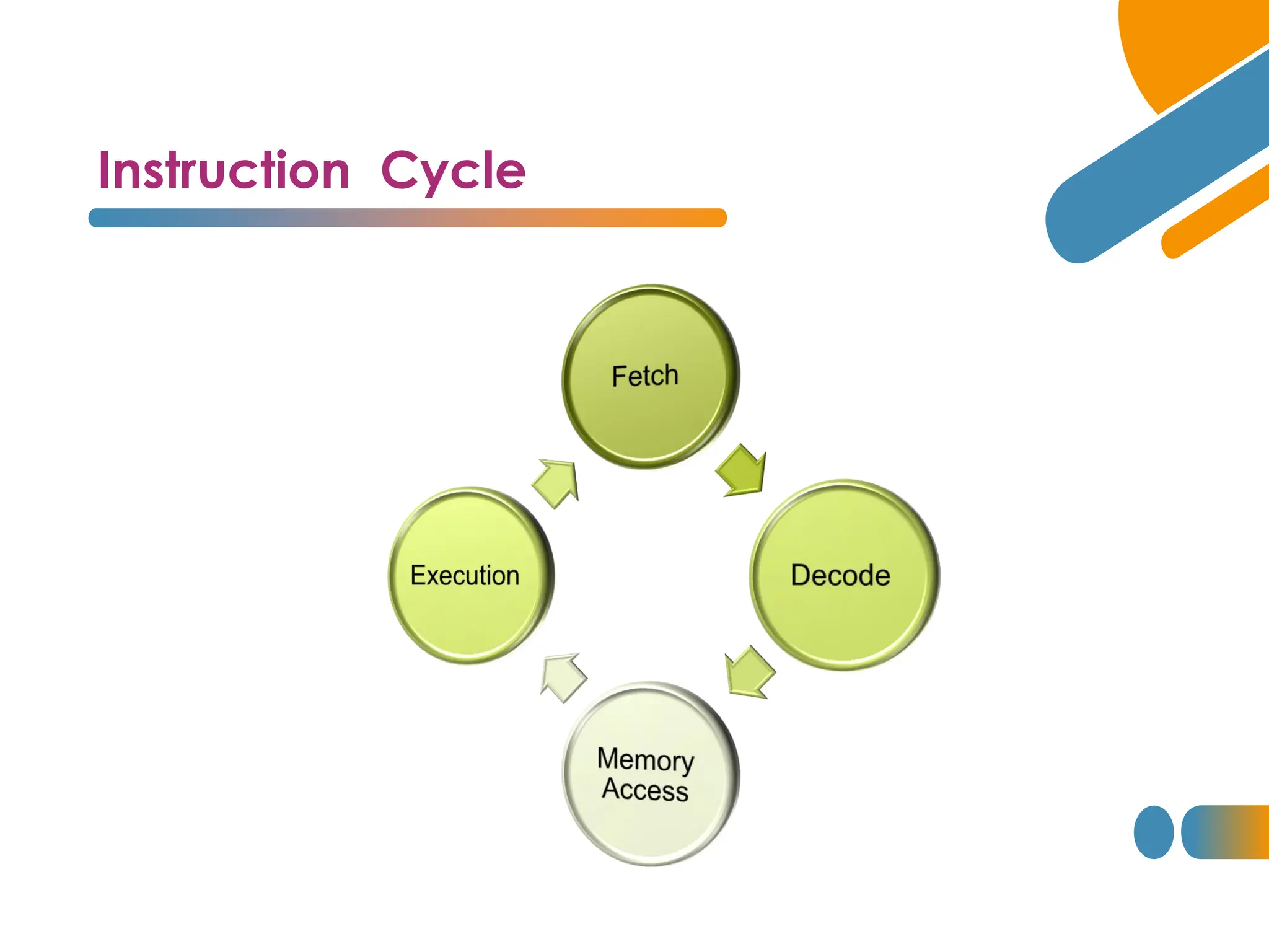
Instruction Cycle
T1: IR M [AR], PC PC + 1 (S0S1S2=111, T1=1)
T2: D0, . . . , D7 Decode IR(12-14),
AR IR(0-11),
I IR(15)](https://image.slidesharecdn.com/2024lecture6come321-241127085611-51f87175/75/2024_lecture6_come321-pdf-25-2048.jpg)
![Determine The Type of Instruction
= 0 (direct)
Start
SC 0
AR PC T0
IR M[AR], PC PC + 1 T1
AR IR(0-11), I IR(15)
Decode Opcode in IR(12-14),
T2
D7
= 0 (Memory-reference)
(Register or I/O) = 1
I
I
Execute
register-reference
instruction
SC 0
Execute
input-output
instruction
SC 0
M[AR]
AR Nothing
= 0 (register)
(I/O) = 1 (indirect) = 1
T3 T3 T3
T3
Execute
memory-reference
instruction
SC 0
T4
D'7IT3: AR M[AR]
D'7I'T3: Nothing
D7I'T3: Execute a register-reference instr.
D7IT3: Execute an input-output instr.](https://image.slidesharecdn.com/2024lecture6come321-241127085611-51f87175/75/2024_lecture6_come321-pdf-26-2048.jpg)