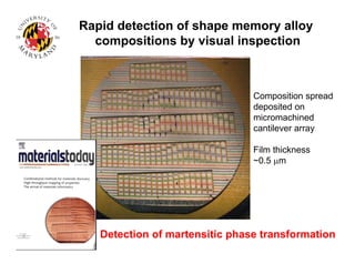
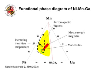
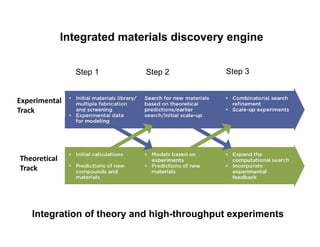
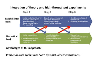
Downloaded 35 times


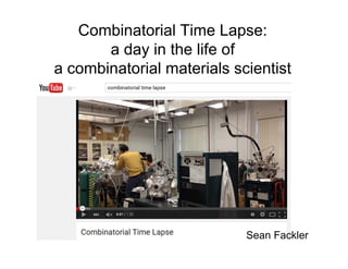
![Mode/materials
[reference]
Physical parameter/
phenomenon
Spatial
resolution
Dielectric [12-14] Complex dielectric
constant
100 nm
Metal [13] Impedance/resistivity 100 nm
Non-linear
dielectric [15,18]
Non-linear dielectric
constant
1 nm
FMR Ferromagnetic
resonance
100 nm*
STM-ESR Electron
spin resonance
Atomic
resolution
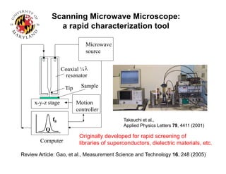
Capabilities of Multiscale Microwave Microscope
Mapping of various physical properties can be obtained
at macroscopic scale (~ 1 cm) down to the listed spatial resolution](https://image.slidesharecdn.com/takeuchiplenary2compatibilitymode-151002203614-lva1-app6892/85/Combinatorial-approach-to-materials-discovery-30-320.jpg)
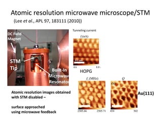
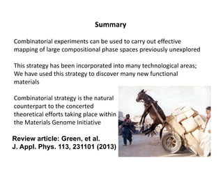
![FeBx: we have found the superconductor
Susceptibility
shows diamagnetism
Bc2(T)= Bc2(0)[1-(T/Tc)2]/ [1+(T/Tc)2]
gives Bc2(0) = 2 T
-> Type II BCS superconductor
Partial R drop
~ 10 K?
Superconducting phase was detected in 2 spread wafers](https://image.slidesharecdn.com/takeuchiplenary2compatibilitymode-151002203614-lva1-app6892/85/Combinatorial-approach-to-materials-discovery-60-320.jpg)
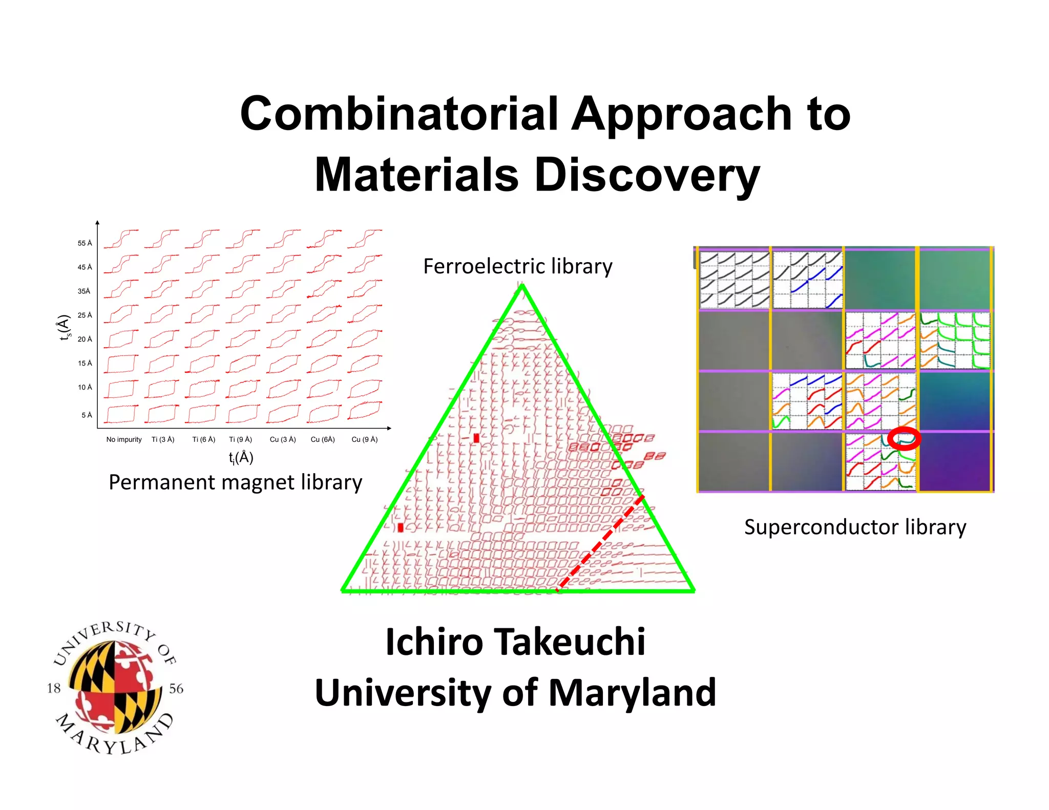
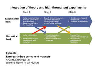
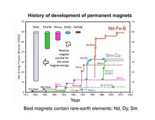
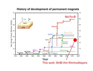
The document discusses a combinatorial approach to materials discovery, focusing on the development and characterization of various inorganic materials, including permanent magnets and superconductors. It highlights the integration of high-throughput experimental methods with theoretical models to explore large compositional phase spaces and to identify new materials with desired properties. The advancements include techniques for library fabrication, rapid characterization tools, and examples of successful material searches, particularly for rare-earth-free permanent magnets.


![[S.L._Kakani]_Material_Science_(New_Age_Pub.,_2006(BookSee.org).pdf](https://cdn.slidesharecdn.com/ss_thumbnails/s-230301071329-4f25d7e9-thumbnail.jpg?width=640&height=640&fit=bounds)