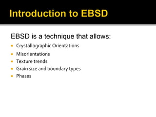
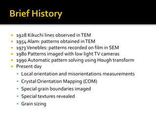
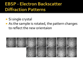
2. Introduction to EBSD
Brief History
Principal system components
How the Pattern is Formed?
EBSP - Electron Backscatter Diffraction
Patterns
Operating conditions
Uses of EBSD
Summary
3. EBSD is a technique that allows:
Crystallographic Orientations
Misorientations
Texture trends
Grain size and boundary types
Phases
4. 1928 Kikuchi lines observed inTEM
1954 Alam: patterns obtained inTEM
1973Venebles: patterns recorded on film in SEM
1980 Patterns imaged with low lightTV cameras
1990 Automatic pattern solving using Hough transform
Present day
Local orientation and misorientations measurements
Crystal Orientation Mapping (COM)
Special grain boundaries imaged
Special textures revealed
Grain sizing
5. Sample tilted at 70° from the horizontal.
A phosphor screen.
A sensitive CCD video camera
A vacuum interface for mounting the phosphor and
camera in an SEM port.
Electronic hardware that controls the SEM, including
the beam position, stage, focus, and magnification.
A computer to control EBSD experiments, analyze the
EBSD pattern and process and display the results.
6.
7. High energy electrons are elastically
scattered by atomic planes in a
crystallographic sample.
8. Accelerating Voltage : 15-30 kV
Beam current : 1-15 nA
Collection angle : 70°
Working distance : 10-25 mm
9. Si single crystal
As the sample is rotated, the pattern changes
to reflect the new orientaion
11. EBSD has become a well established micro structural
analytical technique.
EBSD mapping can be used to explore the processing
microstructure – properties relationships.
EBSD can be used on most crystalline materials
Grain size, sample tilt, and sample preparation are the
primary limitations of the technique.