Downloaded 135 times
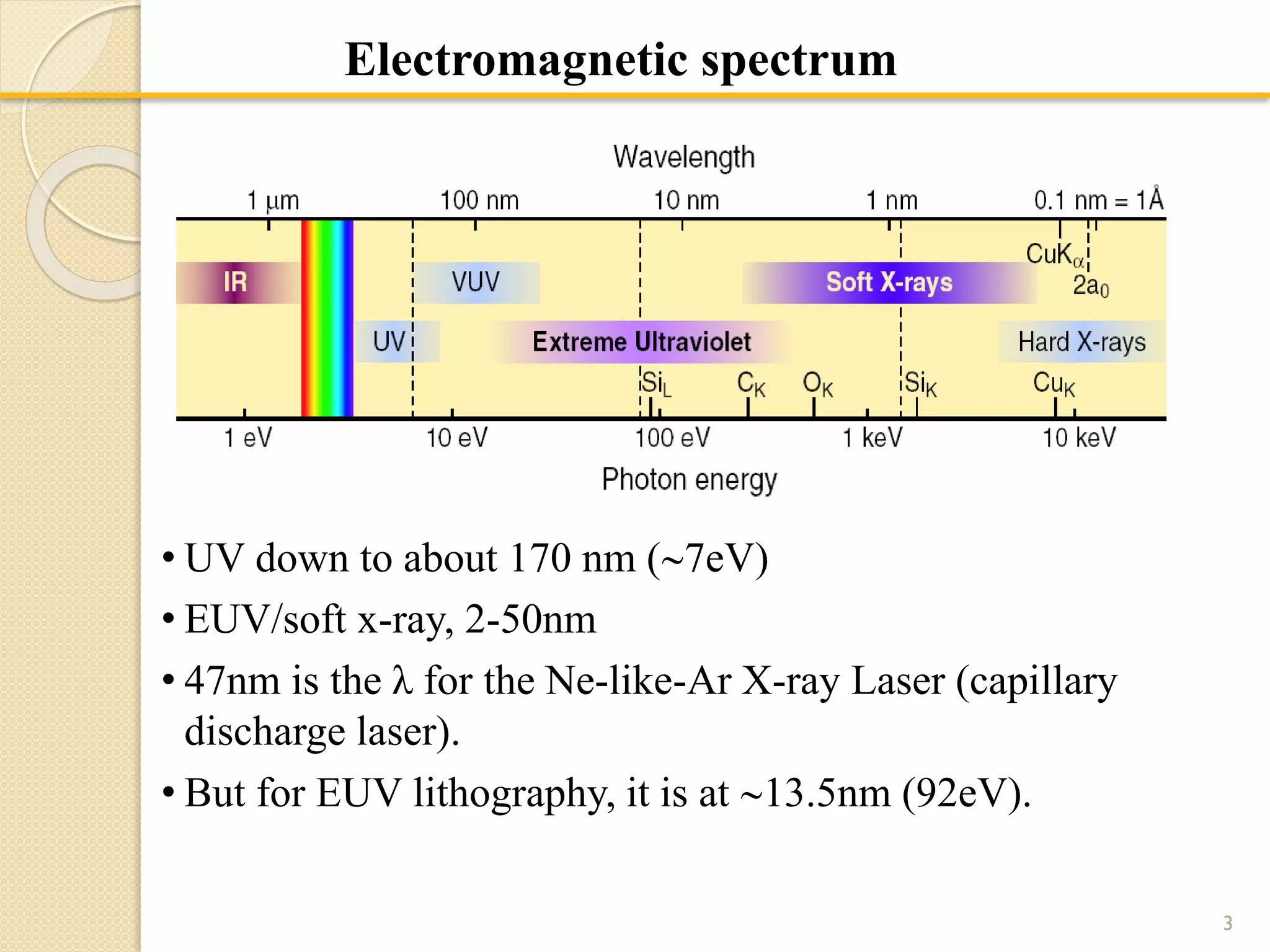


Extreme UV (EUV) lithography uses light with a wavelength of 13.5nm to enable the next generation of smaller computer chips. It relies on specialized curved mirrors coated with molybdenum and silicon instead of lenses, since materials absorb EUV light. The only viable source of 13.5nm light is a hot plasma created by firing a powerful laser at a target. EUV lithography requires operating in a vacuum and developing new resist materials since existing ones strongly absorb the short wavelength light. It holds the potential to further advance computer processing power through smaller transistor sizes.


