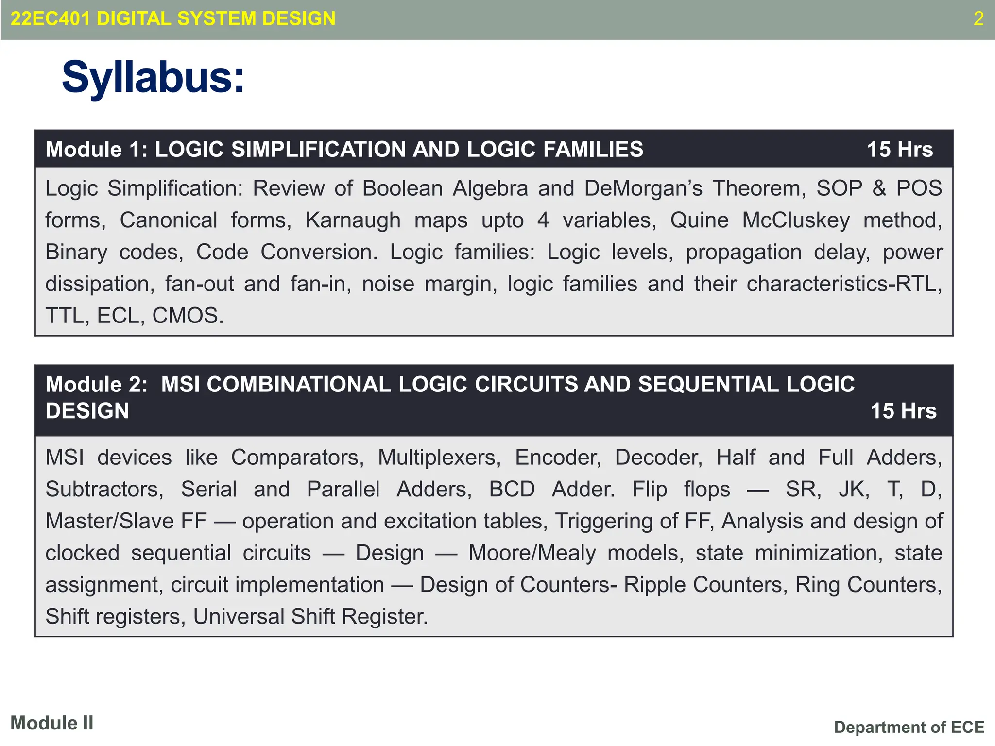
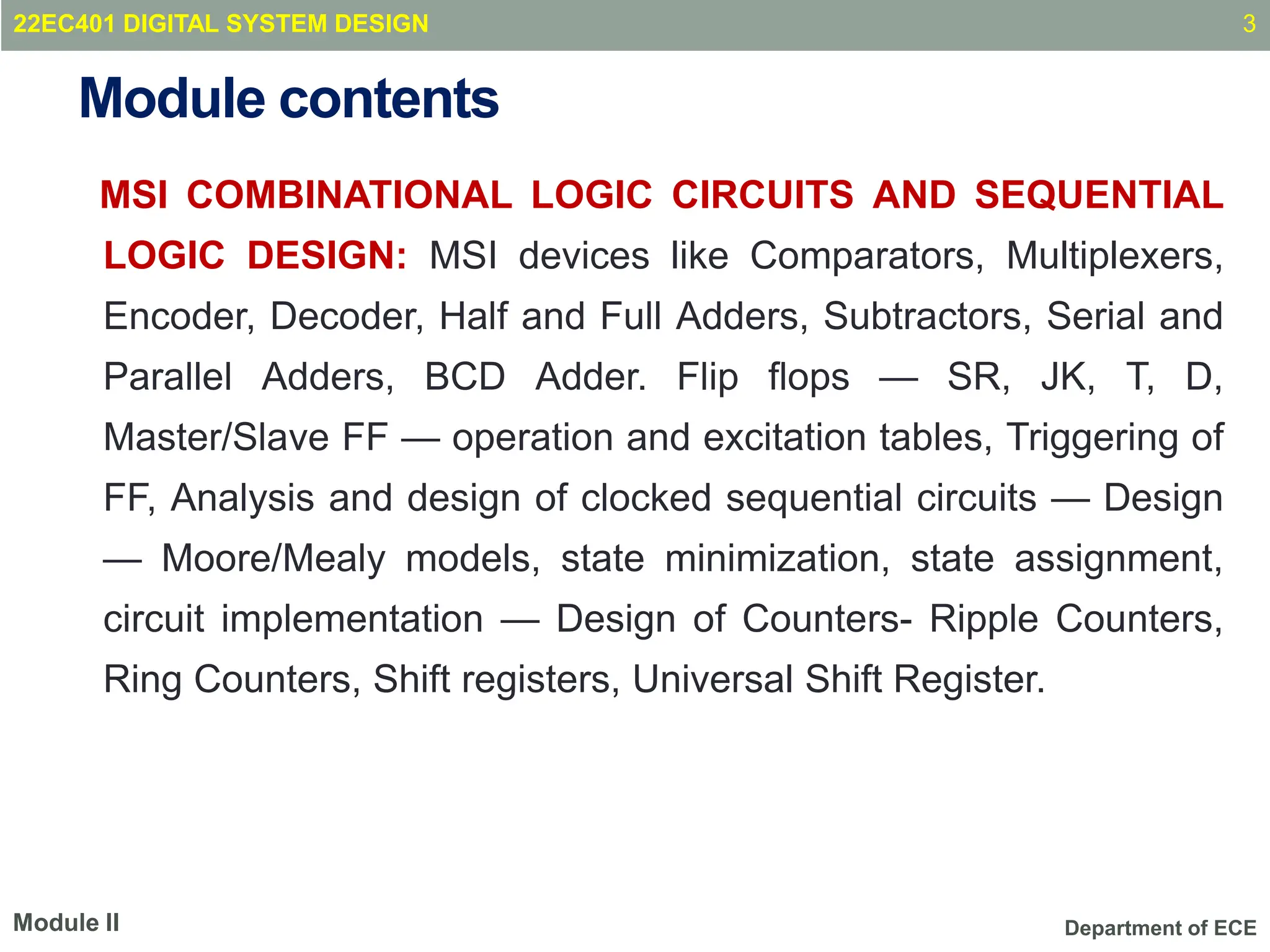
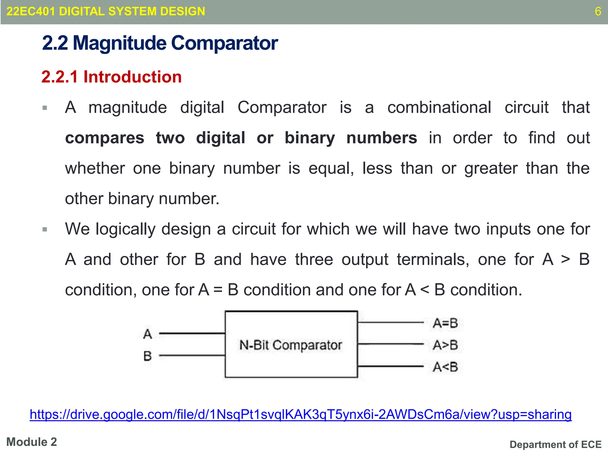
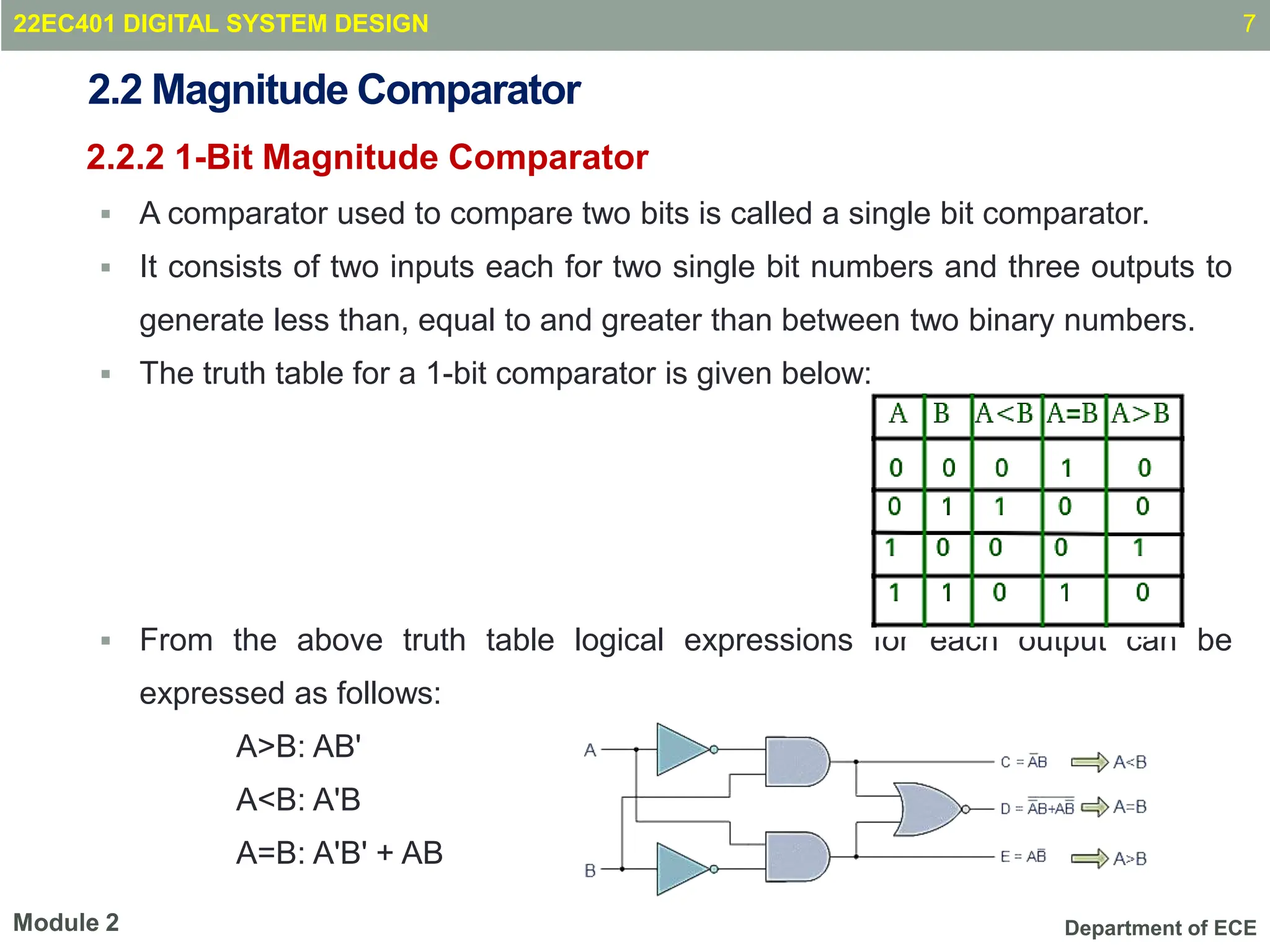
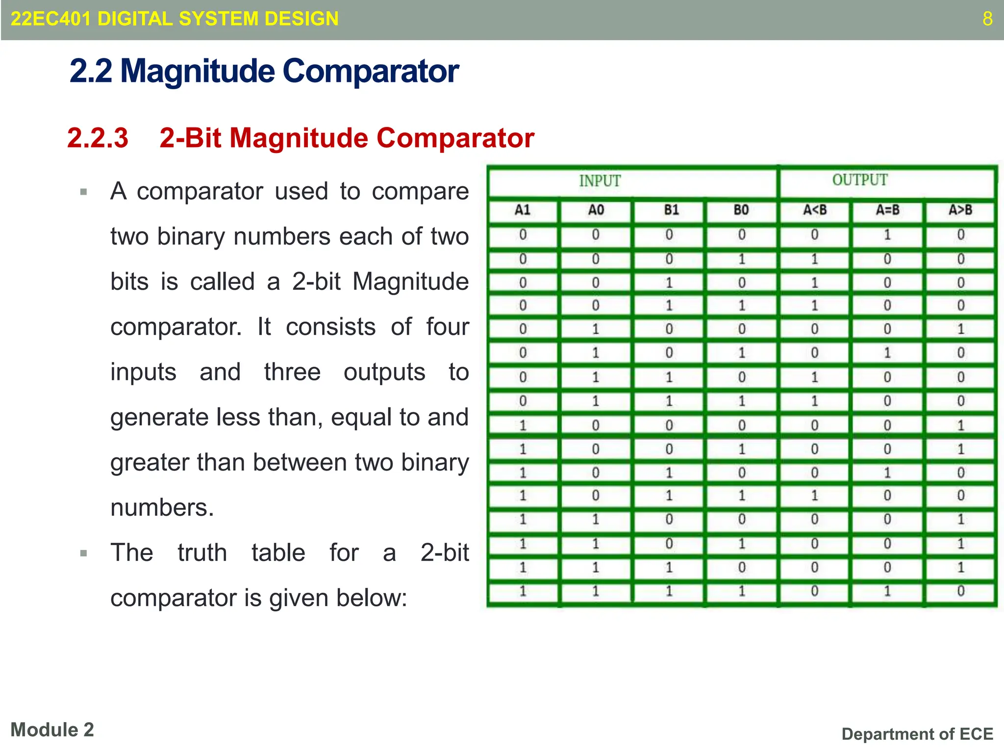
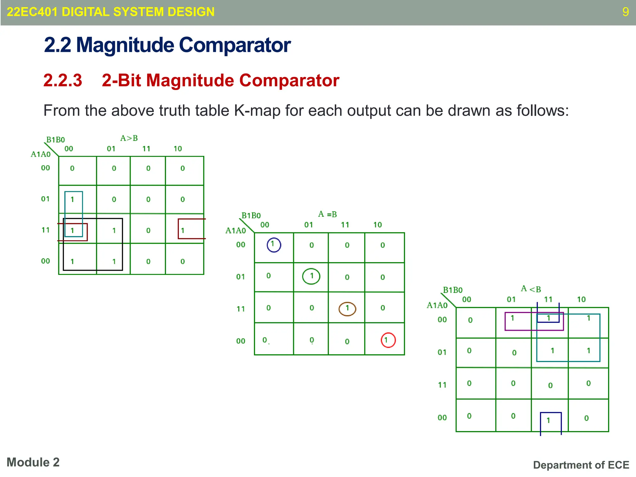
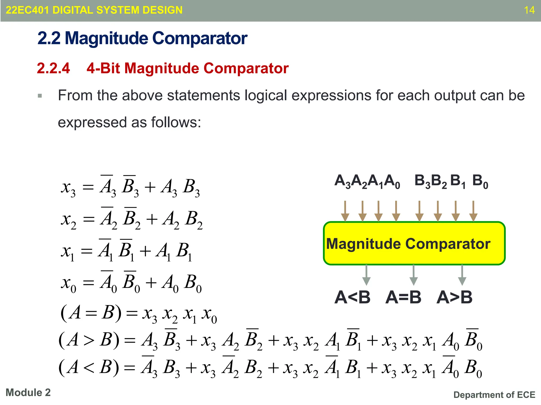
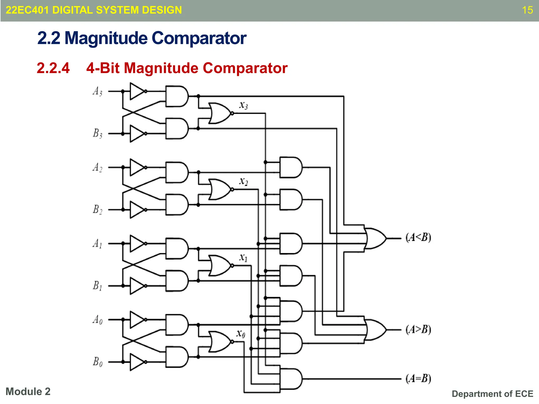
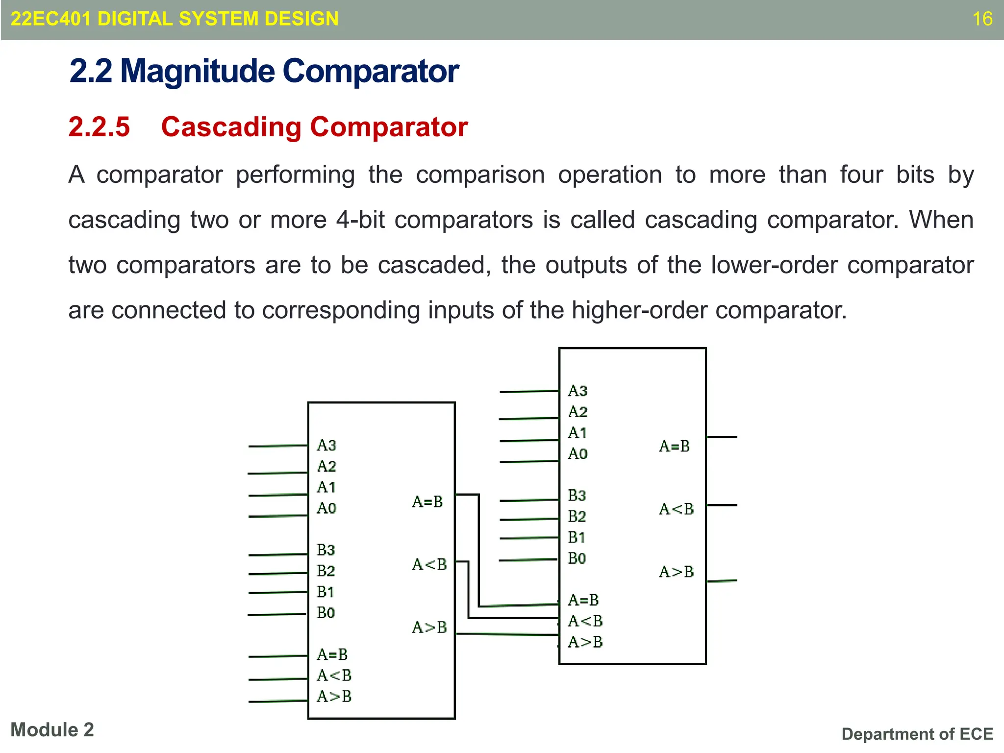
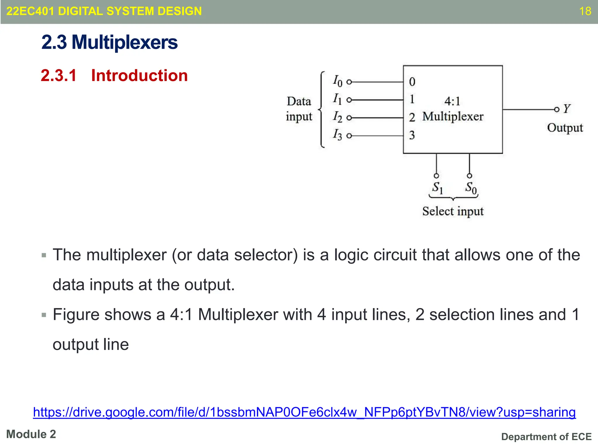
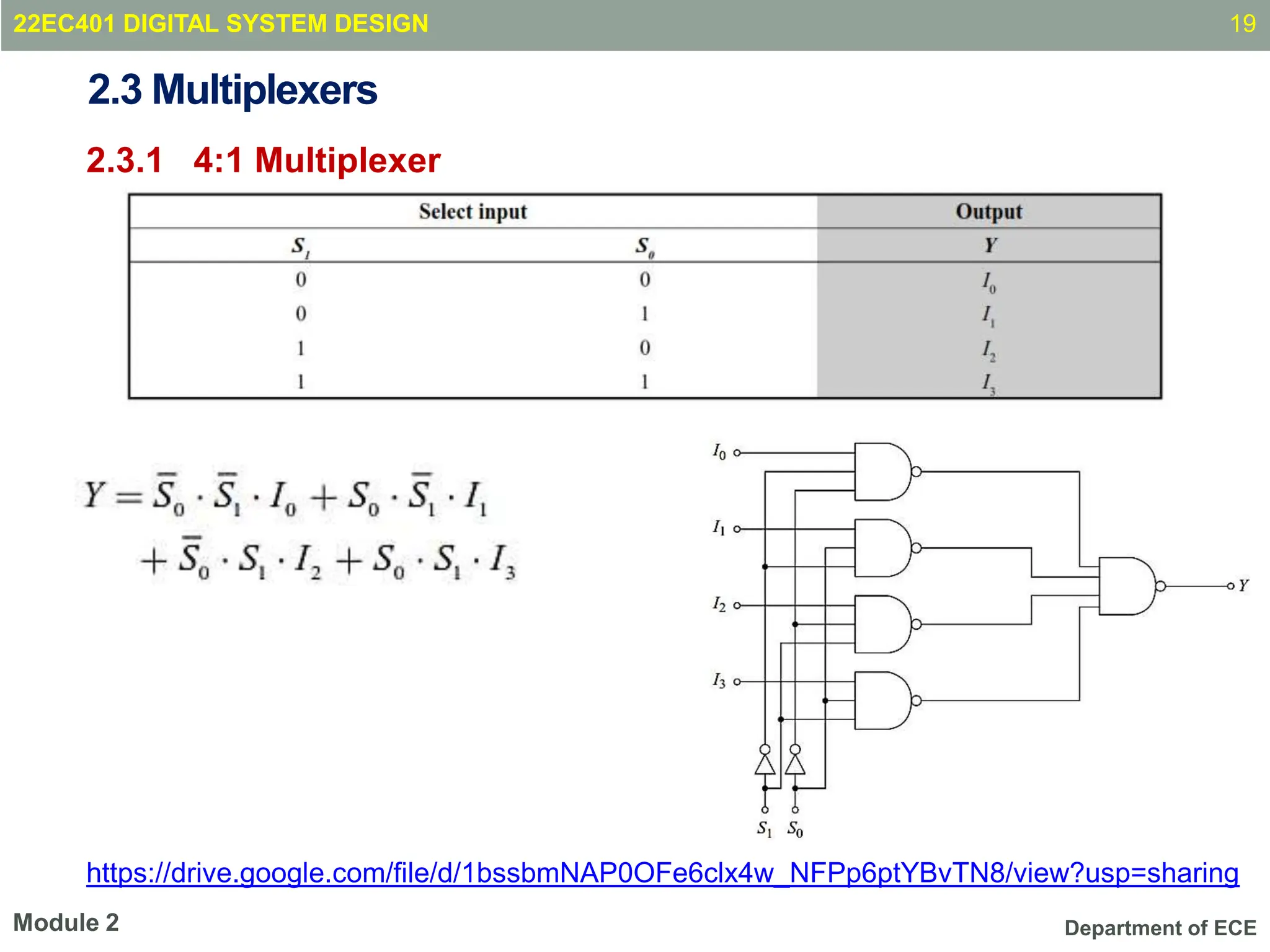
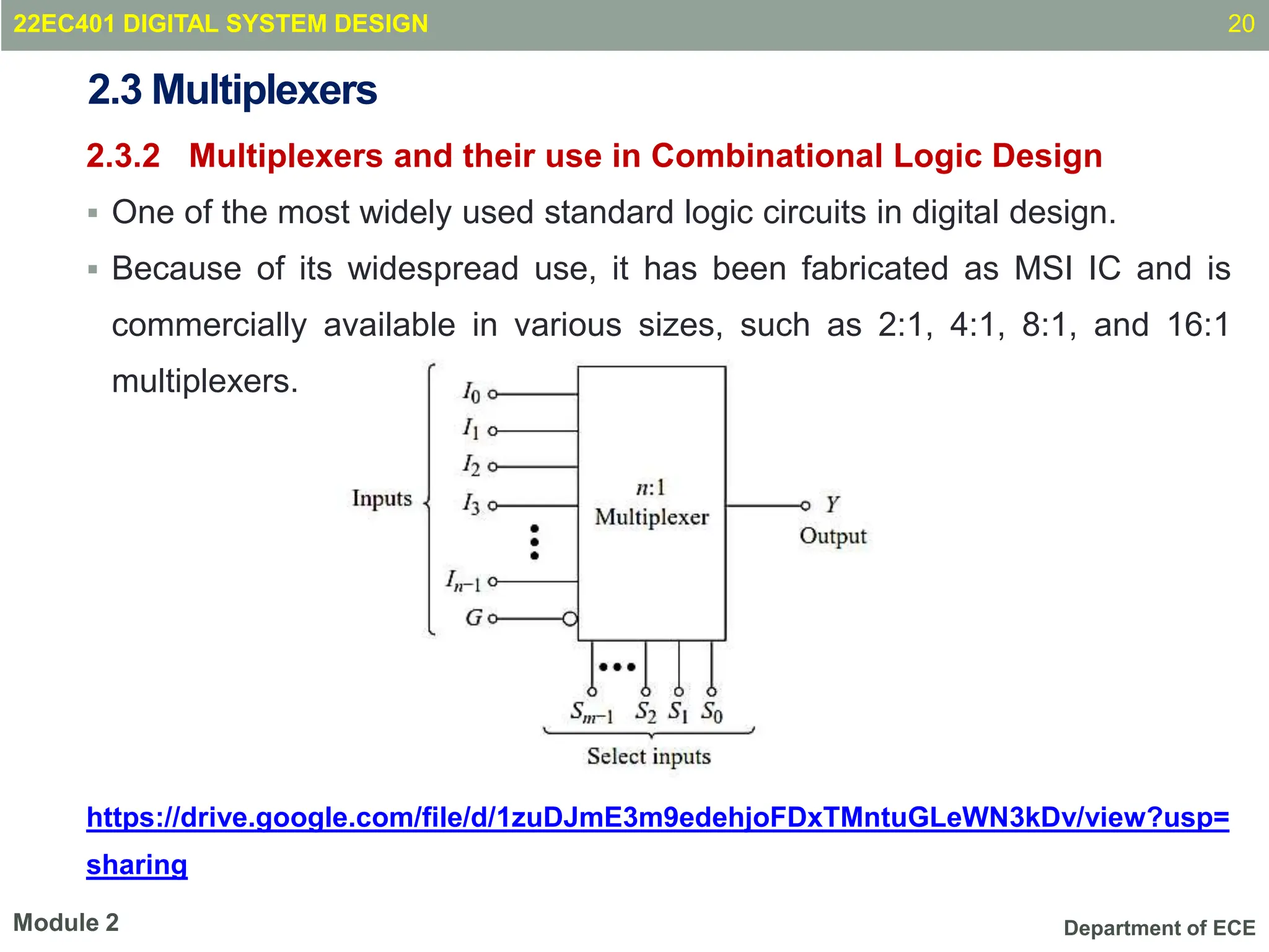
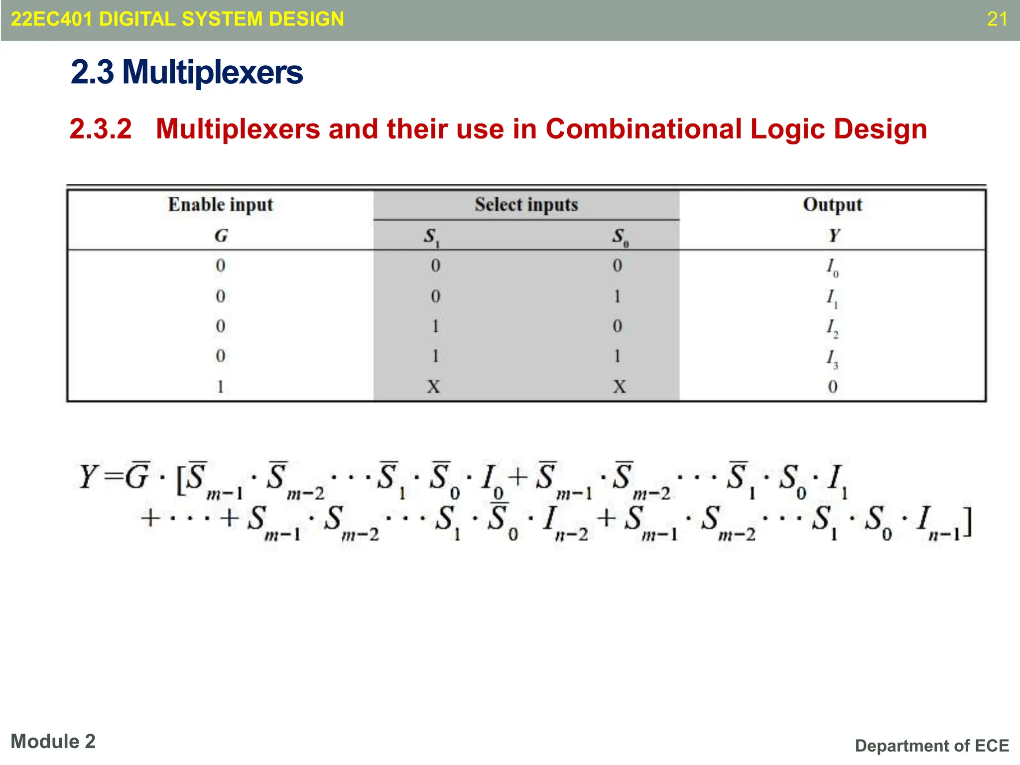
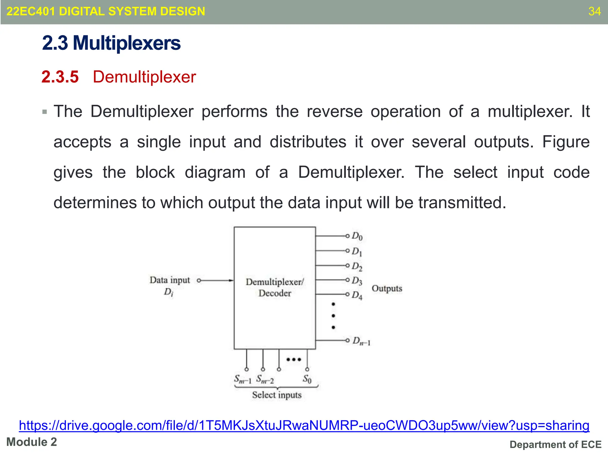
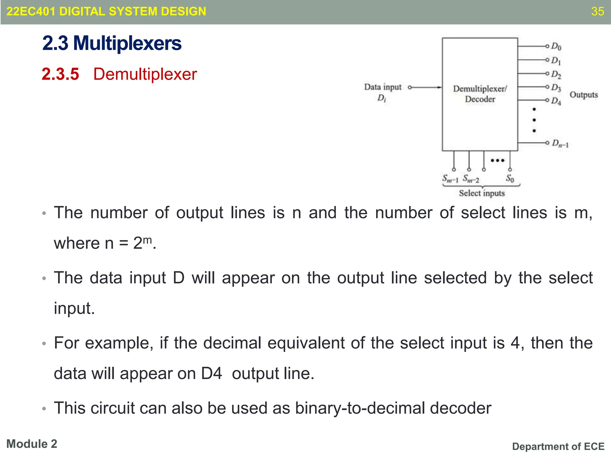
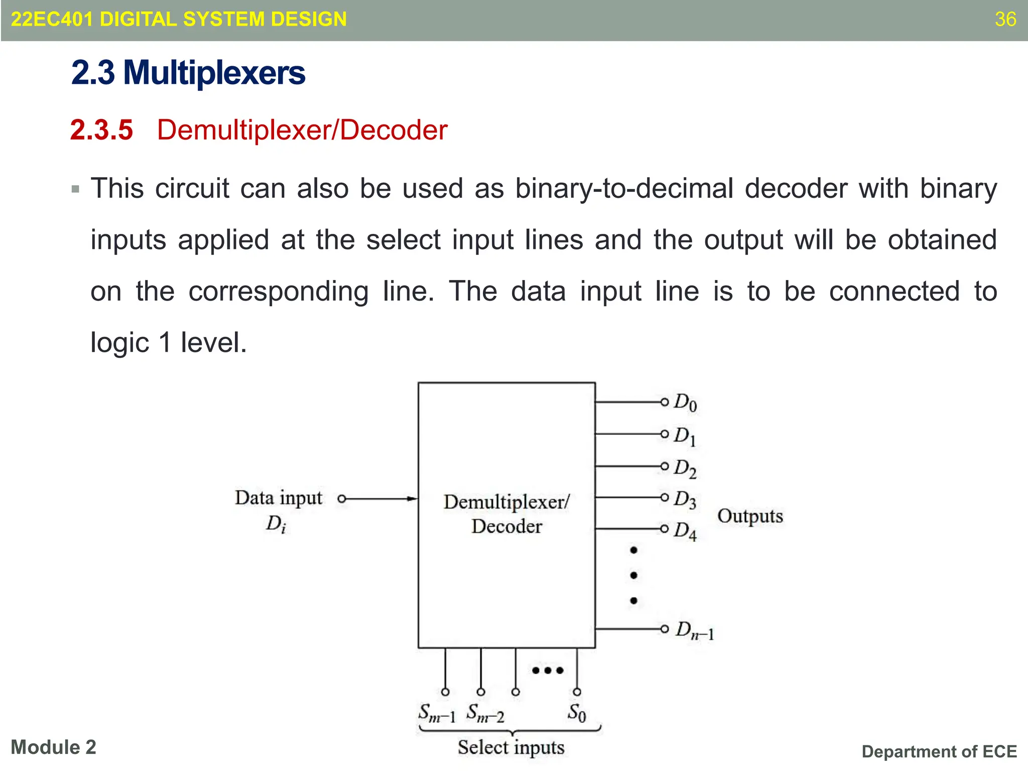
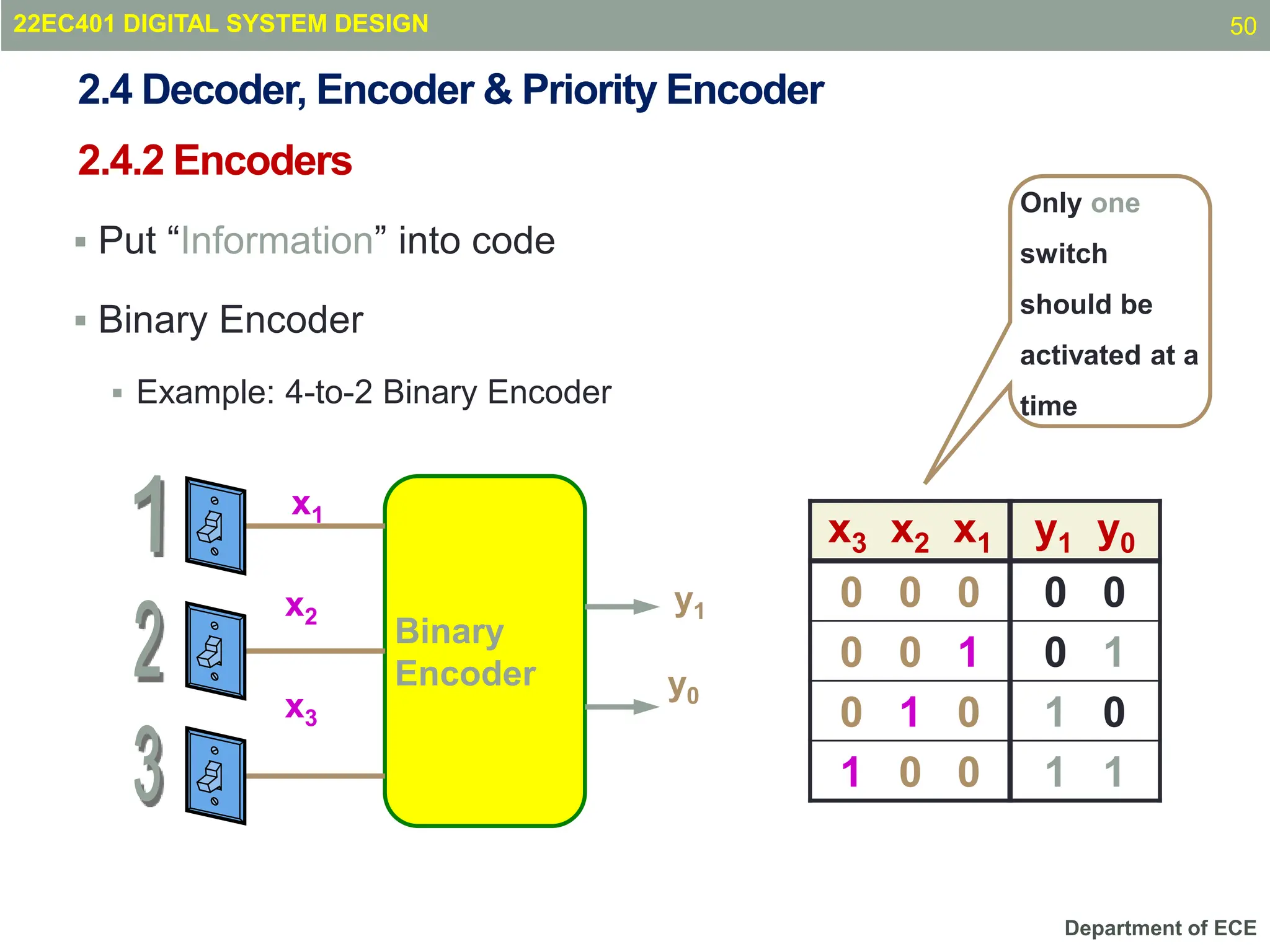
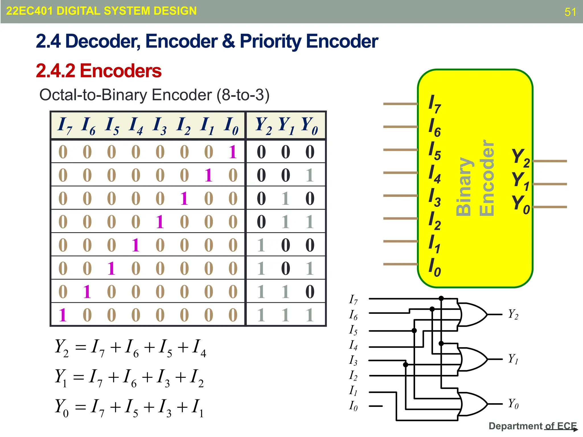
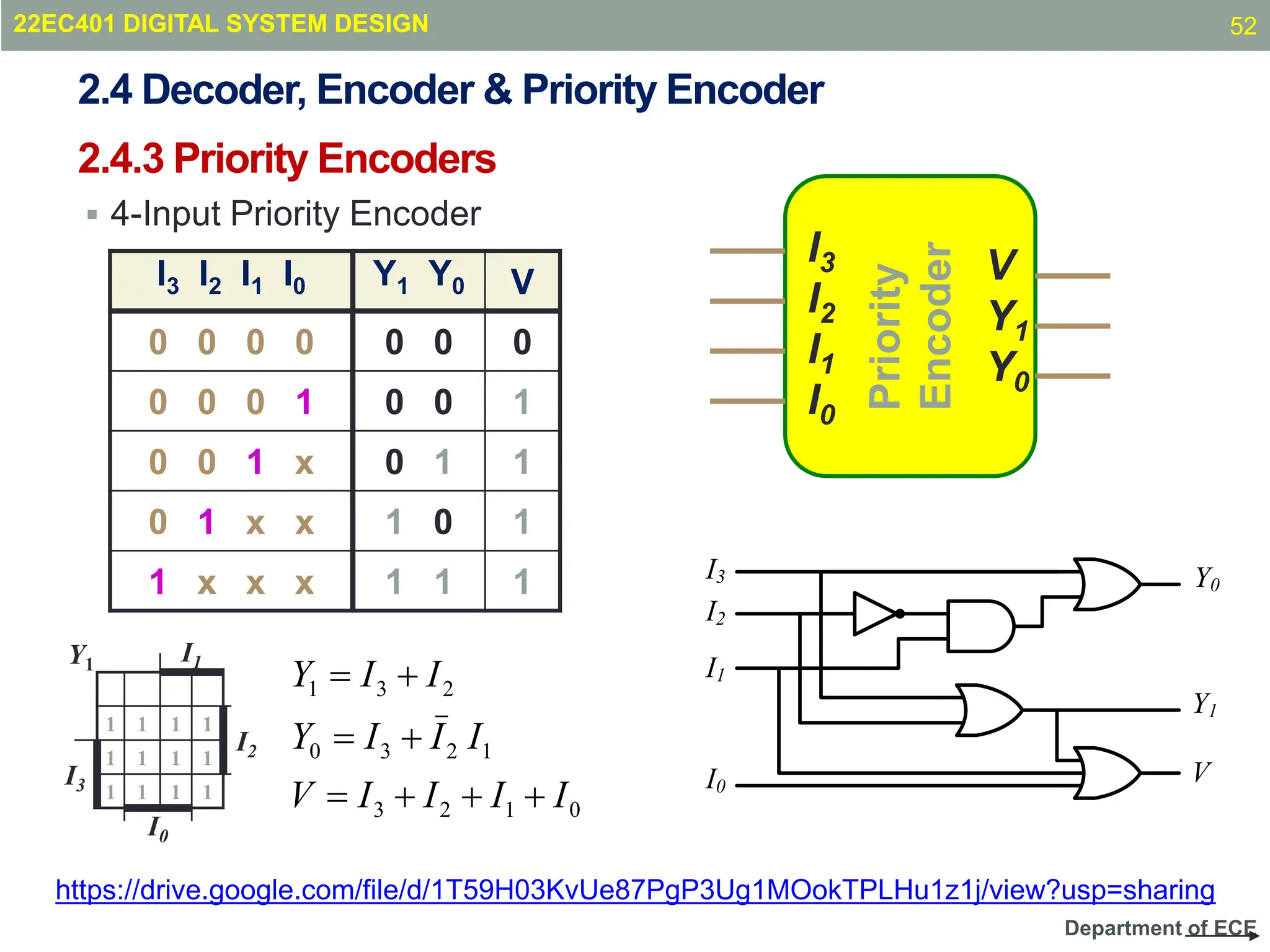
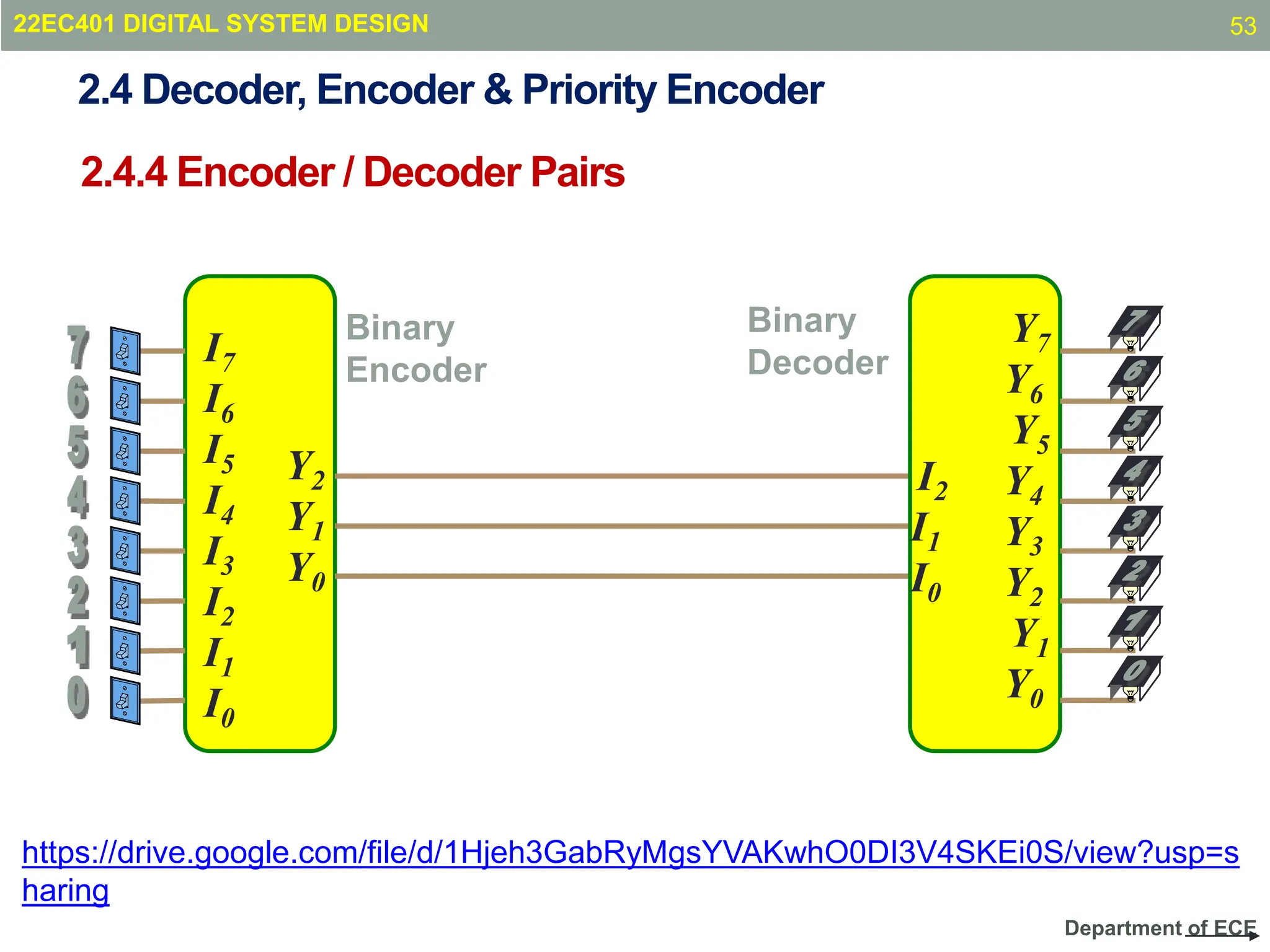
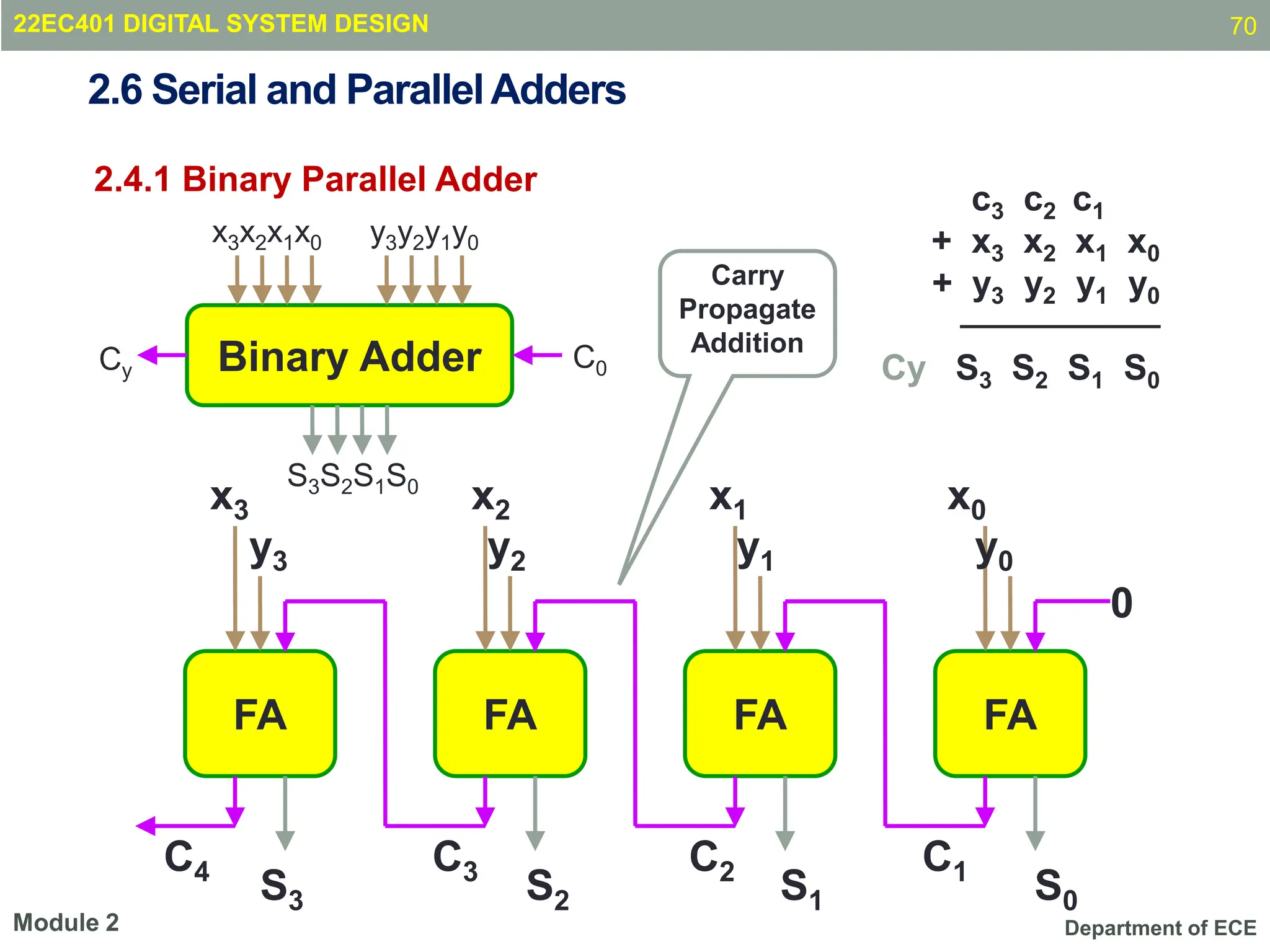
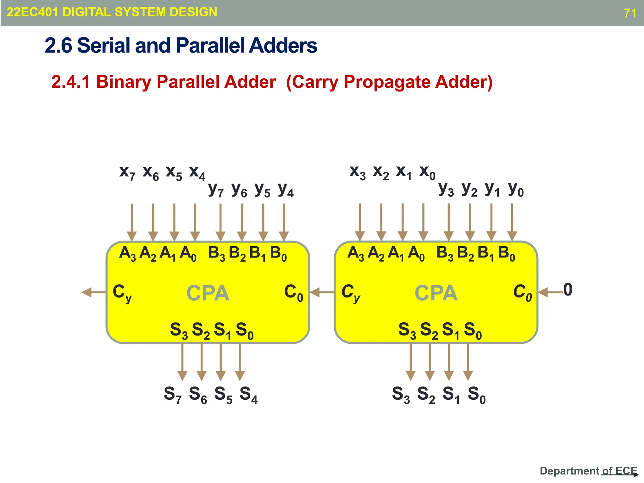
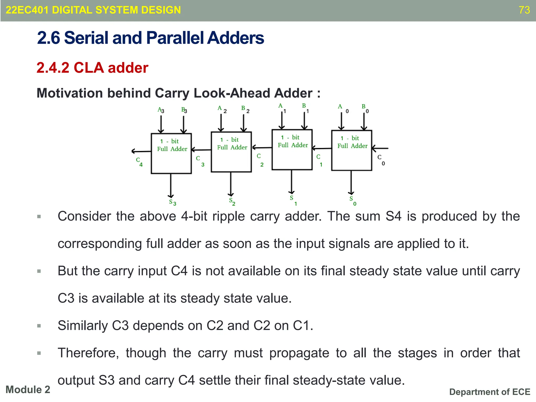
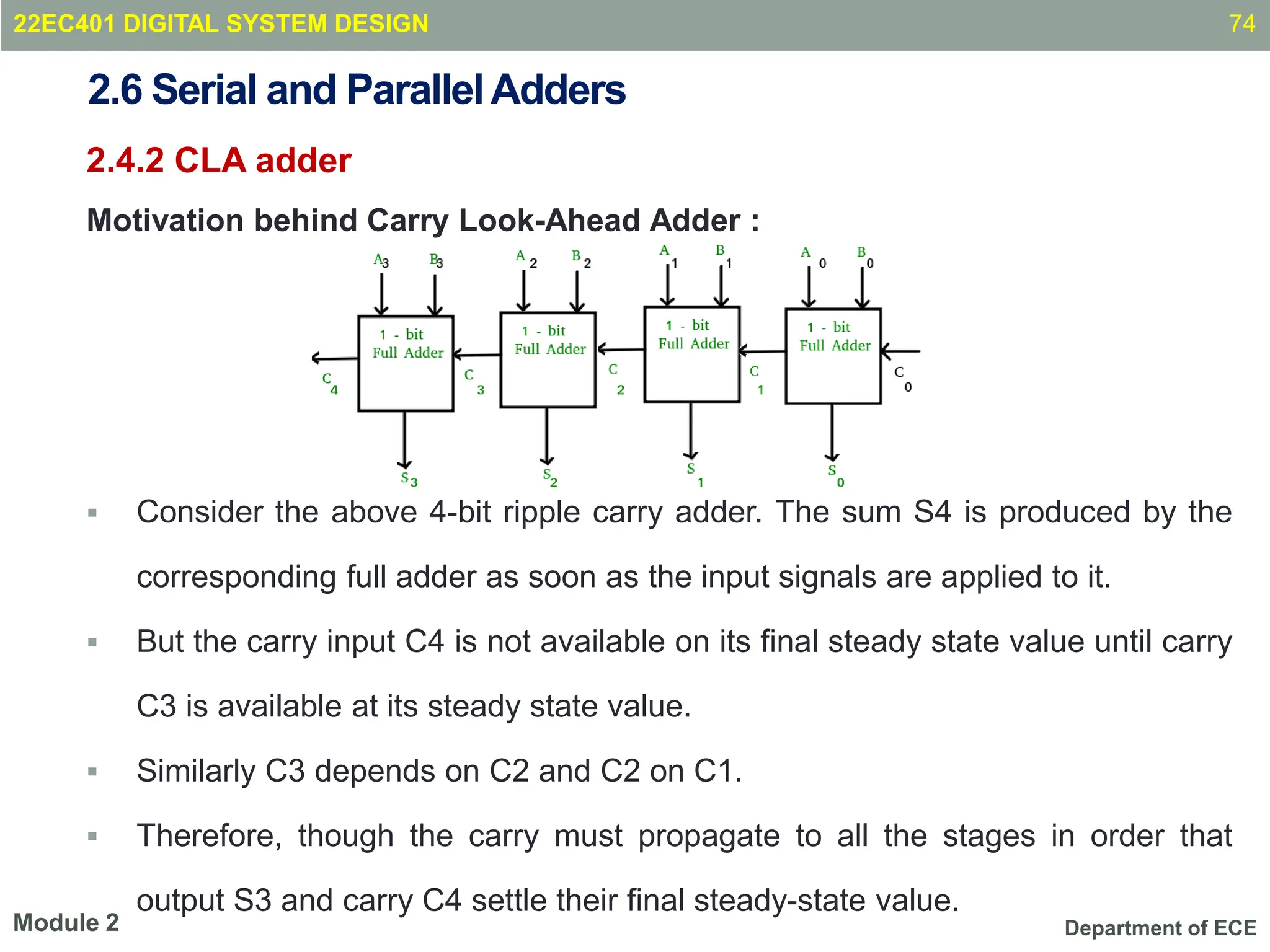
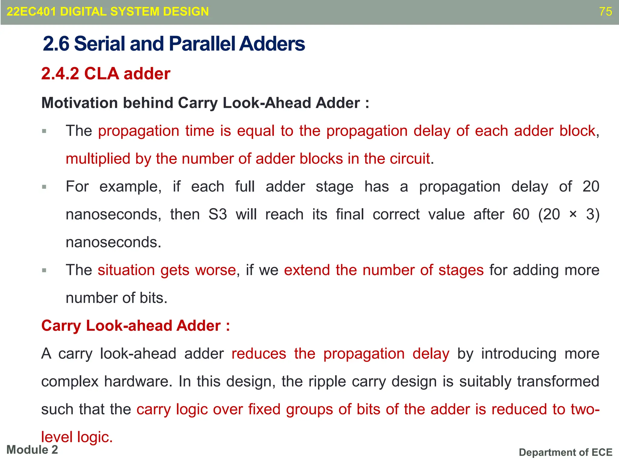
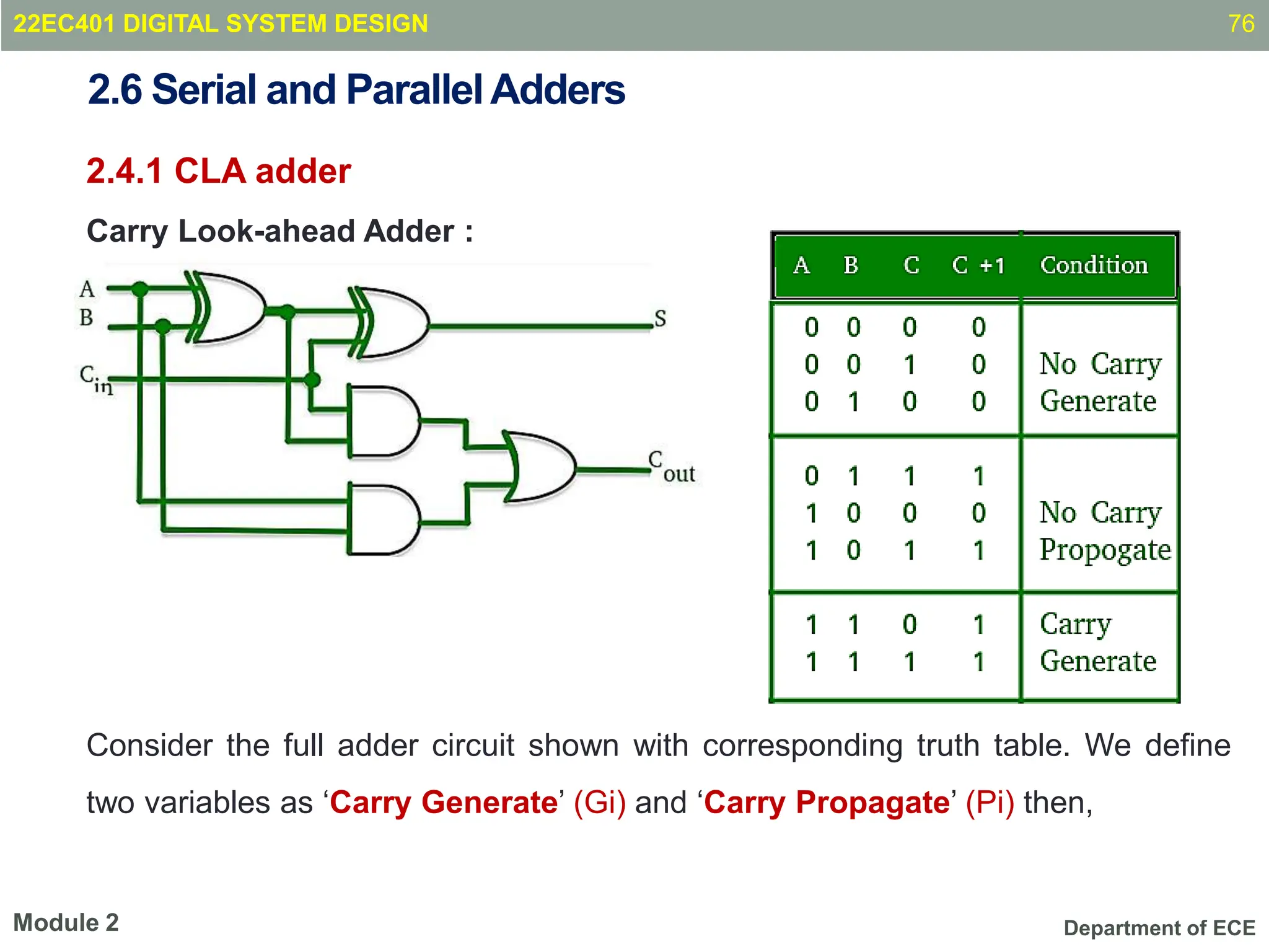
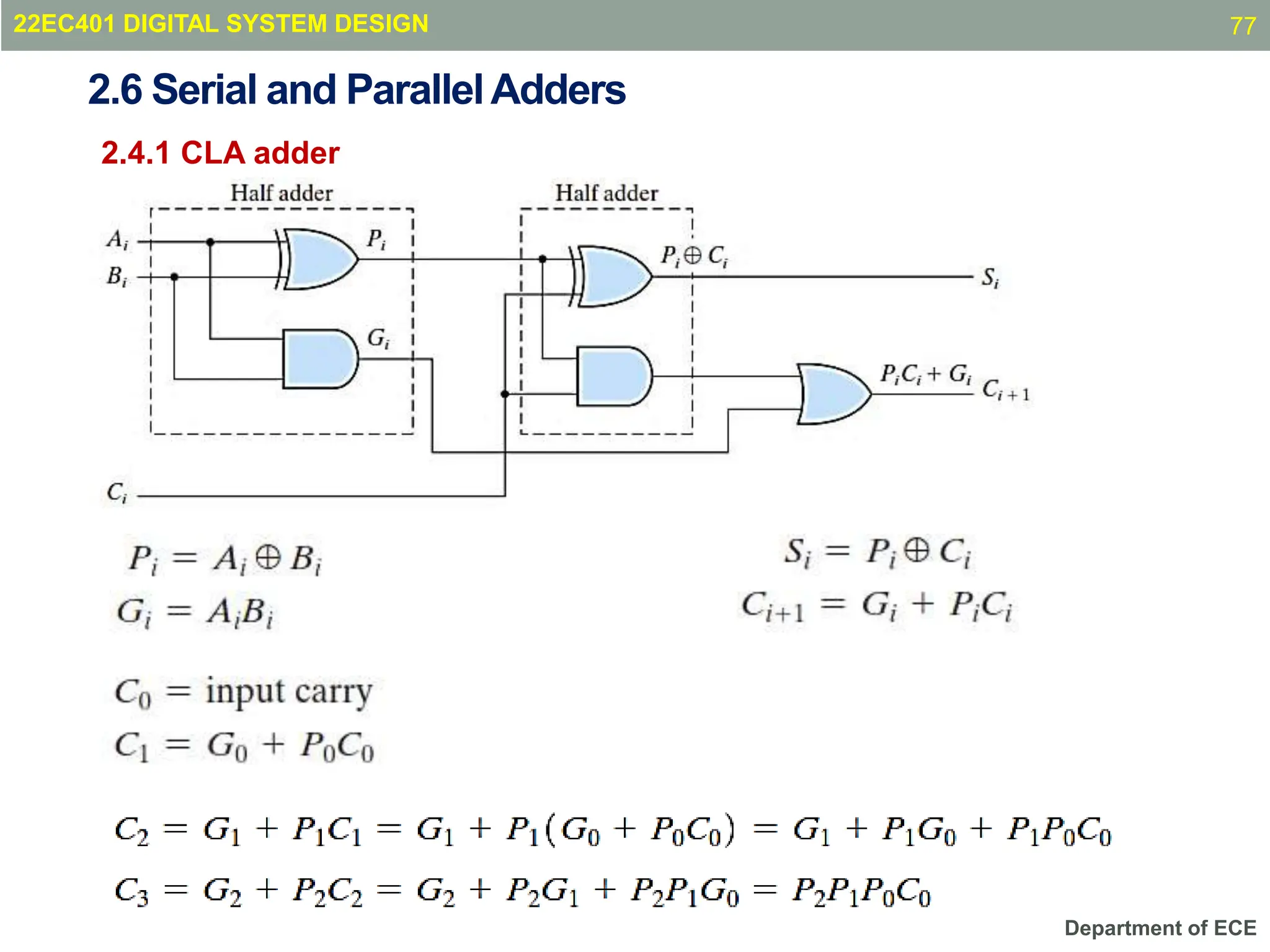
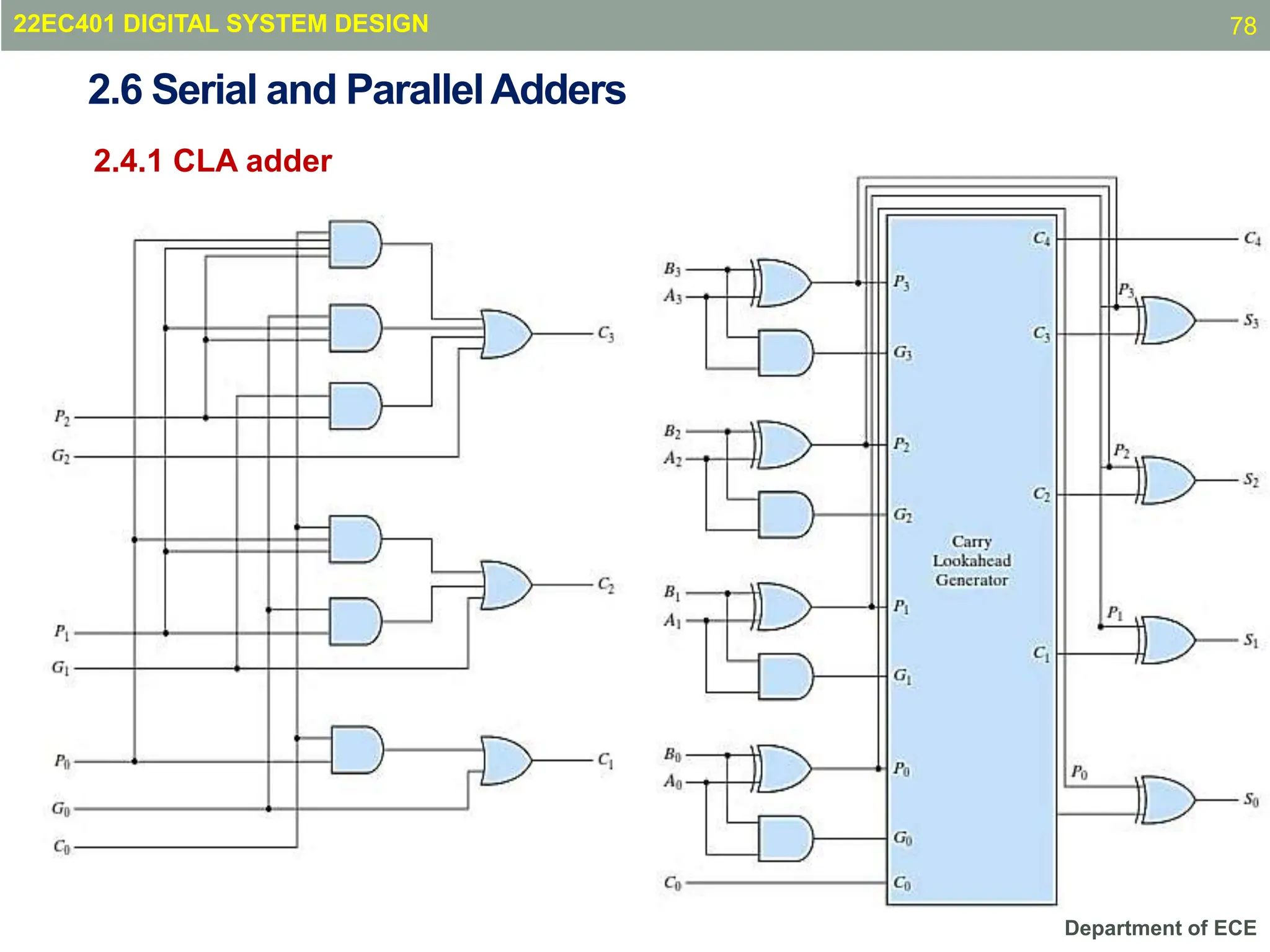
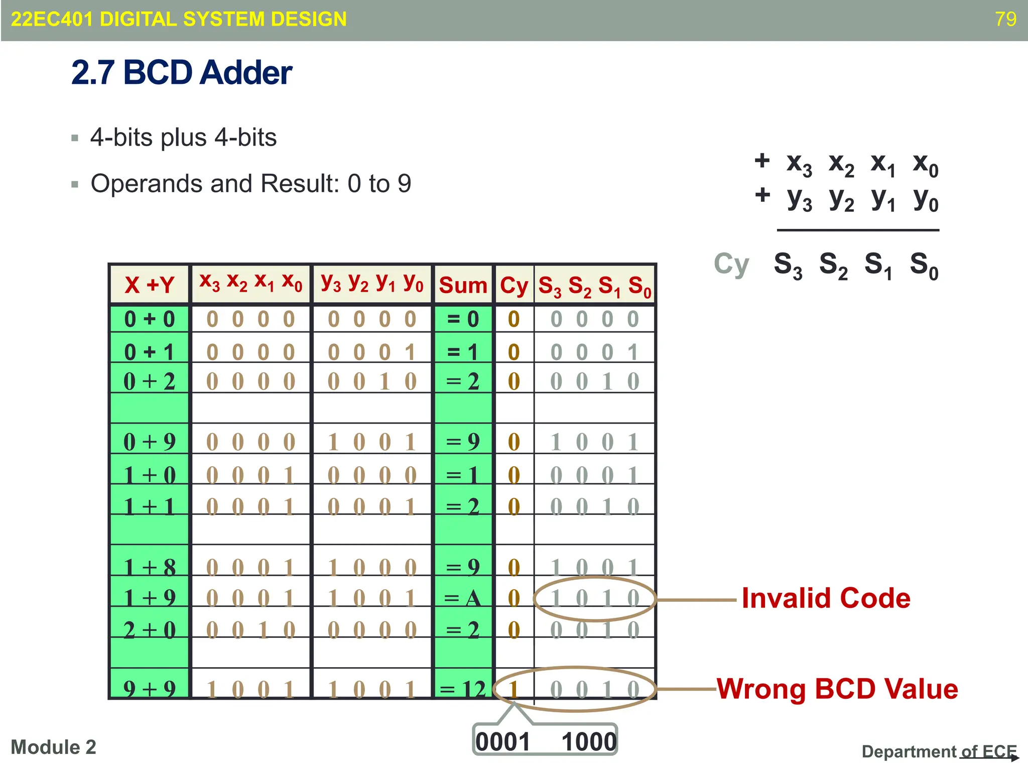
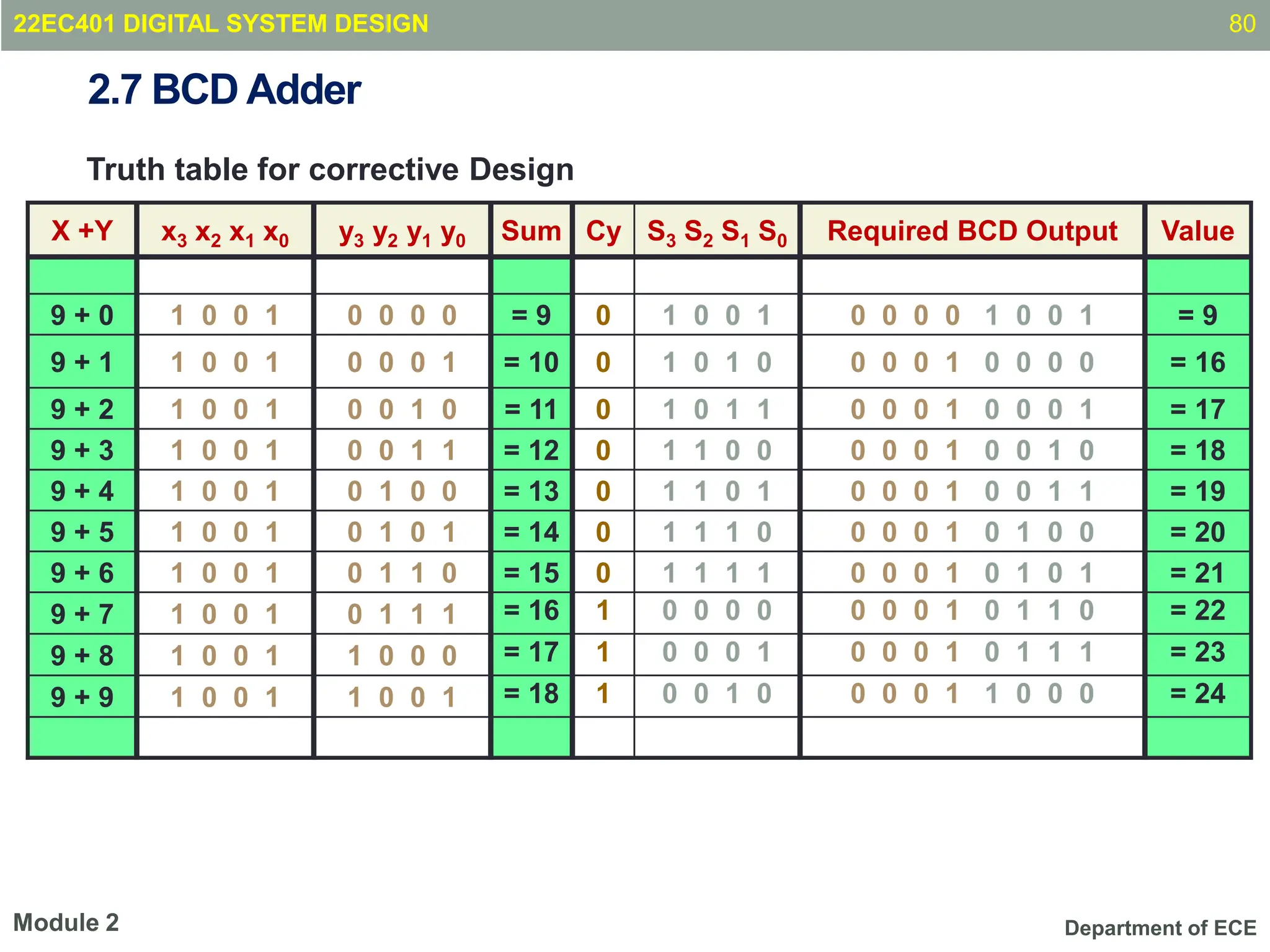
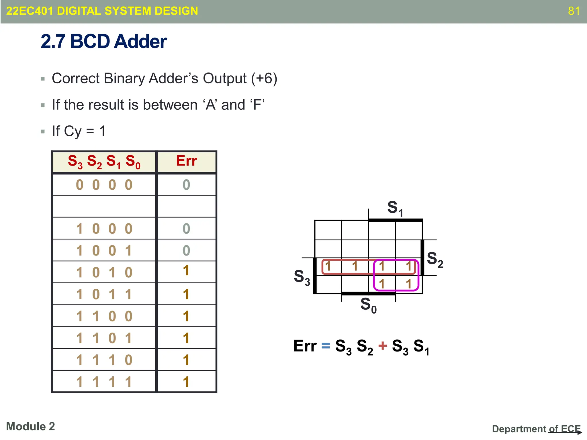
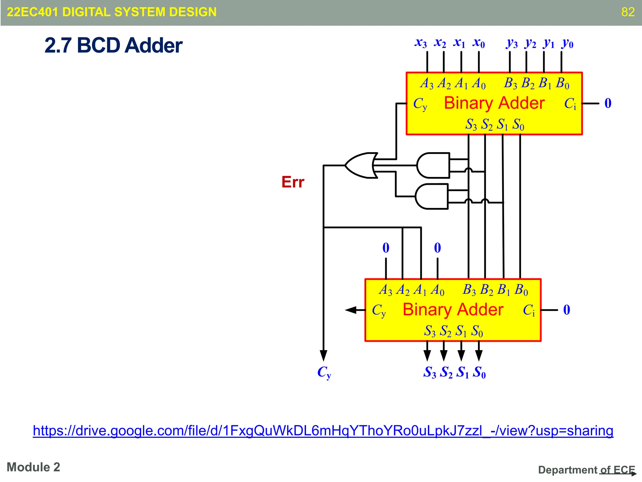
Combinational Circuits Design in Digital System Design.pptx
1. Department of ECE
22EC401 DIGITAL SYSTEM DESIGN
Class: II ECE
Academic Year: 2023-2024 (Even Sem)
MODULE I - LOGIC SIMPLIFICATION AND LOGIC FAMILIES
Course handling faculty: Mr.M.Navin Kumar, Dr.R.R.Thirrunavukkarasu, Dr.S.Prema
1
22EC401 DIGITAL SYSTEM DESIGN
2. Department of ECE
Syllabus:
Module 1: LOGIC SIMPLIFICATION AND LOGIC FAMILIES 15 Hrs
Logic Simplification: Review of Boolean Algebra and DeMorgan’s Theorem, SOP & POS
forms, Canonical forms, Karnaugh maps upto 4 variables, Quine McCluskey method,
Binary codes, Code Conversion. Logic families: Logic levels, propagation delay, power
dissipation, fan-out and fan-in, noise margin, logic families and their characteristics-RTL,
TTL, ECL, CMOS.
22EC401 DIGITAL SYSTEM DESIGN 2
Module II
Module 2: MSI COMBINATIONAL LOGIC CIRCUITS AND SEQUENTIAL LOGIC
DESIGN 15 Hrs
MSI devices like Comparators, Multiplexers, Encoder, Decoder, Half and Full Adders,
Subtractors, Serial and Parallel Adders, BCD Adder. Flip flops — SR, JK, T, D,
Master/Slave FF — operation and excitation tables, Triggering of FF, Analysis and design of
clocked sequential circuits — Design — Moore/Mealy models, state minimization, state
assignment, circuit implementation — Design of Counters- Ripple Counters, Ring Counters,
Shift registers, Universal Shift Register.
3. Department of ECE
Module contents
MSI COMBINATIONAL LOGIC CIRCUITS AND SEQUENTIAL
LOGIC DESIGN: MSI devices like Comparators, Multiplexers,
Encoder, Decoder, Half and Full Adders, Subtractors, Serial and
Parallel Adders, BCD Adder. Flip flops — SR, JK, T, D,
Master/Slave FF — operation and excitation tables, Triggering of
FF, Analysis and design of clocked sequential circuits — Design
— Moore/Mealy models, state minimization, state assignment,
circuit implementation — Design of Counters- Ripple Counters,
Ring Counters, Shift registers, Universal Shift Register.
22EC401 DIGITAL SYSTEM DESIGN 3
Module II
4. Department of ECE
2.1 Introduction
Traditional methods of combinational circuit design involve
simplification and realisation using gates.
Using these methods, complex functions have been integrated
(MSI) and are easily available in IC form.
Few examples are multiplexers, demultiplexers, adders, parity
generators/checkers, priority encoders, decoders,
comparators, etc.
4
Module 2
22EC401 DIGITAL SYSTEM DESIGN
5. Department of ECE
2.1 Introduction
Design is greatly simplified because the laborious and time
consuming simplification methods are generally not required.
Also improves the reliability of the system by reducing the
number of external wired connections.
To be familiar with the functions performed, the options
available, and the limitations of these devices in order to make
an effective and optimum use of such devices.
Usage of these devices significantly reduce IC package count
thereby reducing the system cost.
5
Module 2
22EC401 DIGITAL SYSTEM DESIGN
6. Department of ECE
2.2 Magnitude Comparator
2.2.1 Introduction
A magnitude digital Comparator is a combinational circuit that
compares two digital or binary numbers in order to find out
whether one binary number is equal, less than or greater than the
other binary number.
We logically design a circuit for which we will have two inputs one for
A and other for B and have three output terminals, one for A > B
condition, one for A = B condition and one for A < B condition.
6
Module 2
22EC401 DIGITAL SYSTEM DESIGN
https://drive.google.com/file/d/1NsqPt1svqlKAK3qT5ynx6i-2AWDsCm6a/view?usp=sharing
7. Department of ECE
2.2 Magnitude Comparator
2.2.2 1-Bit Magnitude Comparator
A comparator used to compare two bits is called a single bit comparator.
It consists of two inputs each for two single bit numbers and three outputs to
generate less than, equal to and greater than between two binary numbers.
The truth table for a 1-bit comparator is given below:
From the above truth table logical expressions for each output can be
expressed as follows:
A>B: AB'
A<B: A'B
A=B: A'B' + AB
7
Module 2
22EC401 DIGITAL SYSTEM DESIGN
8. Department of ECE
2.2 Magnitude Comparator
A comparator used to compare
two binary numbers each of two
bits is called a 2-bit Magnitude
comparator. It consists of four
inputs and three outputs to
generate less than, equal to and
greater than between two binary
numbers.
The truth table for a 2-bit
comparator is given below:
8
Module 2
2.2.3 2-Bit Magnitude Comparator
22EC401 DIGITAL SYSTEM DESIGN
9. Department of ECE
2.2 Magnitude Comparator
2.2.3 2-Bit Magnitude Comparator
From the above truth table K-map for each output can be drawn as follows:
9
Module 2
22EC401 DIGITAL SYSTEM DESIGN
11. Department of ECE
2.2 Magnitude Comparator
2.2.3 2-Bit Magnitude Comparator
11
Module 2
22EC401 DIGITAL SYSTEM DESIGN
12. Department of ECE
2.2 Magnitude Comparator
2.2.4 4-Bit Magnitude Comparator
A comparator used to compare two binary numbers each of four bits is called a
4-bit magnitude comparator.
It consists of eight inputs each for two four bit numbers and three outputs to
generate less than, equal to and greater than between two binary numbers.
In a 4-bit comparator the condition of A>B can be possible in the
following four cases:
If A3 = 1 and B3 = 0
If A3 = B3 and A2 = 1 and B2 = 0
If A3 = B3, A2 = B2 and A1 = 1 and B1 = 0
If A3 = B3, A2 = B2, A1 = B1 and A0 = 1 and B0 = 0
12
Module 2
22EC401 DIGITAL SYSTEM DESIGN
13. Department of ECE
2.2 Magnitude Comparator
2.2.4 4-Bit Magnitude Comparator
Similarly the condition for A<B can be possible in the following four cases:
If A3 = 0 and B3 = 1
If A3 = B3 and A2 = 0 and B2 = 1
If A3 = B3, A2 = B2 and A1 = 0 and B1 = 1
If A3 = B3, A2 = B2, A1 = B1 and A0 = 0 and B0 = 1
The condition of A=B is possible only when all the individual bits of one number
exactly coincide with corresponding bits of another number.
13
Module 2
22EC401 DIGITAL SYSTEM DESIGN
14. Department of ECE
2.2 Magnitude Comparator
2.2.4 4-Bit Magnitude Comparator
From the above statements logical expressions for each output can be
expressed as follows:
14
Module 2
Magnitude Comparator
A3A2A1A0 B3B2 B1 B0
A<B A=B A>B
3
3
3
3
3 B
A
B
A
x
2
2
2
2
2 B
A
B
A
x
1
1
1
1
1 B
A
B
A
x
0
0
0
0
0 B
A
B
A
x
0
1
2
3
)
( x
x
x
x
B
A
0
0
1
2
3
1
1
2
3
2
2
3
3
3
)
( B
A
x
x
x
B
A
x
x
B
A
x
B
A
B
A
0
0
1
2
3
1
1
2
3
2
2
3
3
3
)
( B
A
x
x
x
B
A
x
x
B
A
x
B
A
B
A
22EC401 DIGITAL SYSTEM DESIGN
15. Department of ECE
2.2 Magnitude Comparator
2.2.4 4-Bit Magnitude Comparator
15
Module 2
22EC401 DIGITAL SYSTEM DESIGN
16. Department of ECE
2.2 Magnitude Comparator
2.2.5 Cascading Comparator
A comparator performing the comparison operation to more than four bits by
cascading two or more 4-bit comparators is called cascading comparator. When
two comparators are to be cascaded, the outputs of the lower-order comparator
are connected to corresponding inputs of the higher-order comparator.
16
Module 2
22EC401 DIGITAL SYSTEM DESIGN
17. Department of ECE
2.2 Magnitude Comparator
2.2.6 Applications
1. Comparators are used in central processing units (CPUs) and
microcontrollers (MCUs).
2. These are used in control applications in which the binary numbers
representing physical variables such as temperature, position, etc.
are compared with a reference value.
3. Comparators are also used as process controllers and for Servo
motor control.
4. Used in password verification and biometric applications.
17
Module 2
22EC401 DIGITAL SYSTEM DESIGN
18. Department of ECE
2.3 Multiplexers
2.3.1 Introduction
The multiplexer (or data selector) is a logic circuit that allows one of the
data inputs at the output.
Figure shows a 4:1 Multiplexer with 4 input lines, 2 selection lines and 1
output line
18
Module 2
22EC401 DIGITAL SYSTEM DESIGN
https://drive.google.com/file/d/1bssbmNAP0OFe6clx4w_NFPp6ptYBvTN8/view?usp=sharing
19. Department of ECE
2.3 Multiplexers
2.3.1 4:1 Multiplexer
19
Module 2
22EC401 DIGITAL SYSTEM DESIGN
https://drive.google.com/file/d/1bssbmNAP0OFe6clx4w_NFPp6ptYBvTN8/view?usp=sharing
20. Department of ECE
2.3 Multiplexers
2.3.2 Multiplexers and their use in Combinational Logic Design
One of the most widely used standard logic circuits in digital design.
Because of its widespread use, it has been fabricated as MSI IC and is
commercially available in various sizes, such as 2:1, 4:1, 8:1, and 16:1
multiplexers.
https://drive.google.com/file/d/1zuDJmE3m9edehjoFDxTMntuGLeWN3kDv/view?usp=
sharing
20
Module 2
22EC401 DIGITAL SYSTEM DESIGN
21. Department of ECE
2.3 Multiplexers
2.3.2 Multiplexers and their use in Combinational Logic Design
21
Module 2
22EC401 DIGITAL SYSTEM DESIGN
22. Department of ECE
2.3 Multiplexers
2.3.3 A 4:1 Multiplexer with Strobe Input Using NAND Gates
22
Module 2
22EC401 DIGITAL SYSTEM DESIGN
23. Department of ECE
2.3 Multiplexers
32:1 Multiplexer Using
Two 16:1 Multiplexers
and One OR Gate
22EC401 DIGITAL SYSTEM DESIGN
https://drive.google.com/file/d/13nMAGW1V2AS5xN1wGePBg80bX-A_fTeP/view?usp=sharing
23
24. Department of ECE
2.3 Multiplexers
32.1
Multiplexer
Using Two 16:1
Multiplexers
and One 2:1
Multiplexer
22EC401 DIGITAL SYSTEM DESIGN 24
25. Department of ECE
2.3 Multiplexers
2.3.4 Combinational Logic Design Using Multiplexers
For using the multiplexer as a logic element, either the truth table or
one of the canonical forms of logic expression must be available. The
design procedure is given below:
1. Identify the decimal number corresponding to each minterm in the
expression. The input lines corresponding to these numbers are to
be connected to logic 1 level.
2. All other input lines are to be connected to logic 0 level.
3. The inputs are to be applied to select inputs.
25
Module 2
22EC401 DIGITAL SYSTEM DESIGN
26. Department of ECE
2.3 Multiplexers
2.3.4 Example: Implement the expression using a multiplexer
f (A, B, C, D) = Σm(0, 2, 3, 6, 8, 9, 12, 14)
Solution
Since there are four variables, therefore, a multiplexer with four select inputs is
required. The circuit of 16:1 multiplexer connected to implement the above
expression is shown in Fig.
This implementation requires only one IC package.
In case the output of the multiplexer is active-low, the logic 0 and logic 1 inputs
of Fig. are to be interchanged.
26
Module 2
22EC401 DIGITAL SYSTEM DESIGN
27. Department of ECE
2.3 Multiplexers
2.3.4 Example: Implement the expression using a multiplexer
f (A, B, C, D) = Σm(0, 2, 3, 6, 8, 9, 12, 14)
27
Module 2
22EC401 DIGITAL SYSTEM DESIGN
28. Department of ECE
2.3 Multiplexers
2.3.4 Realise the logic function of the truth table given in Table
28
Module 2
22EC401 DIGITAL SYSTEM DESIGN
29. Department of ECE
2.3 Multiplexers
2.3.4 Realise the logic function of the truth table given in Table
Solution
i. First Method: This can be realised using the method used in Example. Here,
the input lines 2, 4, 6, 7, 9, 10, 11, 12, and 15 are to be connected to logic 1
and the input lines 0, 1, 3, 5, 8, 13, and 14 are to be connected to logic 0.
29
Module 2
22EC401 DIGITAL SYSTEM DESIGN
30. Department of ECE
2.3 Multiplexers
2.3.4 Realise the logic function of the truth table given in Table
Solution
Second Method:
A four variable truth table or logic expression can be realised by using an 8:1
multiplexer instead of a 16:1 multiplexer. For this, partition the truth table as
shown by dotted lines. Here the inputs A, B, and C are to be connected to S2S
and S select inputs respectively. Now, we observe the relationship between
input D and output Y for each group of two rows.
There are four possible values of Y and these are 0, 1, D, and D’. These are
given in Table. From this table, we note the output Y for each of the
combinations of A, B, and C, and then make the connections accordingly. The
implementation of this function using an 8:1 multiplexer is shown in Fig.
30
Module 2
22EC401 DIGITAL SYSTEM DESIGN
31. Department of ECE
2.3 Multiplexers
2.3.4 Realise the logic function of the truth table given in Table
31
Module 2
22EC401 DIGITAL SYSTEM DESIGN
32. Department of ECE
2.3 Multiplexers
2.3.4 Realise the logic function of the truth table given in Table
32
Module 2
22EC401 DIGITAL SYSTEM DESIGN
33. Department of ECE
2.3 Multiplexers
2.3.4 Realise the logic function of the truth table given in Table
33
Module 2
22EC401 DIGITAL SYSTEM DESIGN
34. Department of ECE
2.3 Multiplexers
2.3.5 Demultiplexer
The Demultiplexer performs the reverse operation of a multiplexer. It
accepts a single input and distributes it over several outputs. Figure
gives the block diagram of a Demultiplexer. The select input code
determines to which output the data input will be transmitted.
34
Module 2
22EC401 DIGITAL SYSTEM DESIGN
https://drive.google.com/file/d/1T5MKJsXtuJRwaNUMRP-ueoCWDO3up5ww/view?usp=sharing
35. Department of ECE
2.3 Multiplexers
2.3.5 Demultiplexer
• The number of output lines is n and the number of select lines is m,
where n = 2m.
• The data input D will appear on the output line selected by the select
input.
• For example, if the decimal equivalent of the select input is 4, then the
data will appear on D4 output line.
• This circuit can also be used as binary-to-decimal decoder
35
Module 2
22EC401 DIGITAL SYSTEM DESIGN
36. Department of ECE
2.3 Multiplexers
2.3.5 Demultiplexer/Decoder
This circuit can also be used as binary-to-decimal decoder with binary
inputs applied at the select input lines and the output will be obtained
on the corresponding line. The data input line is to be connected to
logic 1 level.
36
Module 2
22EC401 DIGITAL SYSTEM DESIGN
37. Department of ECE
2.3 Multiplexers
2.3.6 Example:
Implement the following multi-output combinational logic circuit using a 4-
to-16-line decoder.
F1 = Σm (1, 2, 4, 7, 8, 11, 12, 13)
F2 = Σm (2, 3, 9, 11)
F3 = Σm (10, 12, 13, 14)
F4 = Σm (2, 4, 8)
37
Module 2
22EC401 DIGITAL SYSTEM DESIGN
38. Department of ECE
2.3 Multiplexers
2.3.6 Example:
Solution
• The four-bit input ABCD is applied at the Select input terminals S3, S2, S1, and
S0. The output F1 is required to be 1 for minterms 1, 2, 4, 7, 8, 11, 12, and 13.
• Therefore, a NAND gate is connected as shown.
• Similarly NAND gates are used for the outputs F2, F3, and F4.
• Here, the decoder’s outputs are active-low, therefore a NAND gate is required
for every output of the combinational circuit.
38
Module 2
22EC401 DIGITAL SYSTEM DESIGN
39. Department of ECE
2.3 Multiplexers
2.3.6 Example:
Realization
39
Module 2
22EC401 DIGITAL SYSTEM DESIGN
40. Department of ECE
2.4 Decoder, Encoder & Priority Encoder
Extract “Information” from the code
Binary Decoder
Example: 2-bit Binary Number
Binary
Decoder
x1
x0
Only one
lamp will
turn on
0
0
1
0
0
0
2.4.1 Decoder
22EC401 DIGITAL SYSTEM DESIGN
https://drive.google.com/file/d/1Hjeh3GabRyMgsYVAKwhO0DI3V4SKEi0S/view?usp=sharing
40
41. Department of ECE
2-to-4 Line Decoder
I1 I0 Y3 Y2 Y1 Y0
0 0 0 0 0 1
0 1 0 0 1 0
1 0 0 1 0 0
1 1 1 0 0 0
Binary
Decoder
I1
I0
y3
y2
y1
y0
I1
I0
Y3
Y2
Y1
Y0
0
1
3 I
I
Y 0
1
2 I
I
Y
0
1
1 I
I
Y 0
1
0 I
I
Y
2.4 Decoder, Encoder & Priority Encoder
2.4.1 Decoder
22EC401 DIGITAL SYSTEM DESIGN 41
42. Department of ECE
3-to-8 Line Decoder
Binary
Decoder
I2
I1
I0
Y7
Y6
Y5
Y4
Y3
Y2
Y1
Y0
I2
I0
Y7
Y6
Y5
Y4
Y3
Y2
Y1
Y0
I1
0
1
2 I
I
I
0
1
2 I
I
I
0
1
2 I
I
I
0
1
2 I
I
I
0
1
2 I
I
I
0
1
2 I
I
I
0
1
2 I
I
I
0
1
2 I
I
I
2.4 Decoder, Encoder & Priority Encoder
2.4.1 Decoder
22EC401 DIGITAL SYSTEM DESIGN 42
43. Department of ECE
“Enable” Control
Binary
Decoder
I1
I0
E
Y3
Y2
Y1
Y0
E I1 I0 Y3 Y2 Y1 Y0
0 x x 0 0 0 0
1 0 0 0 0 0 1
1 0 1 0 0 1 0
1 1 0 0 1 0 0
1 1 1 1 0 0 0
E
I0
Y3
Y2
Y1
Y0
I1
2.4 Decoder, Encoder & Priority Encoder
2.4.1 Decoder
22EC401 DIGITAL SYSTEM DESIGN 43
46. Department of ECE
Each output is a minterm
All minterms are produced
Sum the required minterms
Example: Full Adder
S(x, y, z) = ∑(1, 2, 4, 7)
C(x, y, z) = ∑(3, 5, 6, 7)
I2
I1
I0
Y7
Y6
Y5
Y4
Y3
Y2
Y1
Y0
Binary Decoder
x
y
z
S C
2.4 Decoder, Encoder & Priority Encoder
2.4.1 Decoder
22EC401 DIGITAL SYSTEM DESIGN
https://drive.google.com/file/d/1m6lTCZD0S5fkIEQpMWPV8UVaAcA0Nsba/view?usp=sharing
46
47. Department of ECE
2.4.1 Implementation Using Decoders
I2
I1
I0
Y7
Y6
Y5
Y4
Y3
Y2
Y1
Y0
Binary
Decoder
x
y
z
S C
I2
I1
I0
Y7
Y6
Y5
Y4
Y3
Y2
Y1
Y0
Binary
Decoder
x
y
z
S C
22EC401 DIGITAL SYSTEM DESIGN
2.4 Decoder, Encoder & Priority Encoder
47
48. Department of ECE
Implementation Using Decoders
22EC401 DIGITAL SYSTEM DESIGN
Implement the following multi-output combinational logic circuit using a 4-to-16-line
decoder.
F1 = Σm (1, 2, 4, 7, 8, 11, 12, 13)
F2 = Σm (2, 3, 9, 11)
F3 = Σm (10, 12, 13, 14)
F4 = Σm (2, 4, 8)
2.4 Decoder, Encoder & Priority Encoder
48
49. Department of ECE
Implementation Using Decoders
22EC401 DIGITAL SYSTEM DESIGN 49
Module 2
The four-bit input ABCD is applied at the Select input terminals S
3
, S
2
, S
1
, and S
0
.
The output F
1
is required to be 1 for minterms 1, 2, 4, 7, 8, 11, 12, and 13. Therefore,
a NAND gate is connected as shown. Similarly NAND gates are used for the outputs
F
2
, F
3
and F
4
. Here, the decoder’s outputs are active-low, therefore a NAND gate is
required for every output of the combinational circuit.
2.4 Decoder, Encoder & Priority Encoder
50. Department of ECE
2.4.2 Encoders
Put “Information” into code
Binary Encoder
Example: 4-to-2 Binary Encoder
x3 x2 x1 y1 y0
0 0 0 0 0
0 0 1 0 1
0 1 0 1 0
1 0 0 1 1
Binary
Encoder
y1
y0
x1
x2
x3
Only one
switch
should be
activated at a
time
22EC401 DIGITAL SYSTEM DESIGN
2.4 Decoder, Encoder & Priority Encoder
50
51. Department of ECE
2.4.2 Encoders
Octal-to-Binary Encoder (8-to-3)
I7 I6 I5 I4 I3 I2 I1 I0 Y2 Y1 Y0
0 0 0 0 0 0 0 1 0 0 0
0 0 0 0 0 0 1 0 0 0 1
0 0 0 0 0 1 0 0 0 1 0
0 0 0 0 1 0 0 0 0 1 1
0 0 0 1 0 0 0 0 1 0 0
0 0 1 0 0 0 0 0 1 0 1
0 1 0 0 0 0 0 0 1 1 0
1 0 0 0 0 0 0 0 1 1 1
Binary
Encoder
Y2
Y1
Y0
I7
I6
I5
I4
I3
I2
I1
I0
1
3
5
7
0
2
3
6
7
1
4
5
6
7
2
I
I
I
I
Y
I
I
I
I
Y
I
I
I
I
Y
I7
I6
I5
I4
I3
I2
I1
I0
Y2
Y1
Y0
22EC401 DIGITAL SYSTEM DESIGN
2.4 Decoder, Encoder & Priority Encoder
51
52. Department of ECE
2.4.3 Priority Encoders
4-Input Priority Encoder
I3 I2 I1 I0 Y1 Y0 V
0 0 0 0 0 0 0
0 0 0 1 0 0 1
0 0 1 x 0 1 1
0 1 x x 1 0 1
1 x x x 1 1 1
Priority
Encoder
V
Y1
Y0
I3
I2
I1
I0
I0
I1
I2
I3
Y1
Y0
V
0
1
2
3
1
2
3
0
2
3
1
I
I
I
I
V
I
I
I
Y
I
I
Y
Y1 I1
1 1 1 1
I2
I3
1 1 1 1
1 1 1 1
I0
22EC401 DIGITAL SYSTEM DESIGN
2.4 Decoder, Encoder & Priority Encoder
https://drive.google.com/file/d/1T59H03KvUe87PgP3Ug1MOokTPLHu1z1j/view?usp=sharing
52
54. Department of ECE
2.5 Half and FullAdders & Subtractors
2.5.1 Introduction
An adder is a digital logic circuit in electronics that implements
addition of numbers.
In many computers and other types of processors, adders are used to
calculate addresses, similar operations and table indices in the ALU
and also in other parts of the processors.
These can be built for many numerical representations like excess-3
or binary coded decimal.
Adders are classified into two types: Half adder and Full adder.
54
Module 2
22EC401 DIGITAL SYSTEM DESIGN
https://drive.google.com/file/d/1sJ6YVqvb0xQCd0VCsva2Q_pw7CuGqY5w/view?usp=sharing
55. Department of ECE
2.5 Half and FullAdders & Subtractors
2.5.1 Half Adder
The half adder circuit has two inputs: A and B, which add two input
digits and generate a Carry (C) and Sum (S)
The half adder adds two binary digits called as augend and addend
and produces two outputs as sum and carry; XOR is applied to both
inputs to produce sum and AND gate is applied to both inputs to
produce carry.
55
Module 2
22EC401 DIGITAL SYSTEM DESIGN
https://drive.google.com/file/d/1H4x1jlwPRtm3yMcT_h47HbYDVuvIIlS_/view?usp=sharing
56. Department of ECE
2.5 Half and FullAdders & Subtractors
2.5.1 Design of Half adder
By using half adder, you can design simple addition with the help of
logic gates.
Let’s see an addition of single bits.
0+0 = 0
0+1 = 1
1+0 = 1
1+1 = 10
56
Module 2
22EC401 DIGITAL SYSTEM DESIGN
57. Department of ECE
2.5 Half and FullAdders & Subtractors
2.5.1 Design of Half adder
These are the least possible single-bit combinations. But the result for
1+1 is 10, the sum result must be re-written as a 2-bit output. Thus, the
equations can be written as
0+0 = 00
0+1 = 01
1+0 = 01
1+1 = 10
The output ‘1’of ‘10’ is carry-out. ‘SUM’ is the normal output and
‘CARRY’ is the carry-out.
57
Module 2
22EC401 DIGITAL SYSTEM DESIGN
58. Department of ECE
2.5 Half and FullAdders & Subtractors
2.5.1 Design of Half adder
Truth table
Now it has been cleared that 1-bit adder can be easily implemented
with the help of the XOR Gate for the output ‘SUM’ and an AND Gate
for the ‘Carry’.
The half-adder is useful when you want to add one binary digit
quantities.
58
Module 2
22EC401 DIGITAL SYSTEM DESIGN
59. Department of ECE
2.5 Half and FullAdders & Subtractors
2.5.1 Design of Half adder
Design
• The simplest expression uses the exclusive OR function: Sum=A B.
• An equivalent expression in terms of the basic AND, OR, and NOT is:
SUM=A’.B+A.B’
59
Module 2
22EC401 DIGITAL SYSTEM DESIGN
60. Department of ECE
2.5 Half and FullAdders & Subtractors
2.5.1 Design of Half adder
Design
60
Module 2
22EC401 DIGITAL SYSTEM DESIGN
61. Department of ECE
2.5 Half and FullAdders & Subtractors
2.5.2 Full Adder
This type of adder is a little more difficult to implement than a half-
adder.
The main difference between a half-adder and a full-adder is that the
full-adder has three inputs and two outputs.
The first two inputs are A and B and the third input is an input carry
designated as Cin.
When a full adder logic is designed we will be able to string eight of
them together to create a byte-wide adder and cascade the carry bit
from one adder to the next.
61
Module 2
22EC401 DIGITAL SYSTEM DESIGN
https://drive.google.com/file/d/1vj-0WyD0LqhE89VFQjls19J17xXoLXoC/view?usp=sharing
62. Department of ECE
2.5 Half and FullAdders & Subtractors
2.5.2 Full Adder
The full adder circuit has three inputs: A, B and Cin, which add the
three input numbers and generate output carry (Cout) and sum (S).
The full adder adds 3 one bit numbers, where two can be referred to
as operands (A & B) and one can be referred to as bit carried in (Cin)
and produces 2-bit output, and these can be referred to as output
carry (Cout) and sum (S).
62
Module 2
22EC401 DIGITAL SYSTEM DESIGN
https://drive.google.com/file/d/1fkq0hXMG_YQfTryRxnGMpq-Cbop-NGuo/view?usp=sharing
63. Department of ECE
2.5 Half and FullAdders & Subtractors
2.5.3 Half Subtractor
Half Subtractor is used for the purpose of subtracting two single bit numbers.
Half subtractors have no scope of taking into account “Borrow-in” from the
previous circuit.
To overcome this drawback, full subtractor comes into play.
63
Module 2
22EC401 DIGITAL SYSTEM DESIGN
https://drive.google.com/file/d/11rQoxpCGHsWcqMcT5VMNEl7Bl3amavKk/view?usp=sharing
64. Department of ECE
2.5 Half and FullAdders & Subtractors
2.5.3 Half Subtractor Design
64
Module 2
22EC401 DIGITAL SYSTEM DESIGN
Inputs Outputs
A B D (Difference) b (Borrow)
0 0 0 0
0 1 1 1
1 0 1 0
1 1 0 0
65. Department of ECE
2.5 Half and FullAdders & Subtractors
2.5.4 Full Subtractor
Full Subtractor is a combinational logic circuit.
It is used for the purpose of subtracting two single bit numbers.
It also takes into consideration borrow of the lower significant stage.
Thus, full subtractor has the ability to perform the subtraction of three bits.
Full subtractor contains 3 inputs and 2 outputs (Difference and Borrow) as
shown-
65
Module 2
22EC401 DIGITAL SYSTEM DESIGN
https://drive.google.com/file/d/1Unow3pvAvygc_kk4c5rAE_Rks1PeridA/view?usp=sharing
66. Department of ECE
2.5 Half and FullAdders & Subtractors
2.5.4 Full Subtractor Design
66
Module 2
22EC401 DIGITAL SYSTEM DESIGN
Inputs
Outputs
A B Bin
Bout
(Borrow)
D
(Difference)
0 0 0 0 0
0 0 1 1 1
0 1 0 1 1
0 1 1 1 0
1 0 0 0 1
1 0 1 0 0
1 1 0 0 0
1 1 1 1 1
67. Department of ECE
2.6 Serial and ParallelAdders
2.6.1 Introduction
As, we already know, a full adder was used to add two 1-bit binary
numbers and the additional carry bit (Cin).
But, to add two n-bit binary numbers, we will require n-number of full
adders.
The carry-out of each full-adder is also connected to the carry-in of the
next full-adder in the higher-order.
A Binary Parallel adder is used to add two numbers in parallel form
and to produce the sum bits as parallel outputs.
In two numbers, one is addend and the other is augend and both are
added parallelly to get the sum.
67
Module 2
22EC401 DIGITAL SYSTEM DESIGN
68. Department of ECE
2.6.1 Introduction
As, we already know, a full adder was used to add two 1-bit binary
numbers and the additional carry bit (Cin).
But, to add two n-bit binary numbers, we will require n-number of full
adders.
The carry-out of each full-adder is also connected to the carry-in of the
next full-adder in the higher-order.
A Binary Parallel adder is used to add two numbers in parallel form
and to produce the sum bits as parallel outputs.
In two numbers, one is addend and the other is augend and both are
added parallelly to get the sum.
68
Module 2
2.6 Serial and ParallelAdders
22EC401 DIGITAL SYSTEM DESIGN
https://drive.google.com/file/d/1zr59hARmII5xIEjOtus_3xobI-SJmGHD/view?usp=sharing
69. Department of ECE
2.4.1 Binary Parallel Adder
Two n+1-bit binary number A and B of the form
A: An An-1 An-2 ... A3 A2 A1 A0 (Augend)
B: Bn Bn-1 Bn-2 ... B3 B2 B1 B0 (Addend)
4-bit Parallel adder
In the block diagram, A0 and B0 represent the LSB of the four-bit
words A and B
69
Module 2
2.6 Serial and ParallelAdders
22EC401 DIGITAL SYSTEM DESIGN
https://drive.google.com/file/d/1YFGYTYM6YQawloFhNx_eTQYne94SUrV8/view?usp=sharing
70. Department of ECE
c3 c2 c1 .
+ x3 x2 x1 x0
+ y3 y2 y1 y0
────────
Cy S3 S2 S1 S0
FA
x3 x2 x1 x0
FA
FA
FA
y3 y2 y1 y0
S3 S2 S1 S0
C4 C3 C2 C1
0
Binary Adder
x3x2x1x0 y3y2y1y0
S3S2S1S0
C0
Cy
Carry
Propagate
Addition
2.4.1 Binary Parallel Adder
Module 2
2.6 Serial and ParallelAdders
22EC401 DIGITAL SYSTEM DESIGN 70
72. Department of ECE
2.4.2 CLA adder
Motivation behind Carry Look-Ahead Adder :
In ripple carry adders, for each adder block, the two bits that are to be
added are available instantly.
However, each adder block waits for the carry to arrive from its
previous block.
So, it is not possible to generate the sum and carry of any block until
the input carry is known.
The ith block waits for the i-1th block to produce its carry. So there will
be a considerable time delay which is carry propagation delay.
72
Module 2
2.6 Serial and ParallelAdders
22EC401 DIGITAL SYSTEM DESIGN
https://drive.google.com/file/d/17z_g6l-MCTLMgvOj4reRUVsdptrVylPs/view?usp=sharing
https://drive.google.com/file/d/1N7H_GgZU3JN6bzUimKHi45FlqmvKJXHJ/view?usp=sharing
73. Department of ECE
2.4.2 CLA adder
Motivation behind Carry Look-Ahead Adder :
Consider the above 4-bit ripple carry adder. The sum S4 is produced by the
corresponding full adder as soon as the input signals are applied to it.
But the carry input C4 is not available on its final steady state value until carry
C3 is available at its steady state value.
Similarly C3 depends on C2 and C2 on C1.
Therefore, though the carry must propagate to all the stages in order that
output S3 and carry C4 settle their final steady-state value.
73
Module 2
2.6 Serial and ParallelAdders
22EC401 DIGITAL SYSTEM DESIGN
74. Department of ECE
2.4.2 CLA adder
Motivation behind Carry Look-Ahead Adder :
Consider the above 4-bit ripple carry adder. The sum S4 is produced by the
corresponding full adder as soon as the input signals are applied to it.
But the carry input C4 is not available on its final steady state value until carry
C3 is available at its steady state value.
Similarly C3 depends on C2 and C2 on C1.
Therefore, though the carry must propagate to all the stages in order that
output S3 and carry C4 settle their final steady-state value.
74
Module 2
2.6 Serial and ParallelAdders
22EC401 DIGITAL SYSTEM DESIGN
75. Department of ECE
2.4.2 CLA adder
Motivation behind Carry Look-Ahead Adder :
The propagation time is equal to the propagation delay of each adder block,
multiplied by the number of adder blocks in the circuit.
For example, if each full adder stage has a propagation delay of 20
nanoseconds, then S3 will reach its final correct value after 60 (20 × 3)
nanoseconds.
The situation gets worse, if we extend the number of stages for adding more
number of bits.
Carry Look-ahead Adder :
A carry look-ahead adder reduces the propagation delay by introducing more
complex hardware. In this design, the ripple carry design is suitably transformed
such that the carry logic over fixed groups of bits of the adder is reduced to two-
level logic.
75
Module 2
2.6 Serial and ParallelAdders
22EC401 DIGITAL SYSTEM DESIGN
76. Department of ECE
2.4.1 CLA adder
Carry Look-ahead Adder :
Consider the full adder circuit shown with corresponding truth table. We define
two variables as ‘Carry Generate’ (Gi) and ‘Carry Propagate’ (Pi) then,
76
Module 2
2.6 Serial and ParallelAdders
22EC401 DIGITAL SYSTEM DESIGN
77. Department of ECE
2.4.1 CLA adder
2.6 Serial and ParallelAdders
22EC401 DIGITAL SYSTEM DESIGN 77
78. Department of ECE
2.4.1 CLA adder
2.6 Serial and ParallelAdders
22EC401 DIGITAL SYSTEM DESIGN 78