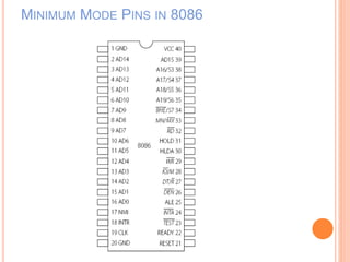
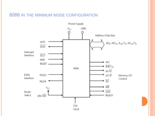
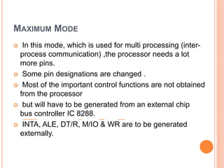
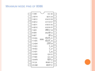
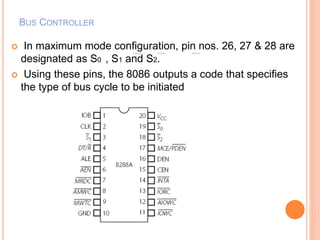
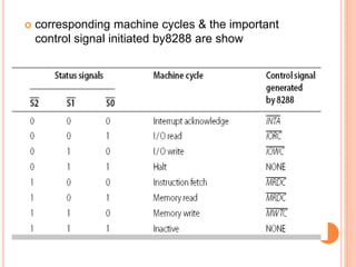
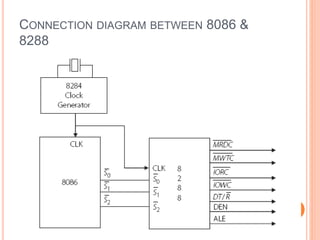
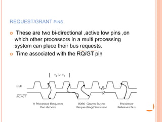
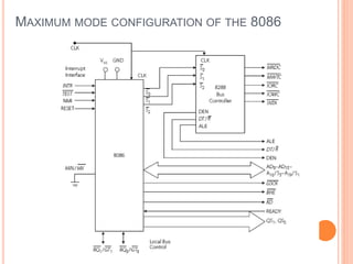
SlideShare a Scribd company logo
THE HARDWARE
STRUCTURE OF 8086
CHAPTER 6
 In this chapter we will discuss on:
1. Difference between 8086 & 8088
2. Pin functions of 8086 in minimum & maximum modes
3. use of address latches & data buffers in an 8086 based
system
4. concept of machine cycles and the associated bus timings
of 8086
5. reason for using the bus controller IC in a maximum mode
system
6. How an 8086 is used in the maximum mode?
7. To calculate instruction timing & thus create delay loops
 Earlier we have dealt exclusively with the programming
aspect of 8086, now we will see for hardware aspects of the
processor.
PIN CONFIGURATION
 Lets see the processor in terms of its hardware that
includes:
Pin configuration
Functions of the pins
memory bus cycles
connections to other chips
modes of operations
 The first PC was built with 8088 processor & most ways
similar to 8086
DIFFERENCE BETWEEN 8088 & 8086
i. 8088 has an external data bus of 8 bits, while 8086 has a
16-bit data bus
ii. Instruction queue of 8088 is 4 bytes, while 8086 has a
16-byte queue
iii. for 8088, pin no.28 (minimum mode) is an M / IO pin,
while for 8086, the pin is M/IO
iv. Pin no. 34 is SSO for 8088, while it is BHE / S7 for 8086
8088 & 8086 CPU PIN DIAGRAM
8086 Pin8088 Pin
 Pin diagrams of both processor are shown
 Both processors are packaged as 40-pin DIP (dual-in-line
package) .
 Some pins are dual functions corresponds to minimum &
maximum modes
 Minimum mode –when used in uni-processor configuration
 Maximum mode –when used in multi-processor
configuration
 Here we will discuss the hardware aspects of 8086
 It is the basic processor in the X86 family
MINIMUM MODE PINS IN 8086
 pins 24 to 31 have are seen to have dual functions
 functions in bracket indicate the pin designation to be in
the minimum mode for those pins
 for min mode operation, pin no.33 MN/MX should be at
logic high
 we know that 8086 has a 16-bit data bus & 20-bit address
bus
 Lets locate the address & data pins in the pin diagram
 We can see a set of 16 pins designated as AD, i.e AD0 –
AD15
 They are address/data pins
 Notation ‘AD’ means that these pins are used for address
as well as data
 They are multiplexed for data & address, such that at a
particular time they carry address & at other time s they
carry data
 Reason for multiplexing is to reduce the number of pins of
the chip
 8086 has only 40 pin counts
 As the data bus & address bus have to be separate &
because the ‘address’ has to be available at all times
 the address-data lines have to be de-multiplexed means
separated
 this can be done by the use of latches
 availing the timing features of bus cycles
DE-MULTIPLEXING THE ADDRESS/ DATA BUS
 The action of separating address and data is called
de-multiplexing
 lets see that, memory is to be read from or written to
 W.K.T there are some steps involved for reading & writing
memory
 first step in reading memory is ‘placing the address on the
address bus’
 This is the 1st part of the bus cycle
 Next, to appear data on the data bus, means the bus must be
made free to carry data
 for de-multiplexing, during the time that the address is in the
address/data bus, it is to be latched on to a ‘Latch IC’ whose
clock is ALE(Address latch enable) signal supplied to 8086
 Signal ALE goes high & functions as a clock for a latch that is
used to save the address value, as the address has to be
available throughout the bus cycle
 Once the address is latched on to the latches, it can be removed
from the AD lines, then these lines are free to carry data.
 This action is only for 16 address lines
 But 8086 has 20-bit address
 So, in pin diagram, pin numbers 35 to 38 also used for
address
 They are A16 to A19
 They are also multiplexed with status signals
 Diagram for address/data de-multiplexing
DE-MULTIPLEXED ADDRESS BUS
 We know what is de-multiplexing?
 To make sure that address is available on the memory or I/O
address throught the complete read/write bus cycle
 with 20 lines of address information & line BHE have to be
latched & output of latch will constitute the address bus.
 So, 21 lines are to be latched with the help of external ICs
 One very popular latch IC is the 3 state octal transparent latch
74LS373
 As one IC have only to 8 lines, 3 such latches are needed for de-
multiplexing
 Pin diagram shows how IC appears
 The data sheet of this IC specifies that, all the 8 latches of this
74LS373 is D-type latch
 Means that while enable (G) is HIGH, the Q outputs will follow
the D-inputs.
 Here ALE is connected to the G pin of the IC
 The OC (output control) is grounded for normal
operation.
DE-MULTIPLEXING DATA BUS
CONTROL SIGNALS FOR READ & WRITE
 Before going to discussion on bus timings
 we should know about the associated control signals RD ,
WR, M/IO may also be buffered
 as the output signals are sent out by 8086
 these lines are unidirectional
 hence the buffer IC74LS244 is sufficient to use.
 This is a unidirectional tri-state octal buffer
MEMORY AND I / O
 Signals RD, WR, M/IO have to be used suitably to get
the memory read/write
 as MEMRD and MEMWR and the I/O read/write signals
IORD and IOWR
 the circuit diagram shows the I/O and Memory having
seprate lines for access.
CLOCK GENERATION
 One cycle of the clock is called a T state, and all timings and
delays are multiples of this T state duration.
 8086 to have a clock signal
 There is no circuitry inside the processor for
this, and so an external clock generator IC is used.
 Intel has provided the clock generator IC 8284A which is
compatible with 8086 / 8088.
 This generates based on the crystal connected between
two of its terminal
 crystal frequency should be 3 times the desired frequency
for the microprocessor
 so 8086 operates at frequencies of 5 to 15 MHz
 We see the basic functions associated with minimum
modes systems
PIN CONFIGURATION OF THE CLOCK GENERATOR
8284A
CLOCK GENERATOR IC
 The clock generator IC performs a few more
functions than just supplying the clock frequency to
the processor.
 The crystal is connected between the X1 and X2
pins.
 The READY output pin of 8284A is connected to
the READY input pin of 8086.
 This pin is used to overcome the timing
inconsistencies that are possible when a slow
peripheral / memory device is connected to the
processor.
 Extra wait states are inserted when READY signal
is low.
CONNECTIONS OF THE CLOCK GENERATOR IC
TO 8086
RESET
 An active low reset signal from the control bus is
sent to the 8284 which synchronizes it with the
trailing edge of the clock.
 Most systems include a line that goes to all system
components and possibly controlled by an operator
push button (or just after power on), which causes a
low signal on the RESET pin of the clock
generator.
RESET TIMINGS AND RESET VECTOR
 The RESET line of 8086 must remain high for at
least 4 clock periods.
 The 8086 will terminate operations on the high-
going edge of RESET and will remain dormant as
long as RESET is HIGH.
 A high on the RESET pin of the processor causes
all system components to be reset, and inside it,
the instruction queue, PSW, DS, SS, ES and IP are
cleared.
 CS gets a value of FFFFH and with IP = 0000, the
first instruction will be executed from the location
FFFF0H.
POWER ON RESET
 When power is switched on, the 8086 should be RESET.
 This is called power on reset
CLOCK
 All activities on the system bus are synchronized by the
system clock
 that provides the basic timing
 Activities of the Bus are:
1. Reading from memory I/O
2. Writing to memory I/O
 Any read or write cycle is called a bus cycle.
 For 8086, a bus cycle takes 4 T states, where one T state is
defined as the ‘period’ of the clock.
 If the clock frequency is 10 MHz, one T state = 0.1 usecs
or 100 nsecs.
 A bus cycle is also called a machine cycle.
 During a machine cycle, a specific operation – say, reading
or writing is accomplished.
TYPICAL MACHINE CYCLES
 Memory Read
 Memory Write
 I / O Read
 I / O Write
 Interrupt Acknowledge
READ MACHINE CYCLE
 Place on the address bus, the address of the location whose
content is to be read. This action is performed by the
processor.
 Assert the read control signal which is part of the control
bus.
 Wait until the content of the addressed location appears on
the data bus.
 Transfer the data on the data bus to the processor.
 De-activate the read control signal. The read operation is
over and the address on the address bus is not relevant
anymore.
READ MACHINE CYCLE TIMING DIAGRAM
 Many control signals are needed in the machine cycle, that
are shown in diagram
 According to the previous diagram,
 Which is relevant for both ‘memory read’ & ‘I/O read’
 here time is marked along the horizontal direction
 the activities of the pins of 8086 at corresponding points are
shown
 some of the lines are single signals like, ALE, RD, WR etc.
 others are group of signals like the address bus & data bus
 M/IO is a single line which has one of two possible states in
a machine cycle
WAIT CYCLES
 If the access time for a device is longer than that permitted by
8086 timing, extra clock cycles termed ‘wait states’ have to be
inserted in the bus cycle.
 Sample the READY line at the end of T2. If the READY signal
is found low, an extra T state is inserted into the bus cycle,
between T3 and T4 , which is designated as TW .
 All signals on the bus remain unchanged during this extra wait
state (TW).
 In the middle of TW , once again the READY signal is
checked. If it is at logic 1, the next T state will be T4 –
otherwise another wait state TW will be inserted.
SAMPLING THE READY SIGNAL AND INSERTING WAIT STATES
 What is the duration of the bus-cycle in an 8086
based microcomputer, if the clock frequency is 12
MHz and three wait states are inserted?
 The period of a 12 MHz microprocessor is T = 1 / f = 83
ns.
 Thus, the duration of the bus-cycle, without any wait-
states is given by;
 Tbus-cycles = 4* T = 4* 83 ns = 332 ns.
 Duration of the wait-states is, Tw = 3* T = 249 ns.
 So the extended bus-cycle Tbus-cycle+ Tw = 332 + 249
= 581 ns.
OTHER PROCESSOR ACTIVITIES
 Interrupt Lines
 DMA
 TEST
 BHE
 HALT Machine cycle
INTERRUPT LINES
 As word “Interrupt” implies that is being done is to be
temporarily stalled as to take up another activity.
 Same in case of processor too
 During performance of any activity by the processor
 Any external device ask for attention by placing a signal
on an ‘interrupt request’ line
 processor stops whatever is doing and attends to the
request of the interrupting device
 As soon as its gets an interrupt request on the INTR line, it
responds by lowering the INTA and enters an interrupt
acknowledge machine cycle
 NMI is another line on which external device can place an
interrupt request
 difference is INTA sends ack, but NMI doesn’t.
DIRECT MEMORY ACCESS(DMA)
 Till now we have seen processor communicating with
memory or I/O
 Is it possible to send data in memory to I/O or vice versa
with out involving the processor?
 DMA is the method of transferring data between the
memory and a peripheral without involving the processor.
 During the time of DMA, the buses of the processor are tri-
stated.
 The pins HOLD and HLDA are devoted to DMA operation.
CONCEPT OF DMA
 At this point, what is to be understood is, the DMA controller
places a DMA request on the HOLD pin of 8086
 in order to take permission for control of the system bus
 As DMA is of high priority service, the processor stops
whatever is doing and ACK the request by raising HLDA line
& DMA is initiated
TEST AND BHE PINS
 Both these pins are active low
 The TEST pin is used to synchronize the activities
of the 8086 with an arithmetic co-processor 8087
(Detail in chap 13)
 The BHE (Bus High Enable) is used to enable high
bank of memory (Detail in chap 7)
HALT MACHINE CYCLE
 Another machine cycle is the HALT machine cycle.
The processor enters this machine cycle in
response to a HLT (Halt) instruction.
 To bring the processor out of this state, an interrupt
or a RESET signal must be issued
8086 IN THE MINIMUM MODE CONFIGURATION
MAXIMUM MODE
 In this mode, which is used for multi processing (inter-
process communication) ,the processor needs a lot
more pins.
 Some pin designations are changed .
 Most of the important control functions are not obtained
from the processor
 but will have to be generated from an external chip
bus controller IC 8288.
 INTA, ALE, DT/R, M/IO & WR are to be generated
externally.
MAXIMUM MODE PINS OF 8086
BUS CONTROLLER
 In maximum mode configuration, pin nos. 26, 27 & 28 are
designated as S0 , S1 and S2.
 Using these pins, the 8086 outputs a code that specifies
the type of bus cycle to be initiated
 corresponding machine cycles & the important
control signal initiated by8288 are show
CONNECTION DIAGRAM BETWEEN 8086 &
8288
REQUEST/GRANT PINS
 These are two bi-directional ,active low pins ,on
which other processors in a multi processing
system can place their bus requests.
 Time associated with the RQ/GT pin
QUEUE STATUS PINS QS0 , QS1
 These pins are inputs to the 8086.
 It becomes useful when an arithmetic coprocessor
is the second processor in the system.
 Since the co-processor is expected to work in step
with 8086, the co-processor can interrogate the
8086 about its queue status, on these lines, and
decide its course of action accordingly.
 More details are given in Chapter 13.
THE LOCK SIGNAL
 The active low LOCK signal can be used to
prevent other bus masters from acquiring the bus of
the 8086.
 For example, if the 8086 wants to retain the bus
until a string transfer is completed fully, it can use
the instruction (say) LOCK REP MOVSB.
 So the processor does not have to relinquish the
bus after one bus cycle, as may be the case if the
LOCK prefix is not used.
 Instead, the bus is retained until the complete string
operation is over.
MAXIMUM MODE CONFIGURATION OF THE 8086
INSTRUCTION CYCLE
 The time taken by the processor to execute an
instruction is called an instruction cycle, and it is
specified in terms of the number of clock cycles
needed to do it.
 The operation of the CPU is just ‘fetch, decode and
execute’.
 Once an instruction is fetched and is ready for
execution, it will be decoded immediately, and after
that, execution can be set in motion.
FETCH –EXECUTE CYCLE
 The fetch-execute cycle can be decomposed into 6
stages
FI – Fetch instruction
DI – Decode instruction
CO – Calculate operand addresses
FO – Fetch operands
EI – Execute instruction
WO – Write or store result in memory
 The time for all these activities should constitute the
‘instruction cycle’.
 Because of pre-fetching ,the fetch time is usually not a
part of the instruction cycle
 But calculation of the effective address does take time.
EXECUTION TIMES OF SOME SAMPLE
INSTRUCTIONS
NUMBER OF CYCLES EXPENDED IN
CALCULATING THE ‘EFFECTIVE ADDRESS
DELAY LOOPS
 MOV CX, 100 ;4 cycles
HERE: LOOP HERE ;17 / 5 cycles
Delay cycles: 4 + (17 × 100) −12 = 1692 cycles
For a system with 12 MHz, one clock period is 0.083
usecs
Total delay =140 usecs
 Write a program to create a delay of 1 msec
Write a delay loop with appropriate values of the count to get a delay of 1
second.
The inner loop is that which corresponds to the LOOP instruction. It repeats N2
times, which is the count in the CX register.
The LOOP instruction plus a few overheads (caused by the instructions MOV
CX, N2 and DEC BX) repeat N1 times, which is the count of the outer loop.
WHY DELAY LOOPS?
 Generating delays in this manner is called ‘software
delay’. One can generate a square wave using a
software delay.
 Delay loops can also be used to generate events
spaced in time.

More Related Content

What's hot

Minimum mode and Maximum mode Configuration in 8086
Minimum mode and Maximum mode Configuration in 8086Minimum mode and Maximum mode Configuration in 8086
Minimum mode and Maximum mode Configuration in 8086
Jismy .K.Jose
 
Memory system
Memory systemMemory system
Memory system
gourav kottawar
 
Direct Memory Access
Direct Memory AccessDirect Memory Access
Direct Memory Access
Hetauda City College
 
8085 microprocessor notes
8085 microprocessor notes8085 microprocessor notes
8085 microprocessor notes
Prof. Dr. K. Adisesha
 
8086 pin details
8086 pin details8086 pin details
8086 pin details
AJAL A J
 
Intel+80286
Intel+80286Intel+80286
Intel+80286
Dhanwantari Sali
 
5.programmable interval timer 8253
5.programmable interval timer 82535.programmable interval timer 8253
5.programmable interval timer 8253
MdFazleRabbi18
 
23. serial and parallel data communication
23. serial and parallel data communication23. serial and parallel data communication
23. serial and parallel data communication
sandip das
 
Programmable peripheral interface 8255
Programmable peripheral interface 8255Programmable peripheral interface 8255
Programmable peripheral interface 8255
Marajulislam3
 
Von-Neumann machine and IAS architecture
Von-Neumann machine and  IAS architectureVon-Neumann machine and  IAS architecture
Von-Neumann machine and IAS architecture
Shishir Aryal
 
8086 Microprocessor
8086  Microprocessor8086  Microprocessor
8086 Microprocessor
Sudhakumari46
 
Architecture OF 8085
Architecture OF 8085Architecture OF 8085
Architecture OF 8085
muneer.k
 
Subroutine
SubroutineSubroutine
8096 microcontrollers notes
8096 microcontrollers notes8096 microcontrollers notes
8096 microcontrollers notesDr.YNM
 
Counters & time delay
Counters & time delayCounters & time delay
Counters & time delay
Hemant Chetwani
 
Introduction to 80386 microprocessor
Introduction to 80386 microprocessorIntroduction to 80386 microprocessor
Introduction to 80386 microprocessor
Shehrevar Davierwala
 

What's hot (20)

Minimum mode and Maximum mode Configuration in 8086
Minimum mode and Maximum mode Configuration in 8086Minimum mode and Maximum mode Configuration in 8086
Minimum mode and Maximum mode Configuration in 8086
 
Introduction to 80386
Introduction to 80386Introduction to 80386
Introduction to 80386
 
Memory system
Memory systemMemory system
Memory system
 
Direct Memory Access
Direct Memory AccessDirect Memory Access
Direct Memory Access
 
8085 microprocessor notes
8085 microprocessor notes8085 microprocessor notes
8085 microprocessor notes
 
8086
80868086
8086
 
8086 pin details
8086 pin details8086 pin details
8086 pin details
 
Intel+80286
Intel+80286Intel+80286
Intel+80286
 
5.programmable interval timer 8253
5.programmable interval timer 82535.programmable interval timer 8253
5.programmable interval timer 8253
 
8259 updated
8259 updated 8259 updated
8259 updated
 
23. serial and parallel data communication
23. serial and parallel data communication23. serial and parallel data communication
23. serial and parallel data communication
 
Programmable peripheral interface 8255
Programmable peripheral interface 8255Programmable peripheral interface 8255
Programmable peripheral interface 8255
 
Von-Neumann machine and IAS architecture
Von-Neumann machine and  IAS architectureVon-Neumann machine and  IAS architecture
Von-Neumann machine and IAS architecture
 
8086 Microprocessor
8086  Microprocessor8086  Microprocessor
8086 Microprocessor
 
Architecture OF 8085
Architecture OF 8085Architecture OF 8085
Architecture OF 8085
 
itft-Clock generator
itft-Clock generatoritft-Clock generator
itft-Clock generator
 
Subroutine
SubroutineSubroutine
Subroutine
 
8096 microcontrollers notes
8096 microcontrollers notes8096 microcontrollers notes
8096 microcontrollers notes
 
Counters & time delay
Counters & time delayCounters & time delay
Counters & time delay
 
Introduction to 80386 microprocessor
Introduction to 80386 microprocessorIntroduction to 80386 microprocessor
Introduction to 80386 microprocessor
 

Similar to Chapter 6 hardware structure of 8086

Microprocessor
MicroprocessorMicroprocessor
Microprocessor
Nahid Hasan
 
8086 Microprocessor by Nitish Nagar
8086 Microprocessor by Nitish Nagar8086 Microprocessor by Nitish Nagar
8086 Microprocessor by Nitish Nagar
Nitish Nagar
 
3 L pin diagram.pptx
3 L pin diagram.pptx3 L pin diagram.pptx
3 L pin diagram.pptx
Poonamarora73
 
8086 MICROPROCESSOR
8086 MICROPROCESSOR8086 MICROPROCESSOR
8086 MICROPROCESSOR
MINTU KUMAR SINGH
 
architecture of 8086 new Lecture 4new.pptx
architecture of 8086 new Lecture 4new.pptxarchitecture of 8086 new Lecture 4new.pptx
architecture of 8086 new Lecture 4new.pptx
DrVikasMahor
 
Lect 5
Lect 5Lect 5
Application of 8086 and 8085 Microprocessor in Robots.pptx
Application of 8086 and 8085 Microprocessor in Robots.pptxApplication of 8086 and 8085 Microprocessor in Robots.pptx
Application of 8086 and 8085 Microprocessor in Robots.pptx
ssuser631ea0
 
Chapter 2_1(8086 System configuration).pptx
Chapter 2_1(8086 System configuration).pptxChapter 2_1(8086 System configuration).pptx
Chapter 2_1(8086 System configuration).pptx
melaku76
 
Minimum and Maximum Modes of microprocessor 8086
Minimum and Maximum Modes of microprocessor 8086Minimum and Maximum Modes of microprocessor 8086
Minimum and Maximum Modes of microprocessor 8086
anil_gaur
 
8086.pptx
8086.pptx8086.pptx
8086.pptx
ssuserc2adf8
 
Notes-7_complete notes_8086.pdf
Notes-7_complete notes_8086.pdfNotes-7_complete notes_8086.pdf
Notes-7_complete notes_8086.pdf
VisheshYadav38
 
8086 mprocessor.pptx
8086 mprocessor.pptx8086 mprocessor.pptx
8086 mprocessor.pptx
JahedulIslam53
 
8086 microprocessor
8086 microprocessor8086 microprocessor
8086 microprocessor
KARANKUMARSHUKLA
 
8086 slide general short notes assembly languages.pptx
8086 slide general short notes assembly languages.pptx8086 slide general short notes assembly languages.pptx
8086 slide general short notes assembly languages.pptx
binaboss24
 
Microprocessor 8086
Microprocessor 8086Microprocessor 8086
Microprocessor 8086
Gopikrishna Madanan
 
8086 pin diagram description
8086 pin diagram description8086 pin diagram description
8086 pin diagram description
Akhil Singal
 
8086 Microprocessor
8086 Microprocessor8086 Microprocessor
8086 Microprocessor
IshworKhatiwada
 
Microprocessor questions converted
Microprocessor questions convertedMicroprocessor questions converted
Microprocessor questions converted
ArghodeepPaul
 
Microprocessor
Microprocessor Microprocessor
Microprocessor
Vijay Kannamalla
 

Similar to Chapter 6 hardware structure of 8086 (20)

Microprocessor
MicroprocessorMicroprocessor
Microprocessor
 
8086 Microprocessor by Nitish Nagar
8086 Microprocessor by Nitish Nagar8086 Microprocessor by Nitish Nagar
8086 Microprocessor by Nitish Nagar
 
3 L pin diagram.pptx
3 L pin diagram.pptx3 L pin diagram.pptx
3 L pin diagram.pptx
 
8086 MICROPROCESSOR
8086 MICROPROCESSOR8086 MICROPROCESSOR
8086 MICROPROCESSOR
 
architecture of 8086 new Lecture 4new.pptx
architecture of 8086 new Lecture 4new.pptxarchitecture of 8086 new Lecture 4new.pptx
architecture of 8086 new Lecture 4new.pptx
 
Lect 5
Lect 5Lect 5
Lect 5
 
Application of 8086 and 8085 Microprocessor in Robots.pptx
Application of 8086 and 8085 Microprocessor in Robots.pptxApplication of 8086 and 8085 Microprocessor in Robots.pptx
Application of 8086 and 8085 Microprocessor in Robots.pptx
 
Chapter 2_1(8086 System configuration).pptx
Chapter 2_1(8086 System configuration).pptxChapter 2_1(8086 System configuration).pptx
Chapter 2_1(8086 System configuration).pptx
 
8086 micro processor
8086 micro processor8086 micro processor
8086 micro processor
 
Minimum and Maximum Modes of microprocessor 8086
Minimum and Maximum Modes of microprocessor 8086Minimum and Maximum Modes of microprocessor 8086
Minimum and Maximum Modes of microprocessor 8086
 
8086.pptx
8086.pptx8086.pptx
8086.pptx
 
Notes-7_complete notes_8086.pdf
Notes-7_complete notes_8086.pdfNotes-7_complete notes_8086.pdf
Notes-7_complete notes_8086.pdf
 
8086 mprocessor.pptx
8086 mprocessor.pptx8086 mprocessor.pptx
8086 mprocessor.pptx
 
8086 microprocessor
8086 microprocessor8086 microprocessor
8086 microprocessor
 
8086 slide general short notes assembly languages.pptx
8086 slide general short notes assembly languages.pptx8086 slide general short notes assembly languages.pptx
8086 slide general short notes assembly languages.pptx
 
Microprocessor 8086
Microprocessor 8086Microprocessor 8086
Microprocessor 8086
 
8086 pin diagram description
8086 pin diagram description8086 pin diagram description
8086 pin diagram description
 
8086 Microprocessor
8086 Microprocessor8086 Microprocessor
8086 Microprocessor
 
Microprocessor questions converted
Microprocessor questions convertedMicroprocessor questions converted
Microprocessor questions converted
 
Microprocessor
Microprocessor Microprocessor
Microprocessor
 

More from SHREEHARI WADAWADAGI

Chapter 15 software product metrics
Chapter 15 software product metricsChapter 15 software product metrics
Chapter 15 software product metrics
SHREEHARI WADAWADAGI
 
Chapter 14 software testing techniques
Chapter 14 software testing techniquesChapter 14 software testing techniques
Chapter 14 software testing techniques
SHREEHARI WADAWADAGI
 
Chapter 13 software testing strategies
Chapter 13 software testing strategiesChapter 13 software testing strategies
Chapter 13 software testing strategies
SHREEHARI WADAWADAGI
 
Chapter 12 user interface design
Chapter 12 user interface designChapter 12 user interface design
Chapter 12 user interface design
SHREEHARI WADAWADAGI
 
Chapter 21 project management concepts
Chapter 21 project management conceptsChapter 21 project management concepts
Chapter 21 project management concepts
SHREEHARI WADAWADAGI
 
Ch 11-component-level-design
Ch 11-component-level-designCh 11-component-level-design
Ch 11-component-level-design
SHREEHARI WADAWADAGI
 
Ch 9-design-engineering
Ch 9-design-engineeringCh 9-design-engineering
Ch 9-design-engineering
SHREEHARI WADAWADAGI
 
An introduction to software engineering
An introduction to software engineeringAn introduction to software engineering
An introduction to software engineering
SHREEHARI WADAWADAGI
 
Architectural design
Architectural designArchitectural design
Architectural design
SHREEHARI WADAWADAGI
 
Chapter 5 programming concepts iv
Chapter 5  programming concepts ivChapter 5  programming concepts iv
Chapter 5 programming concepts iv
SHREEHARI WADAWADAGI
 
Chapter 4 programming concepts III
Chapter 4  programming concepts IIIChapter 4  programming concepts III
Chapter 4 programming concepts III
SHREEHARI WADAWADAGI
 
Chapter 1 archietecture of 8086
Chapter 1 archietecture of 8086Chapter 1 archietecture of 8086
Chapter 1 archietecture of 8086
SHREEHARI WADAWADAGI
 
Brief description of all the interupts
Brief description of all the interuptsBrief description of all the interupts
Brief description of all the interupts
SHREEHARI WADAWADAGI
 
Chapter 7 memory & i/o
Chapter 7  memory & i/oChapter 7  memory & i/o
Chapter 7 memory & i/o
SHREEHARI WADAWADAGI
 
Chapter 3 programming concepts-ii
Chapter 3  programming concepts-iiChapter 3  programming concepts-ii
Chapter 3 programming concepts-ii
SHREEHARI WADAWADAGI
 
Chapter 2 programming concepts - I
Chapter 2  programming concepts - IChapter 2  programming concepts - I
Chapter 2 programming concepts - I
SHREEHARI WADAWADAGI
 
Arm processor
Arm processorArm processor
Arm processor
SHREEHARI WADAWADAGI
 
8086 complete guide
8086 complete guide 8086 complete guide
8086 complete guide
SHREEHARI WADAWADAGI
 

More from SHREEHARI WADAWADAGI (18)

Chapter 15 software product metrics
Chapter 15 software product metricsChapter 15 software product metrics
Chapter 15 software product metrics
 
Chapter 14 software testing techniques
Chapter 14 software testing techniquesChapter 14 software testing techniques
Chapter 14 software testing techniques
 
Chapter 13 software testing strategies
Chapter 13 software testing strategiesChapter 13 software testing strategies
Chapter 13 software testing strategies
 
Chapter 12 user interface design
Chapter 12 user interface designChapter 12 user interface design
Chapter 12 user interface design
 
Chapter 21 project management concepts
Chapter 21 project management conceptsChapter 21 project management concepts
Chapter 21 project management concepts
 
Ch 11-component-level-design
Ch 11-component-level-designCh 11-component-level-design
Ch 11-component-level-design
 
Ch 9-design-engineering
Ch 9-design-engineeringCh 9-design-engineering
Ch 9-design-engineering
 
An introduction to software engineering
An introduction to software engineeringAn introduction to software engineering
An introduction to software engineering
 
Architectural design
Architectural designArchitectural design
Architectural design
 
Chapter 5 programming concepts iv
Chapter 5  programming concepts ivChapter 5  programming concepts iv
Chapter 5 programming concepts iv
 
Chapter 4 programming concepts III
Chapter 4  programming concepts IIIChapter 4  programming concepts III
Chapter 4 programming concepts III
 
Chapter 1 archietecture of 8086
Chapter 1 archietecture of 8086Chapter 1 archietecture of 8086
Chapter 1 archietecture of 8086
 
Brief description of all the interupts
Brief description of all the interuptsBrief description of all the interupts
Brief description of all the interupts
 
Chapter 7 memory & i/o
Chapter 7  memory & i/oChapter 7  memory & i/o
Chapter 7 memory & i/o
 
Chapter 3 programming concepts-ii
Chapter 3  programming concepts-iiChapter 3  programming concepts-ii
Chapter 3 programming concepts-ii
 
Chapter 2 programming concepts - I
Chapter 2  programming concepts - IChapter 2  programming concepts - I
Chapter 2 programming concepts - I
 
Arm processor
Arm processorArm processor
Arm processor
 
8086 complete guide
8086 complete guide 8086 complete guide
8086 complete guide
 

Recently uploaded

NO1 Uk best vashikaran specialist in delhi vashikaran baba near me online vas...
NO1 Uk best vashikaran specialist in delhi vashikaran baba near me online vas...NO1 Uk best vashikaran specialist in delhi vashikaran baba near me online vas...
NO1 Uk best vashikaran specialist in delhi vashikaran baba near me online vas...
Amil Baba Dawood bangali
 
ethical hacking in wireless-hacking1.ppt
ethical hacking in wireless-hacking1.pptethical hacking in wireless-hacking1.ppt
ethical hacking in wireless-hacking1.ppt
Jayaprasanna4
 
Railway Signalling Principles Edition 3.pdf
Railway Signalling Principles Edition 3.pdfRailway Signalling Principles Edition 3.pdf
Railway Signalling Principles Edition 3.pdf
TeeVichai
 
Student information management system project report ii.pdf
Student information management system project report ii.pdfStudent information management system project report ii.pdf
Student information management system project report ii.pdf
Kamal Acharya
 
一比一原版(SFU毕业证)西蒙菲莎大学毕业证成绩单如何办理
一比一原版(SFU毕业证)西蒙菲莎大学毕业证成绩单如何办理一比一原版(SFU毕业证)西蒙菲莎大学毕业证成绩单如何办理
一比一原版(SFU毕业证)西蒙菲莎大学毕业证成绩单如何办理
bakpo1
 
Sachpazis:Terzaghi Bearing Capacity Estimation in simple terms with Calculati...
Sachpazis:Terzaghi Bearing Capacity Estimation in simple terms with Calculati...Sachpazis:Terzaghi Bearing Capacity Estimation in simple terms with Calculati...
Sachpazis:Terzaghi Bearing Capacity Estimation in simple terms with Calculati...
Dr.Costas Sachpazis
 
The role of big data in decision making.
The role of big data in decision making.The role of big data in decision making.
The role of big data in decision making.
ankuprajapati0525
 
COLLEGE BUS MANAGEMENT SYSTEM PROJECT REPORT.pdf
COLLEGE BUS MANAGEMENT SYSTEM PROJECT REPORT.pdfCOLLEGE BUS MANAGEMENT SYSTEM PROJECT REPORT.pdf
COLLEGE BUS MANAGEMENT SYSTEM PROJECT REPORT.pdf
Kamal Acharya
 
Courier management system project report.pdf
Courier management system project report.pdfCourier management system project report.pdf
Courier management system project report.pdf
Kamal Acharya
 
Democratizing Fuzzing at Scale by Abhishek Arya
Democratizing Fuzzing at Scale by Abhishek AryaDemocratizing Fuzzing at Scale by Abhishek Arya
Democratizing Fuzzing at Scale by Abhishek Arya
abh.arya
 
Water Industry Process Automation and Control Monthly - May 2024.pdf
Water Industry Process Automation and Control Monthly - May 2024.pdfWater Industry Process Automation and Control Monthly - May 2024.pdf
Water Industry Process Automation and Control Monthly - May 2024.pdf
Water Industry Process Automation & Control
 
block diagram and signal flow graph representation
block diagram and signal flow graph representationblock diagram and signal flow graph representation
block diagram and signal flow graph representation
Divya Somashekar
 
Halogenation process of chemical process industries
Halogenation process of chemical process industriesHalogenation process of chemical process industries
Halogenation process of chemical process industries
MuhammadTufail242431
 
addressing modes in computer architecture
addressing modes  in computer architectureaddressing modes  in computer architecture
addressing modes in computer architecture
ShahidSultan24
 
Automobile Management System Project Report.pdf
Automobile Management System Project Report.pdfAutomobile Management System Project Report.pdf
Automobile Management System Project Report.pdf
Kamal Acharya
 
TECHNICAL TRAINING MANUAL GENERAL FAMILIARIZATION COURSE
TECHNICAL TRAINING MANUAL   GENERAL FAMILIARIZATION COURSETECHNICAL TRAINING MANUAL   GENERAL FAMILIARIZATION COURSE
TECHNICAL TRAINING MANUAL GENERAL FAMILIARIZATION COURSE
DuvanRamosGarzon1
 
MCQ Soil mechanics questions (Soil shear strength).pdf
MCQ Soil mechanics questions (Soil shear strength).pdfMCQ Soil mechanics questions (Soil shear strength).pdf
MCQ Soil mechanics questions (Soil shear strength).pdf
Osamah Alsalih
 
weather web application report.pdf
weather web application report.pdfweather web application report.pdf
weather web application report.pdf
Pratik Pawar
 
road safety engineering r s e unit 3.pdf
road safety engineering  r s e unit 3.pdfroad safety engineering  r s e unit 3.pdf
road safety engineering r s e unit 3.pdf
VENKATESHvenky89705
 
Top 10 Oil and Gas Projects in Saudi Arabia 2024.pdf
Top 10 Oil and Gas Projects in Saudi Arabia 2024.pdfTop 10 Oil and Gas Projects in Saudi Arabia 2024.pdf
Top 10 Oil and Gas Projects in Saudi Arabia 2024.pdf
Teleport Manpower Consultant
 

Recently uploaded (20)

NO1 Uk best vashikaran specialist in delhi vashikaran baba near me online vas...
NO1 Uk best vashikaran specialist in delhi vashikaran baba near me online vas...NO1 Uk best vashikaran specialist in delhi vashikaran baba near me online vas...
NO1 Uk best vashikaran specialist in delhi vashikaran baba near me online vas...
 
ethical hacking in wireless-hacking1.ppt
ethical hacking in wireless-hacking1.pptethical hacking in wireless-hacking1.ppt
ethical hacking in wireless-hacking1.ppt
 
Railway Signalling Principles Edition 3.pdf
Railway Signalling Principles Edition 3.pdfRailway Signalling Principles Edition 3.pdf
Railway Signalling Principles Edition 3.pdf
 
Student information management system project report ii.pdf
Student information management system project report ii.pdfStudent information management system project report ii.pdf
Student information management system project report ii.pdf
 
一比一原版(SFU毕业证)西蒙菲莎大学毕业证成绩单如何办理
一比一原版(SFU毕业证)西蒙菲莎大学毕业证成绩单如何办理一比一原版(SFU毕业证)西蒙菲莎大学毕业证成绩单如何办理
一比一原版(SFU毕业证)西蒙菲莎大学毕业证成绩单如何办理
 
Sachpazis:Terzaghi Bearing Capacity Estimation in simple terms with Calculati...
Sachpazis:Terzaghi Bearing Capacity Estimation in simple terms with Calculati...Sachpazis:Terzaghi Bearing Capacity Estimation in simple terms with Calculati...
Sachpazis:Terzaghi Bearing Capacity Estimation in simple terms with Calculati...
 
The role of big data in decision making.
The role of big data in decision making.The role of big data in decision making.
The role of big data in decision making.
 
COLLEGE BUS MANAGEMENT SYSTEM PROJECT REPORT.pdf
COLLEGE BUS MANAGEMENT SYSTEM PROJECT REPORT.pdfCOLLEGE BUS MANAGEMENT SYSTEM PROJECT REPORT.pdf
COLLEGE BUS MANAGEMENT SYSTEM PROJECT REPORT.pdf
 
Courier management system project report.pdf
Courier management system project report.pdfCourier management system project report.pdf
Courier management system project report.pdf
 
Democratizing Fuzzing at Scale by Abhishek Arya
Democratizing Fuzzing at Scale by Abhishek AryaDemocratizing Fuzzing at Scale by Abhishek Arya
Democratizing Fuzzing at Scale by Abhishek Arya
 
Water Industry Process Automation and Control Monthly - May 2024.pdf
Water Industry Process Automation and Control Monthly - May 2024.pdfWater Industry Process Automation and Control Monthly - May 2024.pdf
Water Industry Process Automation and Control Monthly - May 2024.pdf
 
block diagram and signal flow graph representation
block diagram and signal flow graph representationblock diagram and signal flow graph representation
block diagram and signal flow graph representation
 
Halogenation process of chemical process industries
Halogenation process of chemical process industriesHalogenation process of chemical process industries
Halogenation process of chemical process industries
 
addressing modes in computer architecture
addressing modes  in computer architectureaddressing modes  in computer architecture
addressing modes in computer architecture
 
Automobile Management System Project Report.pdf
Automobile Management System Project Report.pdfAutomobile Management System Project Report.pdf
Automobile Management System Project Report.pdf
 
TECHNICAL TRAINING MANUAL GENERAL FAMILIARIZATION COURSE
TECHNICAL TRAINING MANUAL   GENERAL FAMILIARIZATION COURSETECHNICAL TRAINING MANUAL   GENERAL FAMILIARIZATION COURSE
TECHNICAL TRAINING MANUAL GENERAL FAMILIARIZATION COURSE
 
MCQ Soil mechanics questions (Soil shear strength).pdf
MCQ Soil mechanics questions (Soil shear strength).pdfMCQ Soil mechanics questions (Soil shear strength).pdf
MCQ Soil mechanics questions (Soil shear strength).pdf
 
weather web application report.pdf
weather web application report.pdfweather web application report.pdf
weather web application report.pdf
 
road safety engineering r s e unit 3.pdf
road safety engineering  r s e unit 3.pdfroad safety engineering  r s e unit 3.pdf
road safety engineering r s e unit 3.pdf
 
Top 10 Oil and Gas Projects in Saudi Arabia 2024.pdf
Top 10 Oil and Gas Projects in Saudi Arabia 2024.pdfTop 10 Oil and Gas Projects in Saudi Arabia 2024.pdf
Top 10 Oil and Gas Projects in Saudi Arabia 2024.pdf
 

Chapter 6 hardware structure of 8086

  • 1. THE HARDWARE STRUCTURE OF 8086 CHAPTER 6
  • 2.  In this chapter we will discuss on: 1. Difference between 8086 & 8088 2. Pin functions of 8086 in minimum & maximum modes 3. use of address latches & data buffers in an 8086 based system 4. concept of machine cycles and the associated bus timings of 8086 5. reason for using the bus controller IC in a maximum mode system 6. How an 8086 is used in the maximum mode? 7. To calculate instruction timing & thus create delay loops  Earlier we have dealt exclusively with the programming aspect of 8086, now we will see for hardware aspects of the processor.
  • 3. PIN CONFIGURATION  Lets see the processor in terms of its hardware that includes: Pin configuration Functions of the pins memory bus cycles connections to other chips modes of operations  The first PC was built with 8088 processor & most ways similar to 8086
  • 4. DIFFERENCE BETWEEN 8088 & 8086 i. 8088 has an external data bus of 8 bits, while 8086 has a 16-bit data bus ii. Instruction queue of 8088 is 4 bytes, while 8086 has a 16-byte queue iii. for 8088, pin no.28 (minimum mode) is an M / IO pin, while for 8086, the pin is M/IO iv. Pin no. 34 is SSO for 8088, while it is BHE / S7 for 8086
  • 5. 8088 & 8086 CPU PIN DIAGRAM 8086 Pin8088 Pin
  • 6.  Pin diagrams of both processor are shown  Both processors are packaged as 40-pin DIP (dual-in-line package) .  Some pins are dual functions corresponds to minimum & maximum modes  Minimum mode –when used in uni-processor configuration  Maximum mode –when used in multi-processor configuration  Here we will discuss the hardware aspects of 8086  It is the basic processor in the X86 family
  • 8.  pins 24 to 31 have are seen to have dual functions  functions in bracket indicate the pin designation to be in the minimum mode for those pins  for min mode operation, pin no.33 MN/MX should be at logic high  we know that 8086 has a 16-bit data bus & 20-bit address bus  Lets locate the address & data pins in the pin diagram  We can see a set of 16 pins designated as AD, i.e AD0 – AD15  They are address/data pins  Notation ‘AD’ means that these pins are used for address as well as data  They are multiplexed for data & address, such that at a particular time they carry address & at other time s they carry data
  • 9.  Reason for multiplexing is to reduce the number of pins of the chip  8086 has only 40 pin counts  As the data bus & address bus have to be separate & because the ‘address’ has to be available at all times  the address-data lines have to be de-multiplexed means separated  this can be done by the use of latches  availing the timing features of bus cycles
  • 10. DE-MULTIPLEXING THE ADDRESS/ DATA BUS  The action of separating address and data is called de-multiplexing  lets see that, memory is to be read from or written to  W.K.T there are some steps involved for reading & writing memory  first step in reading memory is ‘placing the address on the address bus’  This is the 1st part of the bus cycle  Next, to appear data on the data bus, means the bus must be made free to carry data  for de-multiplexing, during the time that the address is in the address/data bus, it is to be latched on to a ‘Latch IC’ whose clock is ALE(Address latch enable) signal supplied to 8086  Signal ALE goes high & functions as a clock for a latch that is used to save the address value, as the address has to be available throughout the bus cycle  Once the address is latched on to the latches, it can be removed from the AD lines, then these lines are free to carry data.
  • 11.  This action is only for 16 address lines  But 8086 has 20-bit address  So, in pin diagram, pin numbers 35 to 38 also used for address  They are A16 to A19  They are also multiplexed with status signals  Diagram for address/data de-multiplexing
  • 12. DE-MULTIPLEXED ADDRESS BUS  We know what is de-multiplexing?  To make sure that address is available on the memory or I/O address throught the complete read/write bus cycle  with 20 lines of address information & line BHE have to be latched & output of latch will constitute the address bus.  So, 21 lines are to be latched with the help of external ICs  One very popular latch IC is the 3 state octal transparent latch 74LS373  As one IC have only to 8 lines, 3 such latches are needed for de- multiplexing  Pin diagram shows how IC appears  The data sheet of this IC specifies that, all the 8 latches of this 74LS373 is D-type latch  Means that while enable (G) is HIGH, the Q outputs will follow the D-inputs.
  • 13.  Here ALE is connected to the G pin of the IC  The OC (output control) is grounded for normal operation.
  • 15. CONTROL SIGNALS FOR READ & WRITE  Before going to discussion on bus timings  we should know about the associated control signals RD , WR, M/IO may also be buffered  as the output signals are sent out by 8086  these lines are unidirectional  hence the buffer IC74LS244 is sufficient to use.  This is a unidirectional tri-state octal buffer
  • 16. MEMORY AND I / O  Signals RD, WR, M/IO have to be used suitably to get the memory read/write  as MEMRD and MEMWR and the I/O read/write signals IORD and IOWR  the circuit diagram shows the I/O and Memory having seprate lines for access.
  • 17. CLOCK GENERATION  One cycle of the clock is called a T state, and all timings and delays are multiples of this T state duration.  8086 to have a clock signal  There is no circuitry inside the processor for this, and so an external clock generator IC is used.  Intel has provided the clock generator IC 8284A which is compatible with 8086 / 8088.  This generates based on the crystal connected between two of its terminal  crystal frequency should be 3 times the desired frequency for the microprocessor  so 8086 operates at frequencies of 5 to 15 MHz  We see the basic functions associated with minimum modes systems
  • 18. PIN CONFIGURATION OF THE CLOCK GENERATOR 8284A
  • 19. CLOCK GENERATOR IC  The clock generator IC performs a few more functions than just supplying the clock frequency to the processor.  The crystal is connected between the X1 and X2 pins.  The READY output pin of 8284A is connected to the READY input pin of 8086.  This pin is used to overcome the timing inconsistencies that are possible when a slow peripheral / memory device is connected to the processor.  Extra wait states are inserted when READY signal is low.
  • 20. CONNECTIONS OF THE CLOCK GENERATOR IC TO 8086
  • 21. RESET  An active low reset signal from the control bus is sent to the 8284 which synchronizes it with the trailing edge of the clock.  Most systems include a line that goes to all system components and possibly controlled by an operator push button (or just after power on), which causes a low signal on the RESET pin of the clock generator.
  • 22. RESET TIMINGS AND RESET VECTOR  The RESET line of 8086 must remain high for at least 4 clock periods.  The 8086 will terminate operations on the high- going edge of RESET and will remain dormant as long as RESET is HIGH.  A high on the RESET pin of the processor causes all system components to be reset, and inside it, the instruction queue, PSW, DS, SS, ES and IP are cleared.  CS gets a value of FFFFH and with IP = 0000, the first instruction will be executed from the location FFFF0H.
  • 23. POWER ON RESET  When power is switched on, the 8086 should be RESET.  This is called power on reset
  • 24. CLOCK  All activities on the system bus are synchronized by the system clock  that provides the basic timing  Activities of the Bus are: 1. Reading from memory I/O 2. Writing to memory I/O  Any read or write cycle is called a bus cycle.  For 8086, a bus cycle takes 4 T states, where one T state is defined as the ‘period’ of the clock.  If the clock frequency is 10 MHz, one T state = 0.1 usecs or 100 nsecs.  A bus cycle is also called a machine cycle.  During a machine cycle, a specific operation – say, reading or writing is accomplished.
  • 25. TYPICAL MACHINE CYCLES  Memory Read  Memory Write  I / O Read  I / O Write  Interrupt Acknowledge
  • 26. READ MACHINE CYCLE  Place on the address bus, the address of the location whose content is to be read. This action is performed by the processor.  Assert the read control signal which is part of the control bus.  Wait until the content of the addressed location appears on the data bus.  Transfer the data on the data bus to the processor.  De-activate the read control signal. The read operation is over and the address on the address bus is not relevant anymore.
  • 27. READ MACHINE CYCLE TIMING DIAGRAM
  • 28.  Many control signals are needed in the machine cycle, that are shown in diagram  According to the previous diagram,  Which is relevant for both ‘memory read’ & ‘I/O read’  here time is marked along the horizontal direction  the activities of the pins of 8086 at corresponding points are shown  some of the lines are single signals like, ALE, RD, WR etc.  others are group of signals like the address bus & data bus  M/IO is a single line which has one of two possible states in a machine cycle
  • 29. WAIT CYCLES  If the access time for a device is longer than that permitted by 8086 timing, extra clock cycles termed ‘wait states’ have to be inserted in the bus cycle.  Sample the READY line at the end of T2. If the READY signal is found low, an extra T state is inserted into the bus cycle, between T3 and T4 , which is designated as TW .  All signals on the bus remain unchanged during this extra wait state (TW).  In the middle of TW , once again the READY signal is checked. If it is at logic 1, the next T state will be T4 – otherwise another wait state TW will be inserted.
  • 30. SAMPLING THE READY SIGNAL AND INSERTING WAIT STATES
  • 31.  What is the duration of the bus-cycle in an 8086 based microcomputer, if the clock frequency is 12 MHz and three wait states are inserted?
  • 32.  The period of a 12 MHz microprocessor is T = 1 / f = 83 ns.  Thus, the duration of the bus-cycle, without any wait- states is given by;  Tbus-cycles = 4* T = 4* 83 ns = 332 ns.  Duration of the wait-states is, Tw = 3* T = 249 ns.  So the extended bus-cycle Tbus-cycle+ Tw = 332 + 249 = 581 ns.
  • 33. OTHER PROCESSOR ACTIVITIES  Interrupt Lines  DMA  TEST  BHE  HALT Machine cycle
  • 34. INTERRUPT LINES  As word “Interrupt” implies that is being done is to be temporarily stalled as to take up another activity.  Same in case of processor too  During performance of any activity by the processor  Any external device ask for attention by placing a signal on an ‘interrupt request’ line  processor stops whatever is doing and attends to the request of the interrupting device  As soon as its gets an interrupt request on the INTR line, it responds by lowering the INTA and enters an interrupt acknowledge machine cycle  NMI is another line on which external device can place an interrupt request  difference is INTA sends ack, but NMI doesn’t.
  • 35. DIRECT MEMORY ACCESS(DMA)  Till now we have seen processor communicating with memory or I/O  Is it possible to send data in memory to I/O or vice versa with out involving the processor?  DMA is the method of transferring data between the memory and a peripheral without involving the processor.  During the time of DMA, the buses of the processor are tri- stated.  The pins HOLD and HLDA are devoted to DMA operation.
  • 37.  At this point, what is to be understood is, the DMA controller places a DMA request on the HOLD pin of 8086  in order to take permission for control of the system bus  As DMA is of high priority service, the processor stops whatever is doing and ACK the request by raising HLDA line & DMA is initiated
  • 38. TEST AND BHE PINS  Both these pins are active low  The TEST pin is used to synchronize the activities of the 8086 with an arithmetic co-processor 8087 (Detail in chap 13)  The BHE (Bus High Enable) is used to enable high bank of memory (Detail in chap 7)
  • 39. HALT MACHINE CYCLE  Another machine cycle is the HALT machine cycle. The processor enters this machine cycle in response to a HLT (Halt) instruction.  To bring the processor out of this state, an interrupt or a RESET signal must be issued
  • 40. 8086 IN THE MINIMUM MODE CONFIGURATION
  • 41. MAXIMUM MODE  In this mode, which is used for multi processing (inter- process communication) ,the processor needs a lot more pins.  Some pin designations are changed .  Most of the important control functions are not obtained from the processor  but will have to be generated from an external chip bus controller IC 8288.  INTA, ALE, DT/R, M/IO & WR are to be generated externally.
  • 42. MAXIMUM MODE PINS OF 8086
  • 43. BUS CONTROLLER  In maximum mode configuration, pin nos. 26, 27 & 28 are designated as S0 , S1 and S2.  Using these pins, the 8086 outputs a code that specifies the type of bus cycle to be initiated
  • 44.  corresponding machine cycles & the important control signal initiated by8288 are show
  • 46. REQUEST/GRANT PINS  These are two bi-directional ,active low pins ,on which other processors in a multi processing system can place their bus requests.  Time associated with the RQ/GT pin
  • 47. QUEUE STATUS PINS QS0 , QS1  These pins are inputs to the 8086.  It becomes useful when an arithmetic coprocessor is the second processor in the system.  Since the co-processor is expected to work in step with 8086, the co-processor can interrogate the 8086 about its queue status, on these lines, and decide its course of action accordingly.  More details are given in Chapter 13.
  • 48. THE LOCK SIGNAL  The active low LOCK signal can be used to prevent other bus masters from acquiring the bus of the 8086.  For example, if the 8086 wants to retain the bus until a string transfer is completed fully, it can use the instruction (say) LOCK REP MOVSB.  So the processor does not have to relinquish the bus after one bus cycle, as may be the case if the LOCK prefix is not used.  Instead, the bus is retained until the complete string operation is over.
  • 50. INSTRUCTION CYCLE  The time taken by the processor to execute an instruction is called an instruction cycle, and it is specified in terms of the number of clock cycles needed to do it.  The operation of the CPU is just ‘fetch, decode and execute’.  Once an instruction is fetched and is ready for execution, it will be decoded immediately, and after that, execution can be set in motion.
  • 51. FETCH –EXECUTE CYCLE  The fetch-execute cycle can be decomposed into 6 stages FI – Fetch instruction DI – Decode instruction CO – Calculate operand addresses FO – Fetch operands EI – Execute instruction WO – Write or store result in memory  The time for all these activities should constitute the ‘instruction cycle’.  Because of pre-fetching ,the fetch time is usually not a part of the instruction cycle  But calculation of the effective address does take time.
  • 52. EXECUTION TIMES OF SOME SAMPLE INSTRUCTIONS
  • 53. NUMBER OF CYCLES EXPENDED IN CALCULATING THE ‘EFFECTIVE ADDRESS
  • 54. DELAY LOOPS  MOV CX, 100 ;4 cycles HERE: LOOP HERE ;17 / 5 cycles Delay cycles: 4 + (17 × 100) −12 = 1692 cycles For a system with 12 MHz, one clock period is 0.083 usecs Total delay =140 usecs
  • 55.  Write a program to create a delay of 1 msec
  • 56. Write a delay loop with appropriate values of the count to get a delay of 1 second. The inner loop is that which corresponds to the LOOP instruction. It repeats N2 times, which is the count in the CX register. The LOOP instruction plus a few overheads (caused by the instructions MOV CX, N2 and DEC BX) repeat N1 times, which is the count of the outer loop.
  • 57. WHY DELAY LOOPS?  Generating delays in this manner is called ‘software delay’. One can generate a square wave using a software delay.  Delay loops can also be used to generate events spaced in time.