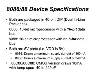
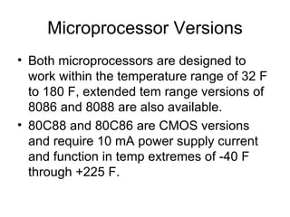
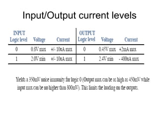
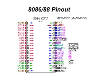
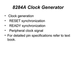
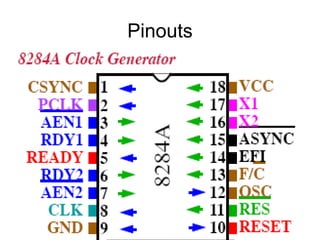
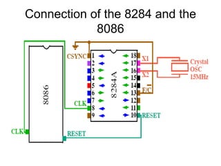
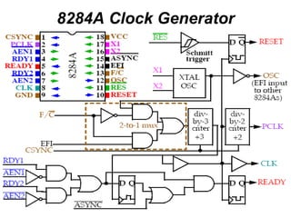
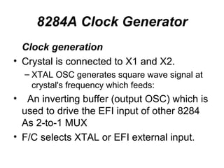
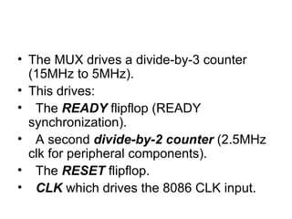
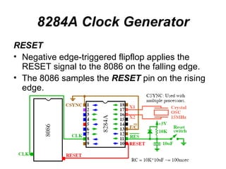
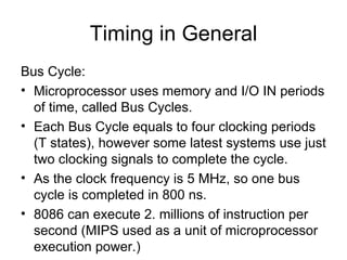
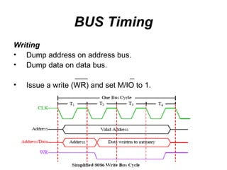
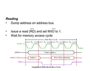
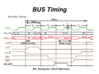
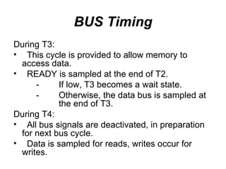
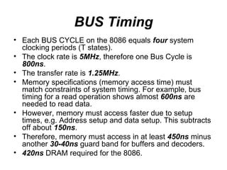
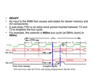
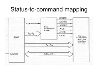
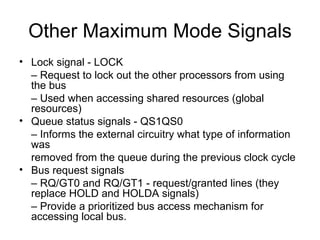
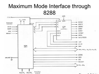
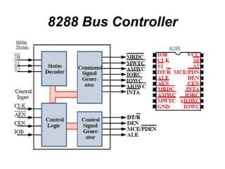
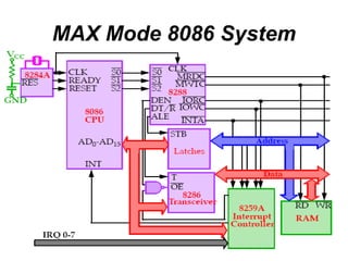
Microprocessor Systems EE351 8086 Chipset Badar-ul-Islam Department of Electrical Engineering NFC-IEFR [email_address]
8086/88 Device Specifications Both are packaged in 40-pin DIP (Dual In-Line Packages) 8086: 16-bit microprocessor with a  16-bit  data bus 8088: 16-bit microprocessor with an  8-bit  data bus Both are 5V parts (i.e. VDD is 5V) 8086: Draws a maximum supply current of 360mA 8088: Draws a maximum supply current of 340mA 80C86/80C88: CMOS version draws 10mA with temp spec -40 to 225oF
Microprocessor Versions Both microprocessors are designed to work within the temperature range of 32 F to 180 F, extended tem range versions of 8086 and 8088 are also available. 80C88 and 80C86 are CMOS versions and require 10 mA power supply current and function in temp extremes of -40 F through +225 F.
Input/Output current levels
I/O Characteristics Noise immunity is the difference between the logic 0 output voltage and logic 0 input voltage. It is recommended to connect no more than ten loads or combinations of load of any kind to any output without involving buffers, otherwise the increased noise may cause problems in the timing and synchronizing mechanisms.
8086/88 Pinout
8086/88 Pinout AD15-AD0 Multiplexed lines, address memory or some I/O port when ALE=1 and will be used as data bus when ALE=0.They will remain in high impedance state during hold acknowledge.AD0-AD7 in 8088 and AD0-AD15 in 8086. In 8088 processor A8-A15 pins are used as address bus only( as 8086 has address and data bus width of 16 bits and 8088 has an address bus of 16 lines and data bus of 8 lines only)
8086/88 Pinout A19/S6-A16/S3 (status/address bus,  multiplexed) High order 4 bits of the 20-bit address OR status bits S6-S3. S3 and S4 are used to select any one of the four memory segments (shown in a table). They attain a high impedance during hold acknowledge. __  __ M/IO or IO/M __  _ The IO/M (8088) and M/IO (8086) indicates if address is a Memory or IO address. Attain a high impedance state during hold acknowledge.
8086/88 Pinout ___ RD (Active Low) When 0, data bus is driven by memory or an I/O device and becomes receptive to data from memory or IO connected to the system. Attains high impedance during hold acknowledge. ___ WR  (Active Low) Microprocessor is driving data bus to memory or an I/O device and uP outputs data for memory or IO when this pin is low, data bus contains valid data for memory and IO device. This pin floats to high impedance during hold acknowledge.
8086/88 Pinout ALE  (Address latch enable) When 1, address data bus contains a memory or I/O address, otherwise it contains data. ALE signal does’t float during hold acknowledge. __ DT/R  (Data Transmit/Receive) This signal shows either Data bus is transmitting (if high) or receiving (if low) data. The signal is used to enable the external data bus buffers. DEN  (Data bus Enable) Activates external data bus buffers.
8086/88 Pinout INTR When 1 and IF=1(IF flag bit indicated by S5 status pin), microprocessor prepares to service a hardware interrupt. In this condition uP enters in an interrupt acknowledge cycle and INTA becomes active after current instruction completes. --------- INTA Interrupt Acknowledge generated by the microprocessor in response to INTR. Causes the interrupt vector to be put onto the data bus. NMI Non-maskable interrupt. Similar to INTR except IF flag bit is not consulted and interrupt is vector 2.
Interrupt Vectors It is a 4 byte number stored in first 1024 bytes of the memory when the processor operates in real mode, in the protected mode vector table is replaced by an interrupt descriptive table. There are 256 different interrupt vectors each vector contains the address of an interrupt service procedure. Each vector contains a value for IP and CS that forms the address of interrupt service procedure. Try to explore more on interrupt vectors.
8086/88 Pinout CLK Clock input must have a duty cycle of 33% (high for 1/3 of the cycle and low for 2/3 of the cycle to ensure proper internal timing) VCC/GND Power supply (+5V plus-minus 10%) and GND (0V) provides the return path for the supply, both processors have two ground pins and both must be connected to ground properly. MN/MX Select minimum (5V) or maximum mode (0V) of operation.
8086/88 Pinout
8086/88 Pinout ____  BHE/S7 Bus High Enable. Enables the most significant data bus bits (D15-D8) during a read or write operation. The state of S7 is always a logic 1. READY Used to insert wait states (controlled by memory and IO for reads/writes) into the microprocessor. If the ready input pin is placed at logic 0, the uP enters in a wait state and becomes idle. If this pin is placed at logic 1, the operation of the uP remains normal. RESET Microprocessor resets if this pin is held high for 4 clock periods. Instruction execution begins at FFFF0H and IF flag is cleared, so the future interrupts are disabled. TEST An input that is tested by the WAIT instruction. Commonly connected to the 8087 coprocessor.
8086/88 Pinout HOLD Requests a direct memory access (DMA). When 1, microprocessor stops and places address, data and control bus in high-impedance state. When 0, microprocessor executes the program instructions normally. HLDA  (Hold Acknowledge) Indicates that the microprocessor has entered the hold state.
8086/88 Pinout RO/GT1  and  RO/GT0 Request/grant pins request/grant direct memory accesses (DMA) during maximum mode operation. LOCK Lock output is used to lock peripherals off the system. Activated by using the LOCK: prefix on any instruction. QS1 and QS0 The queue status bits show status of internal instruction queue. Provided for access by the numeric coprocessor (8087).
8284A Clock Generator Clock generation RESET synchronization READY synchronization Peripheral clock signal For detailed pin specifications refer to text book.
Pinouts
Connection of the 8284 and the 8086
8284A Clock Generator
8284A Clock Generator Clock generation Crystal is connected to X1 and X2. XTAL OSC generates square wave signal at crystal's frequency which feeds: An inverting buffer (output OSC) which is used to drive the EFI input of other 8284 As 2-to-1 MUX F/C selects XTAL or EFI external input.
The MUX drives a divide-by-3 counter (15MHz to 5MHz). This drives: The  READY  flipflop (READY synchronization). A second  divide-by-2 counter  (2.5MHz clk for peripheral components). The  RESET  flipflop. CLK  which drives the 8086 CLK input.
8284A Clock Generator RESET Negative edge-triggered flipflop applies the RESET signal to the 8086 on the falling edge. The 8086 samples the  RESET  pin on the rising edge.
8284A Clock Generator Correct reset timing requires that the  RESET  input to the microprocessor becomes a logic 1  NO LATER  than 4 clocks after power up and stay high for at least 50µs.
BUS Buffering and Latching Computer systems have three buses Address Data Control The Address and Data bus are  multiplexed (shared)  due to pin limitations on the 8086. The ALE pin is used to control a set of latches.
BUS Buffering and Latching All signals MUST be buffered Buffered Latches for A0-A15. Control and A16-A19 +  BHE  are buffered separately. Data bus buffers must be bi-directional buffers. In a 8086 system, the memory is designed with two banks. High bank contains the higher order 8-bits and low bank the lower order 8-bits Data can be transferred as 8 bits from either bank or 16-bits from both BHE  pin selects the high-order memory bank
BUS Buffering and Latching
Timing in General Bus Cycle: Microprocessor uses memory and I/O IN periods of time, called Bus Cycles. Each Bus Cycle equals to four clocking periods (T states), however some latest systems use just two clocking signals to complete the cycle. As the clock frequency is 5 MHz, so one bus cycle is completed in 800 ns. 8086 can execute 2. millions of instruction per second (MIPS used as a unit of microprocessor execution power.)
BUS Timing Writing Dump address on address bus. Dump data on data bus. ___  _ Issue a write (WR) and set M/IO to 1.
Reading Dump address on address bus. __  __ Issue a read (RD) and set M/IO to 1. Wait for memory access cycle
BUS Timing
BUS Timing During T1: The address is placed on the Address/Data bus. Control signals M/IO, ALE and DT/R specify memory or I/O, latch the address onto the address bus and set the direction of data transfer on data bus. During T2: 8086 issues the RD or WR signal, DEN, and, for a write, the data. DEN enables the memory or I/O device to receive the data for writes and the 8086 to receive the data for reads.
BUS Timing During T3: This cycle is provided to allow memory to access data. READY is sampled at the end of T2. - If low, T3 becomes a wait state. - Otherwise, the data bus is sampled at  the end of T3. During T4: All bus signals are deactivated, in preparation for next bus cycle. Data is sampled for reads, writes occur for writes.
BUS Timing Each BUS CYCLE on the 8086 equals  four  system clocking periods (T states). The clock rate is  5MHz , therefore one Bus Cycle is  800ns . The transfer rate is  1.25MHz . Memory specifications (memory access time) must match constraints of system timing. For example, bus timing for a read operation shows almost  600ns  are needed to read data. However, memory must access faster due to setup times, e.g. Address setup and data setup. This subtracts off about  150ns . Therefore, memory must access in at least  450ns  minus another  30-40ns  guard band for buffers and decoders. 420ns  DRAM required for the 8086.
READY An input to the 8086 that causes wait states for slower memory and I/O components. A wait state (TW) is an extra clock period inserted between T2 and T3 to lengthen the bus cycle. For example, this extends a  460ns  bus cycle (at 5MHz clock) to  660ns .
Selection input MN/MX •  Minimum-mode/Maximum mode –  Min-mode: •  Used for simple or single processor systems •  Microprocessor provides all control signals –  Max-mode: •  Used for complex or multi-processor systems •  Microprocessor produces signals for implementing a multiprocessor/coprocessor system environment
Minimum mode (uniprocessor) 8088/8086 provides control signals implementing memory and I/O interfaces Signal groups: – Address/data bus – Control signals – Interrupt signals – Status signals – DMA signals
Signal Interfacing
Maximum-Mode Interface Used to produce signals for implementing a multiprocessor/coprocessor system environment –  There are several processors in the system environment –  They share common resources (called global resources) –  Each processor may have its local or private resources •  For multiprocessor systems--facilities are needed for implementing allocations of global resources and passing bus control to other microprocessors sharing the system bus.
MIN and MAX Mode Controlled through the  MN/MX  pin. Minimum mode  is cheaper since all control signals for memory and I/O are generated by the microprocessor. Maximum mode  is designed to be used when a coprocessor (8087) exists in the system.
MIN and MAX Mode Some of the control signals must be generated externally, due to redefinition of certain control pins on the 8086. The following pins are lost when the 8086 operates in  Maximum mode . ALE WR IO/M DT/R DEN INTA This requires an external bus controller:  8288 Bus Controller .
8288 Bus Controller Provides signals that are required to control the memory, I/O, and interrupt interfaces. Connects directly to 8088/8086. –  Processor pins S0,S1,S2 carries a status code  provided prior to initiation of each bus cycle –  Bus controller generates appropriately timed command and control signals in response.
Signals of the 8288 Memory signals MRDC - memory read command MWTC - memory write command AMWC - advanced memory write command –  I/O signals IORC - I/O read command IOWC - I/O write command AIOWC - advanced I/O write command –  Interrupt signals INTA - interrupt acknowledge –  Other signals DEN, DT/R, and ALE  (the same as for the minimum-mode system)
Status-to-command mapping
Other Maximum Mode Signals Lock signal - LOCK –  Request to lock out the other processors from using the bus –  Used when accessing shared resources (global resources) Queue status signals - QS1QS0 –  Informs the external circuitry what type of information was removed from the queue during the previous clock cycle Bus request signals –  RQ/GT0 and RQ/GT1 - request/granted lines (they replace HOLD and HOLDA signals) –  Provide a prioritized bus access mechanism for accessing local bus.
Maximum Mode Interface through 8288
8288 Bus Controller
8288 Bus Controller Separate signals are used for I/O (IORC and IOWC) and memory (MRDC and MWTC). Also provided are advanced memory (AIOWC) and I/O (AIOWC) write strobes plus INTA.
MAX Mode 8086 System

Lect 5

  • 1.
    Microprocessor Systems EE3518086 Chipset Badar-ul-Islam Department of Electrical Engineering NFC-IEFR [email_address]
  • 2.
    8086/88 Device SpecificationsBoth are packaged in 40-pin DIP (Dual In-Line Packages) 8086: 16-bit microprocessor with a 16-bit data bus 8088: 16-bit microprocessor with an 8-bit data bus Both are 5V parts (i.e. VDD is 5V) 8086: Draws a maximum supply current of 360mA 8088: Draws a maximum supply current of 340mA 80C86/80C88: CMOS version draws 10mA with temp spec -40 to 225oF
  • 3.
    Microprocessor Versions Bothmicroprocessors are designed to work within the temperature range of 32 F to 180 F, extended tem range versions of 8086 and 8088 are also available. 80C88 and 80C86 are CMOS versions and require 10 mA power supply current and function in temp extremes of -40 F through +225 F.
  • 4.
  • 5.
    I/O Characteristics Noiseimmunity is the difference between the logic 0 output voltage and logic 0 input voltage. It is recommended to connect no more than ten loads or combinations of load of any kind to any output without involving buffers, otherwise the increased noise may cause problems in the timing and synchronizing mechanisms.
  • 6.
  • 7.
    8086/88 Pinout AD15-AD0Multiplexed lines, address memory or some I/O port when ALE=1 and will be used as data bus when ALE=0.They will remain in high impedance state during hold acknowledge.AD0-AD7 in 8088 and AD0-AD15 in 8086. In 8088 processor A8-A15 pins are used as address bus only( as 8086 has address and data bus width of 16 bits and 8088 has an address bus of 16 lines and data bus of 8 lines only)
  • 8.
    8086/88 Pinout A19/S6-A16/S3(status/address bus, multiplexed) High order 4 bits of the 20-bit address OR status bits S6-S3. S3 and S4 are used to select any one of the four memory segments (shown in a table). They attain a high impedance during hold acknowledge. __ __ M/IO or IO/M __ _ The IO/M (8088) and M/IO (8086) indicates if address is a Memory or IO address. Attain a high impedance state during hold acknowledge.
  • 9.
    8086/88 Pinout ___RD (Active Low) When 0, data bus is driven by memory or an I/O device and becomes receptive to data from memory or IO connected to the system. Attains high impedance during hold acknowledge. ___ WR (Active Low) Microprocessor is driving data bus to memory or an I/O device and uP outputs data for memory or IO when this pin is low, data bus contains valid data for memory and IO device. This pin floats to high impedance during hold acknowledge.
  • 10.
    8086/88 Pinout ALE (Address latch enable) When 1, address data bus contains a memory or I/O address, otherwise it contains data. ALE signal does’t float during hold acknowledge. __ DT/R (Data Transmit/Receive) This signal shows either Data bus is transmitting (if high) or receiving (if low) data. The signal is used to enable the external data bus buffers. DEN (Data bus Enable) Activates external data bus buffers.
  • 11.
    8086/88 Pinout INTRWhen 1 and IF=1(IF flag bit indicated by S5 status pin), microprocessor prepares to service a hardware interrupt. In this condition uP enters in an interrupt acknowledge cycle and INTA becomes active after current instruction completes. --------- INTA Interrupt Acknowledge generated by the microprocessor in response to INTR. Causes the interrupt vector to be put onto the data bus. NMI Non-maskable interrupt. Similar to INTR except IF flag bit is not consulted and interrupt is vector 2.
  • 12.
    Interrupt Vectors Itis a 4 byte number stored in first 1024 bytes of the memory when the processor operates in real mode, in the protected mode vector table is replaced by an interrupt descriptive table. There are 256 different interrupt vectors each vector contains the address of an interrupt service procedure. Each vector contains a value for IP and CS that forms the address of interrupt service procedure. Try to explore more on interrupt vectors.
  • 13.
    8086/88 Pinout CLKClock input must have a duty cycle of 33% (high for 1/3 of the cycle and low for 2/3 of the cycle to ensure proper internal timing) VCC/GND Power supply (+5V plus-minus 10%) and GND (0V) provides the return path for the supply, both processors have two ground pins and both must be connected to ground properly. MN/MX Select minimum (5V) or maximum mode (0V) of operation.
  • 14.
  • 15.
    8086/88 Pinout ____ BHE/S7 Bus High Enable. Enables the most significant data bus bits (D15-D8) during a read or write operation. The state of S7 is always a logic 1. READY Used to insert wait states (controlled by memory and IO for reads/writes) into the microprocessor. If the ready input pin is placed at logic 0, the uP enters in a wait state and becomes idle. If this pin is placed at logic 1, the operation of the uP remains normal. RESET Microprocessor resets if this pin is held high for 4 clock periods. Instruction execution begins at FFFF0H and IF flag is cleared, so the future interrupts are disabled. TEST An input that is tested by the WAIT instruction. Commonly connected to the 8087 coprocessor.
  • 16.
    8086/88 Pinout HOLDRequests a direct memory access (DMA). When 1, microprocessor stops and places address, data and control bus in high-impedance state. When 0, microprocessor executes the program instructions normally. HLDA (Hold Acknowledge) Indicates that the microprocessor has entered the hold state.
  • 17.
    8086/88 Pinout RO/GT1 and RO/GT0 Request/grant pins request/grant direct memory accesses (DMA) during maximum mode operation. LOCK Lock output is used to lock peripherals off the system. Activated by using the LOCK: prefix on any instruction. QS1 and QS0 The queue status bits show status of internal instruction queue. Provided for access by the numeric coprocessor (8087).
  • 18.
    8284A Clock GeneratorClock generation RESET synchronization READY synchronization Peripheral clock signal For detailed pin specifications refer to text book.
  • 19.
  • 20.
    Connection of the8284 and the 8086
  • 21.
  • 22.
    8284A Clock GeneratorClock generation Crystal is connected to X1 and X2. XTAL OSC generates square wave signal at crystal's frequency which feeds: An inverting buffer (output OSC) which is used to drive the EFI input of other 8284 As 2-to-1 MUX F/C selects XTAL or EFI external input.
  • 23.
    The MUX drivesa divide-by-3 counter (15MHz to 5MHz). This drives: The READY flipflop (READY synchronization). A second divide-by-2 counter (2.5MHz clk for peripheral components). The RESET flipflop. CLK which drives the 8086 CLK input.
  • 24.
    8284A Clock GeneratorRESET Negative edge-triggered flipflop applies the RESET signal to the 8086 on the falling edge. The 8086 samples the RESET pin on the rising edge.
  • 25.
    8284A Clock GeneratorCorrect reset timing requires that the RESET input to the microprocessor becomes a logic 1 NO LATER than 4 clocks after power up and stay high for at least 50µs.
  • 26.
    BUS Buffering andLatching Computer systems have three buses Address Data Control The Address and Data bus are multiplexed (shared) due to pin limitations on the 8086. The ALE pin is used to control a set of latches.
  • 27.
    BUS Buffering andLatching All signals MUST be buffered Buffered Latches for A0-A15. Control and A16-A19 + BHE are buffered separately. Data bus buffers must be bi-directional buffers. In a 8086 system, the memory is designed with two banks. High bank contains the higher order 8-bits and low bank the lower order 8-bits Data can be transferred as 8 bits from either bank or 16-bits from both BHE pin selects the high-order memory bank
  • 28.
  • 29.
    Timing in GeneralBus Cycle: Microprocessor uses memory and I/O IN periods of time, called Bus Cycles. Each Bus Cycle equals to four clocking periods (T states), however some latest systems use just two clocking signals to complete the cycle. As the clock frequency is 5 MHz, so one bus cycle is completed in 800 ns. 8086 can execute 2. millions of instruction per second (MIPS used as a unit of microprocessor execution power.)
  • 30.
    BUS Timing WritingDump address on address bus. Dump data on data bus. ___ _ Issue a write (WR) and set M/IO to 1.
  • 31.
    Reading Dump addresson address bus. __ __ Issue a read (RD) and set M/IO to 1. Wait for memory access cycle
  • 32.
  • 33.
    BUS Timing DuringT1: The address is placed on the Address/Data bus. Control signals M/IO, ALE and DT/R specify memory or I/O, latch the address onto the address bus and set the direction of data transfer on data bus. During T2: 8086 issues the RD or WR signal, DEN, and, for a write, the data. DEN enables the memory or I/O device to receive the data for writes and the 8086 to receive the data for reads.
  • 34.
    BUS Timing DuringT3: This cycle is provided to allow memory to access data. READY is sampled at the end of T2. - If low, T3 becomes a wait state. - Otherwise, the data bus is sampled at the end of T3. During T4: All bus signals are deactivated, in preparation for next bus cycle. Data is sampled for reads, writes occur for writes.
  • 35.
    BUS Timing EachBUS CYCLE on the 8086 equals four system clocking periods (T states). The clock rate is 5MHz , therefore one Bus Cycle is 800ns . The transfer rate is 1.25MHz . Memory specifications (memory access time) must match constraints of system timing. For example, bus timing for a read operation shows almost 600ns are needed to read data. However, memory must access faster due to setup times, e.g. Address setup and data setup. This subtracts off about 150ns . Therefore, memory must access in at least 450ns minus another 30-40ns guard band for buffers and decoders. 420ns DRAM required for the 8086.
  • 36.
    READY An inputto the 8086 that causes wait states for slower memory and I/O components. A wait state (TW) is an extra clock period inserted between T2 and T3 to lengthen the bus cycle. For example, this extends a 460ns bus cycle (at 5MHz clock) to 660ns .
  • 37.
    Selection input MN/MX• Minimum-mode/Maximum mode – Min-mode: • Used for simple or single processor systems • Microprocessor provides all control signals – Max-mode: • Used for complex or multi-processor systems • Microprocessor produces signals for implementing a multiprocessor/coprocessor system environment
  • 38.
    Minimum mode (uniprocessor)8088/8086 provides control signals implementing memory and I/O interfaces Signal groups: – Address/data bus – Control signals – Interrupt signals – Status signals – DMA signals
  • 39.
  • 40.
    Maximum-Mode Interface Usedto produce signals for implementing a multiprocessor/coprocessor system environment – There are several processors in the system environment – They share common resources (called global resources) – Each processor may have its local or private resources • For multiprocessor systems--facilities are needed for implementing allocations of global resources and passing bus control to other microprocessors sharing the system bus.
  • 41.
    MIN and MAXMode Controlled through the MN/MX pin. Minimum mode is cheaper since all control signals for memory and I/O are generated by the microprocessor. Maximum mode is designed to be used when a coprocessor (8087) exists in the system.
  • 42.
    MIN and MAXMode Some of the control signals must be generated externally, due to redefinition of certain control pins on the 8086. The following pins are lost when the 8086 operates in Maximum mode . ALE WR IO/M DT/R DEN INTA This requires an external bus controller: 8288 Bus Controller .
  • 43.
    8288 Bus ControllerProvides signals that are required to control the memory, I/O, and interrupt interfaces. Connects directly to 8088/8086. – Processor pins S0,S1,S2 carries a status code provided prior to initiation of each bus cycle – Bus controller generates appropriately timed command and control signals in response.
  • 44.
    Signals of the8288 Memory signals MRDC - memory read command MWTC - memory write command AMWC - advanced memory write command – I/O signals IORC - I/O read command IOWC - I/O write command AIOWC - advanced I/O write command – Interrupt signals INTA - interrupt acknowledge – Other signals DEN, DT/R, and ALE (the same as for the minimum-mode system)
  • 45.
  • 46.
    Other Maximum ModeSignals Lock signal - LOCK – Request to lock out the other processors from using the bus – Used when accessing shared resources (global resources) Queue status signals - QS1QS0 – Informs the external circuitry what type of information was removed from the queue during the previous clock cycle Bus request signals – RQ/GT0 and RQ/GT1 - request/granted lines (they replace HOLD and HOLDA signals) – Provide a prioritized bus access mechanism for accessing local bus.
  • 47.
  • 48.
  • 49.
    8288 Bus ControllerSeparate signals are used for I/O (IORC and IOWC) and memory (MRDC and MWTC). Also provided are advanced memory (AIOWC) and I/O (AIOWC) write strobes plus INTA.
  • 50.