Downloaded 411 times


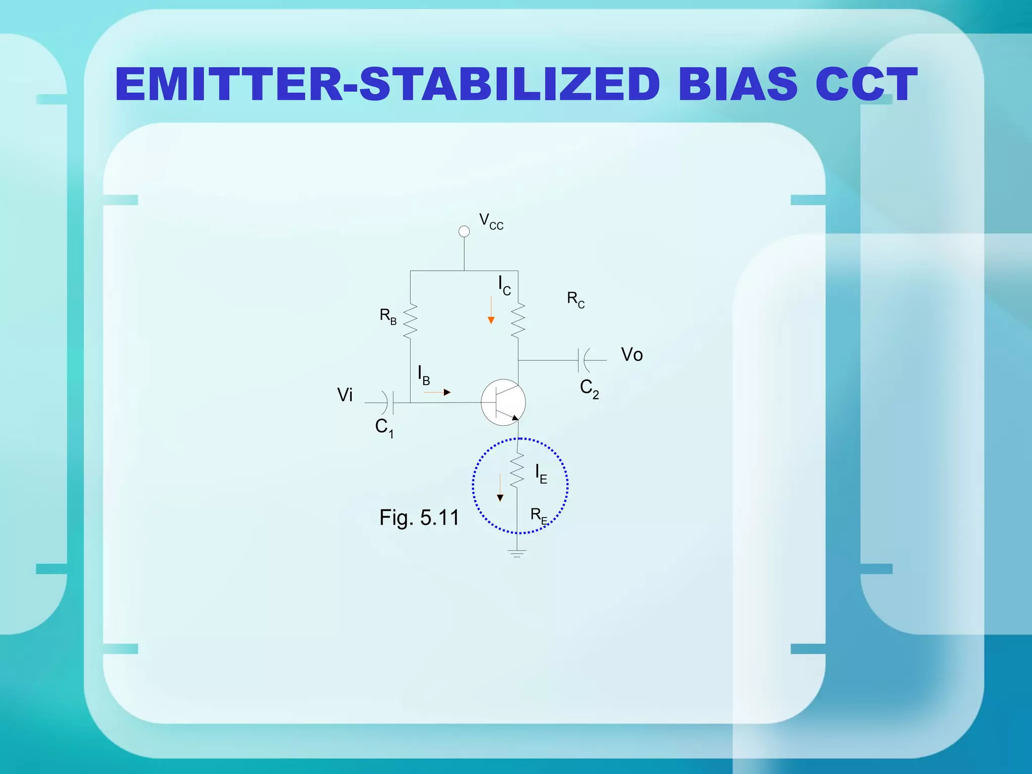
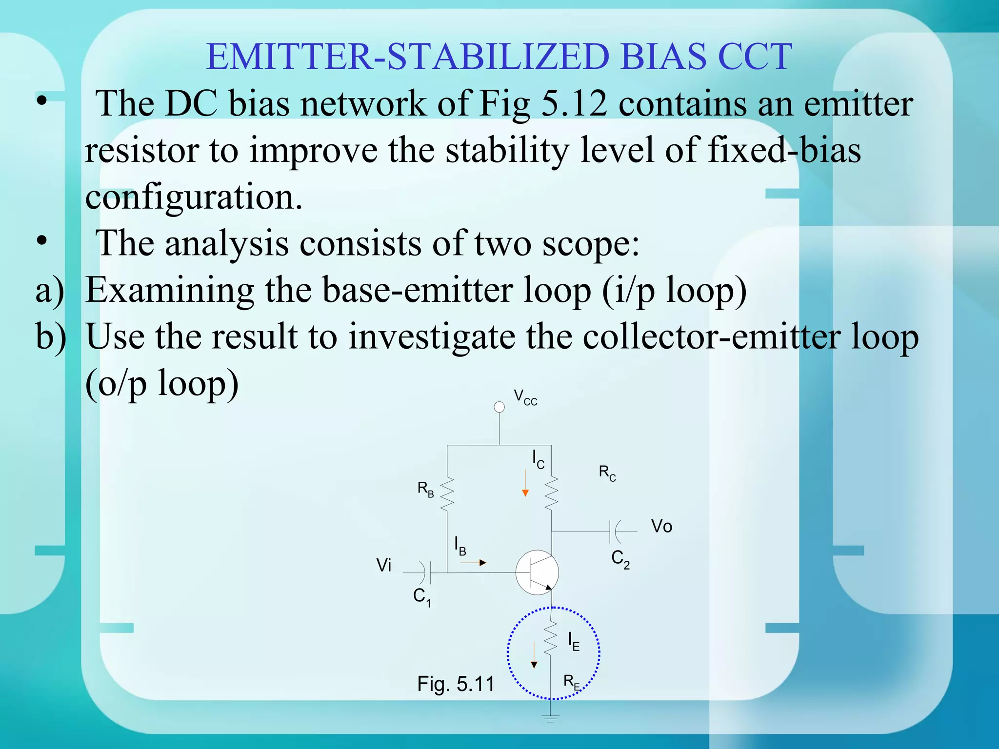
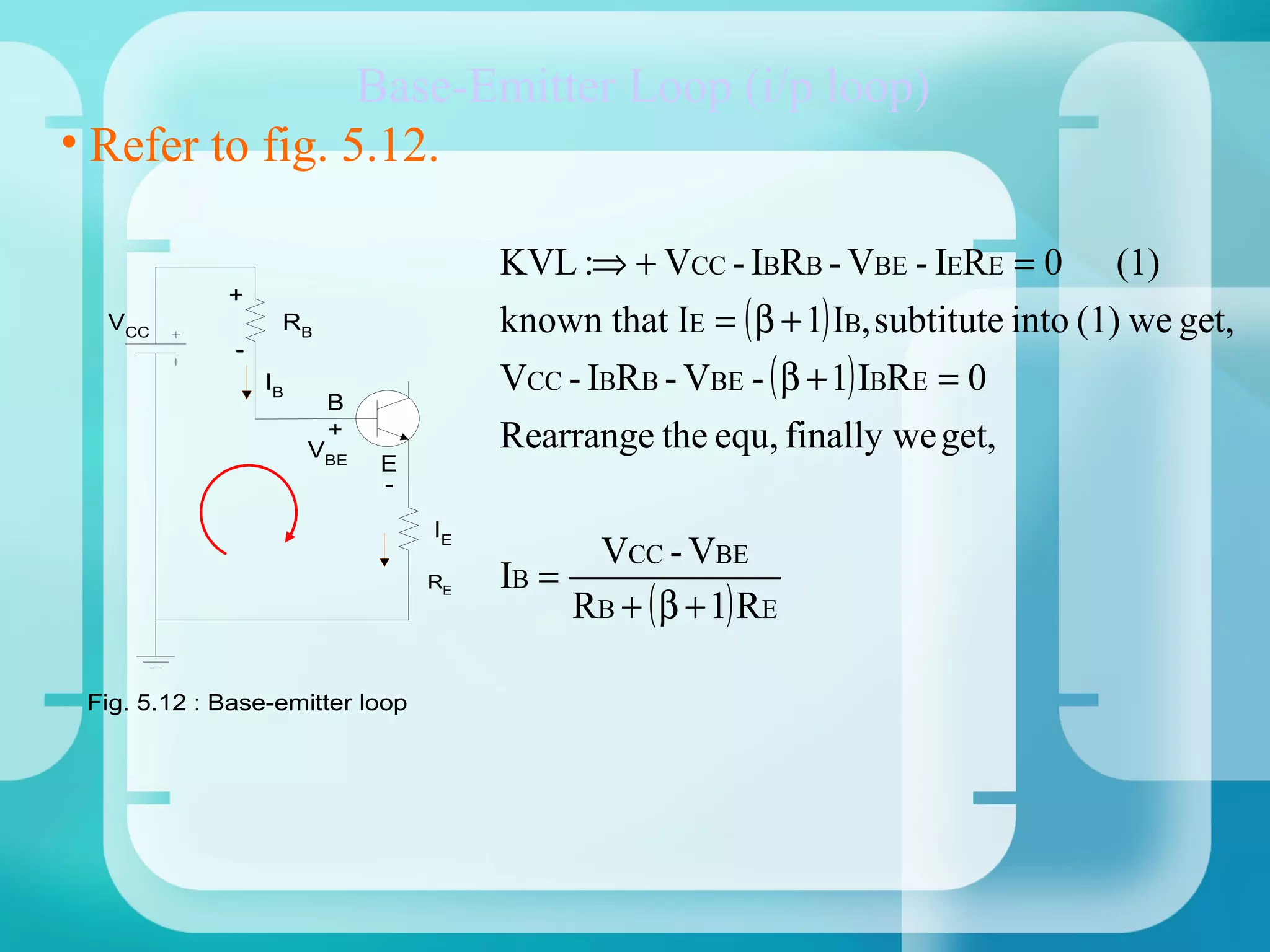
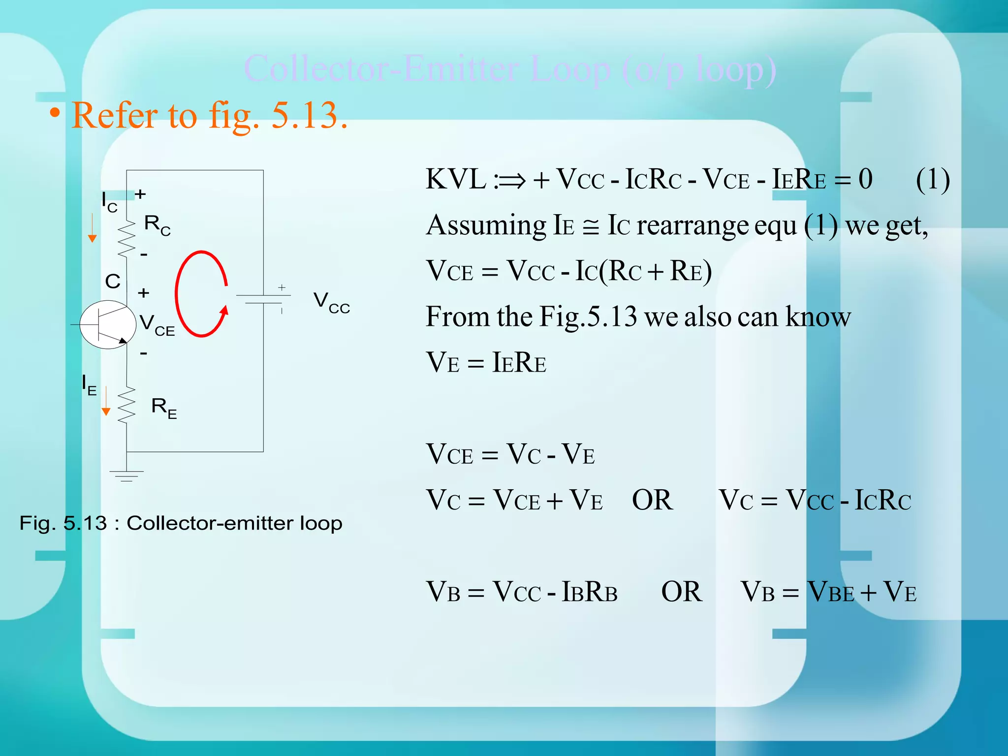

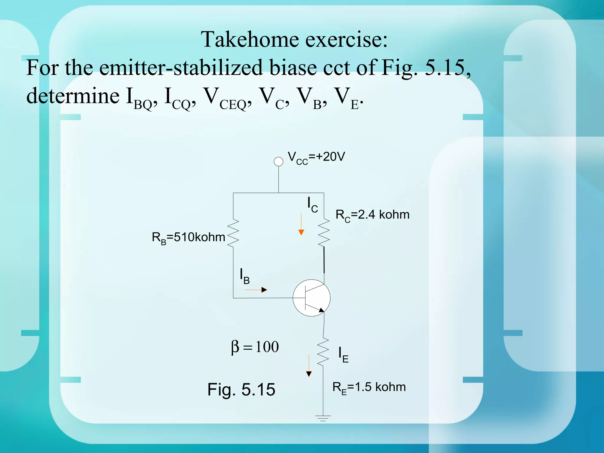


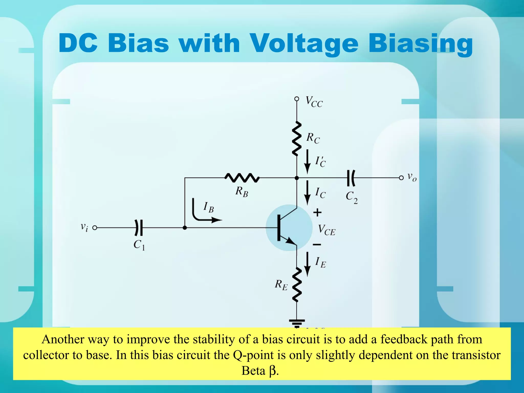
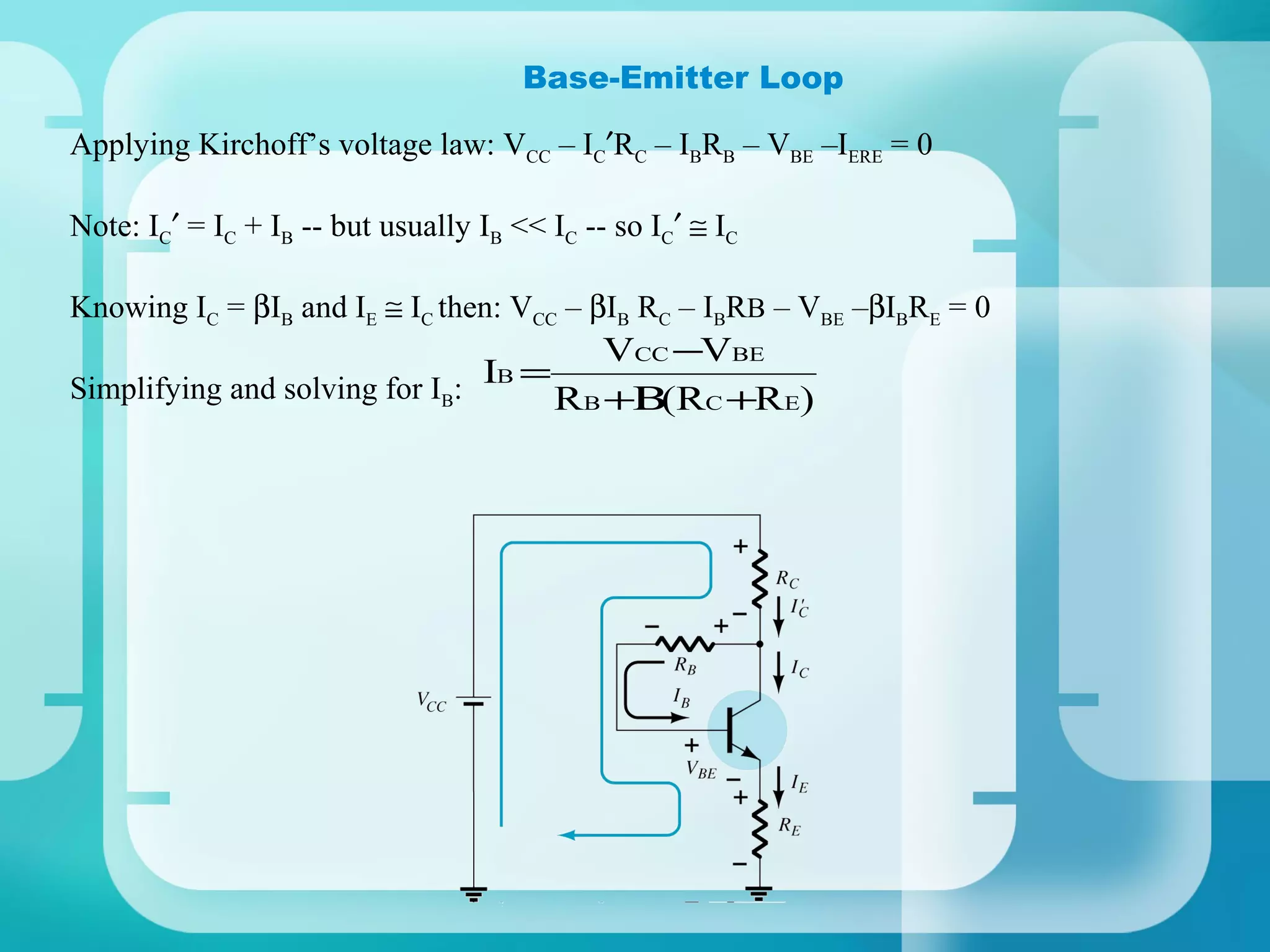
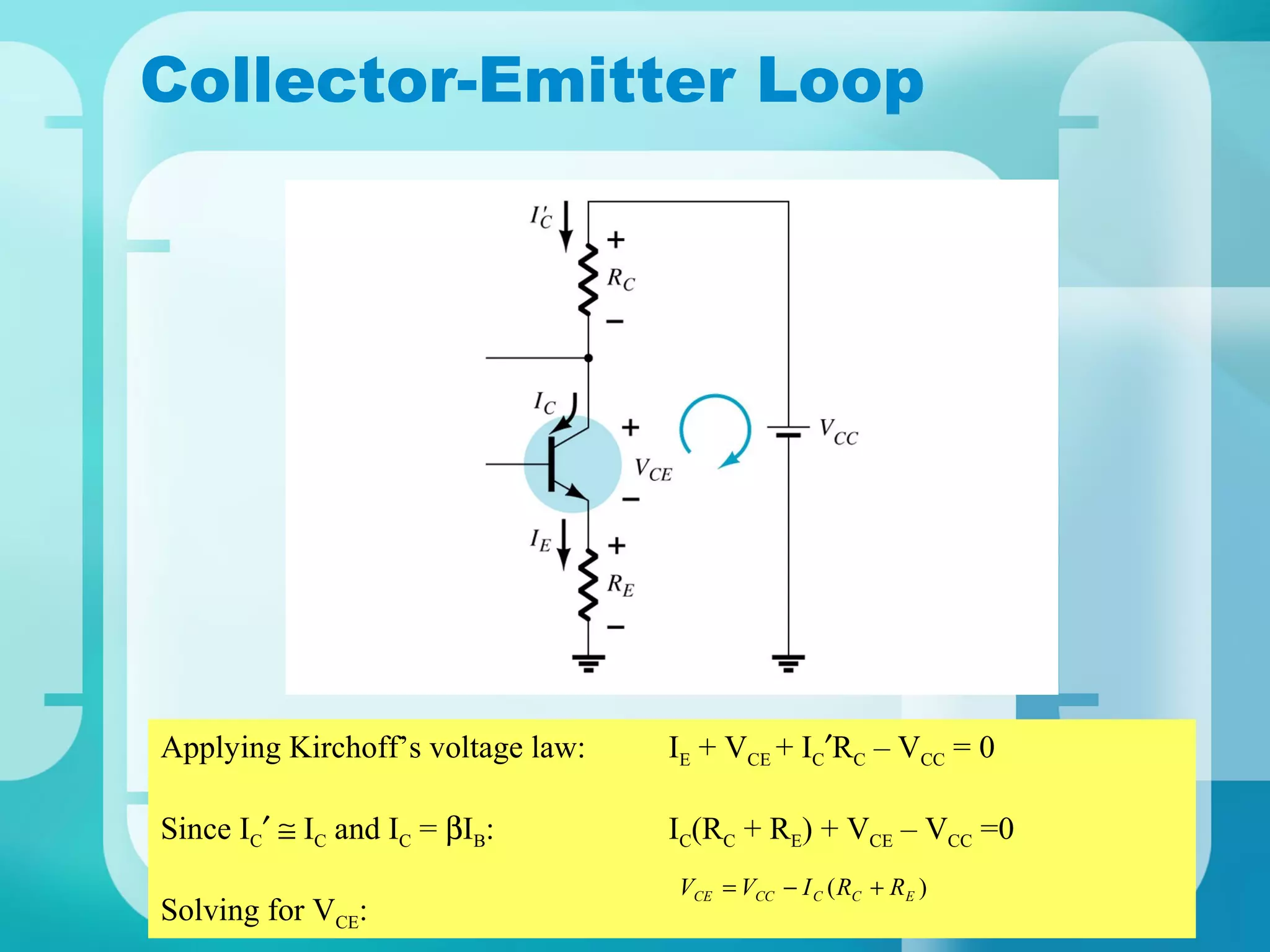


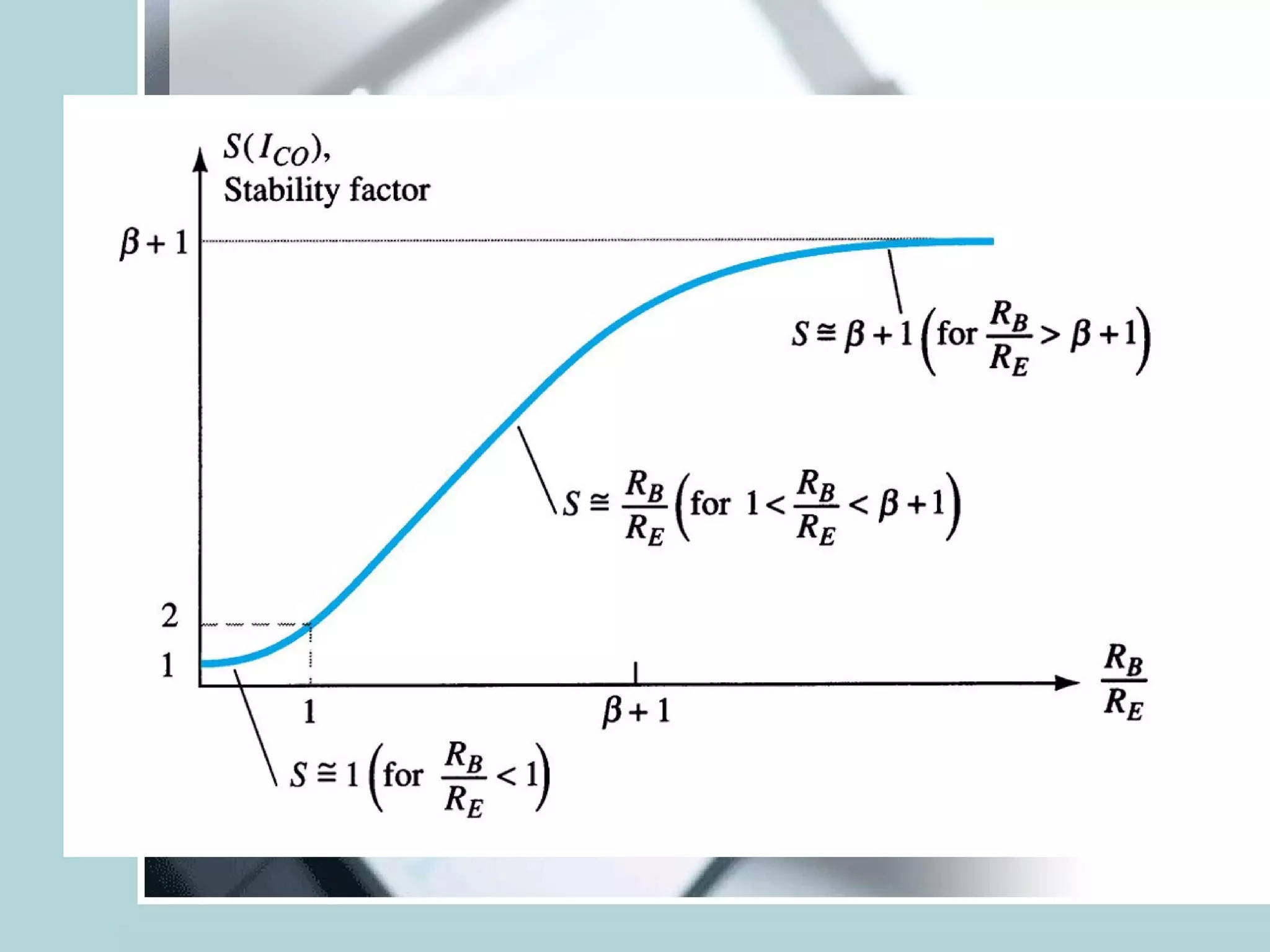


Here are the key steps to analyze the emitter-stabilized bias circuit: 1. Analyze the base-emitter loop using KVL: VCC - IBRE - VBE - IERE = 0 2. Solve for IB and substitute into IE = βIB 3. Analyze the collector-emitter loop using KVL: VCC - IC(RC + RE) - VCE = 0 4. Solve simultaneously with the base-emitter loop equation to find Q-point values of IB, IC, VBE, VCE. The addition of the emitter resistor RE provides negative feedback which helps stabilize the operating point against variations in β and temperature. This makes the


