Downloaded 24 times
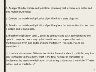
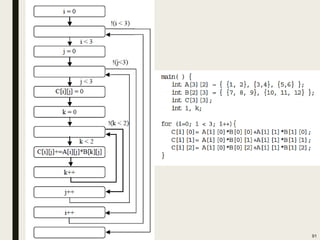
![main()
{
int A[3][2]={ {1, 2}, {3,4}, {5,6}};
int B[2][3]= {{7, 8, 9}, (10, 11, 12}};
int C[3][3], i, j, k;
for(i=0; i<3; i++) {
for(j=0; j<3; j++) {
c[i][j]=0;
for(k=0;k<2;k++){
c[i][j]+=A[i][k]*B[k][j];
}
}
}
}
90](https://image.slidesharecdn.com/esd-module2-181227161720/85/Esd-module2-90-320.jpg)
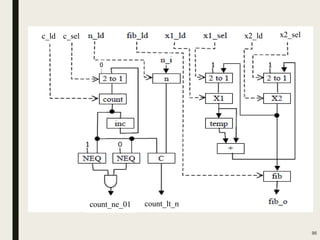

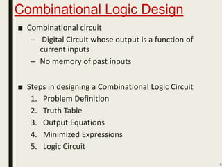
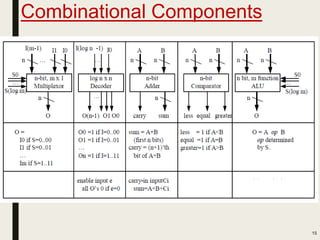
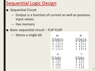
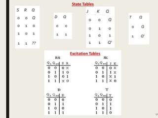
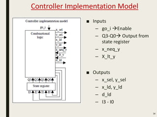
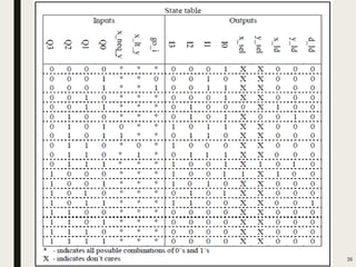
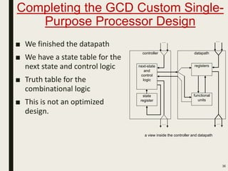
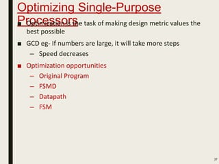
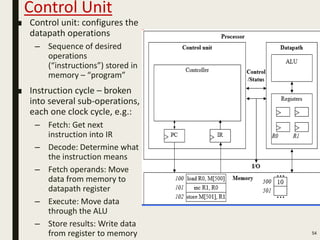
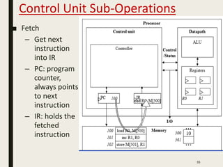
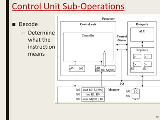
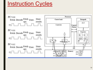
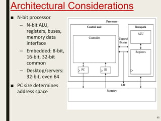
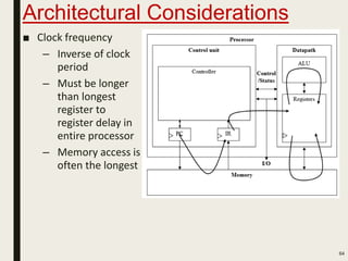
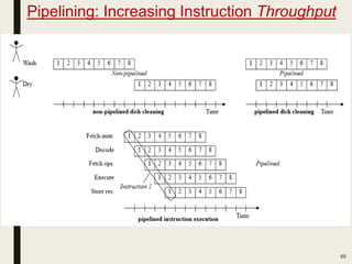
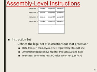
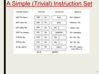
This document discusses processor design, including custom single-purpose processors and general-purpose processors. It covers topics such as combinational and sequential logic design, finite state machine design, optimizing custom processors by improving the original program, finite state machine with datapath, and datapath and finite state machine. General-purpose processors are also introduced, including their basic architecture consisting of a control unit and datapath.