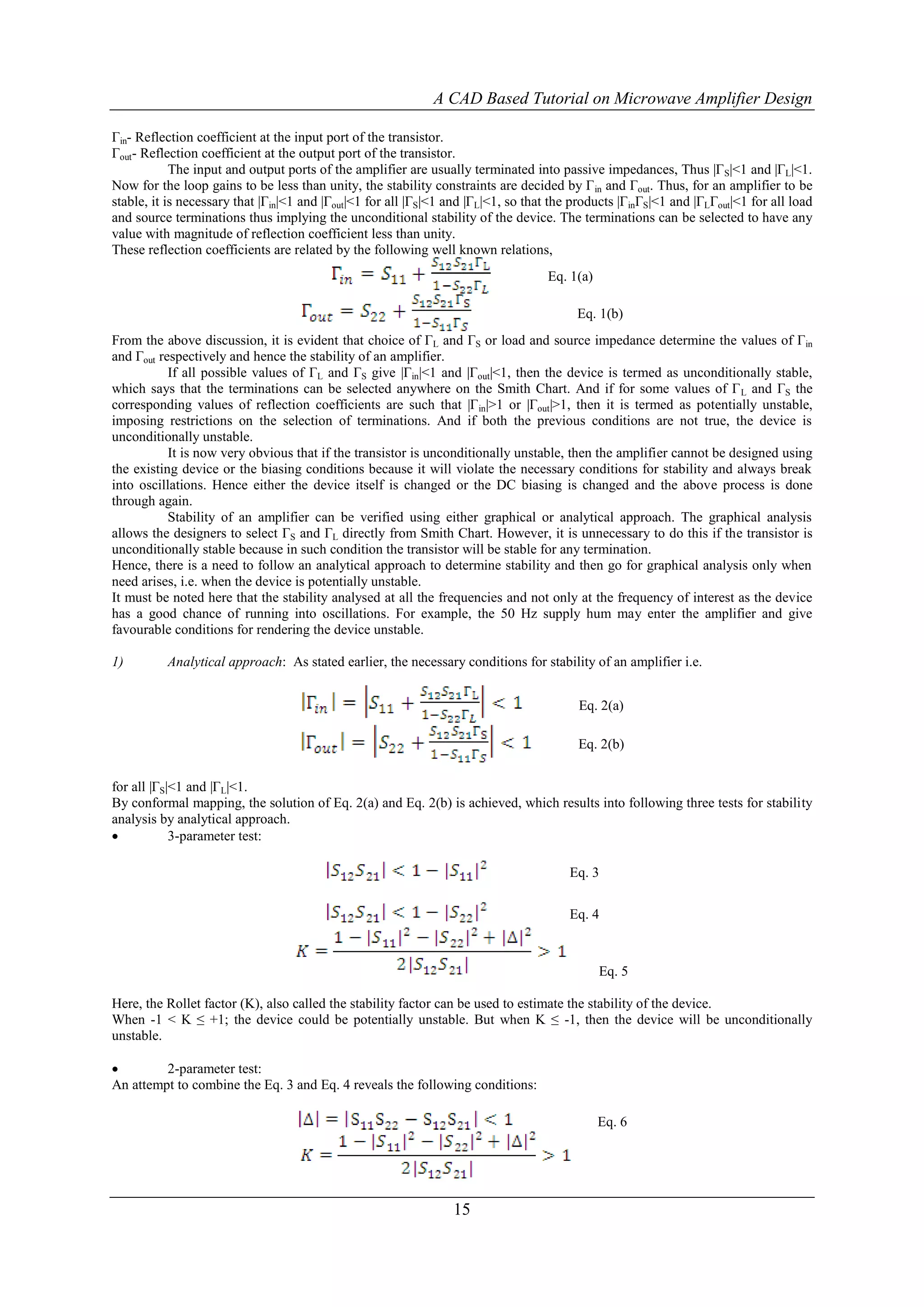
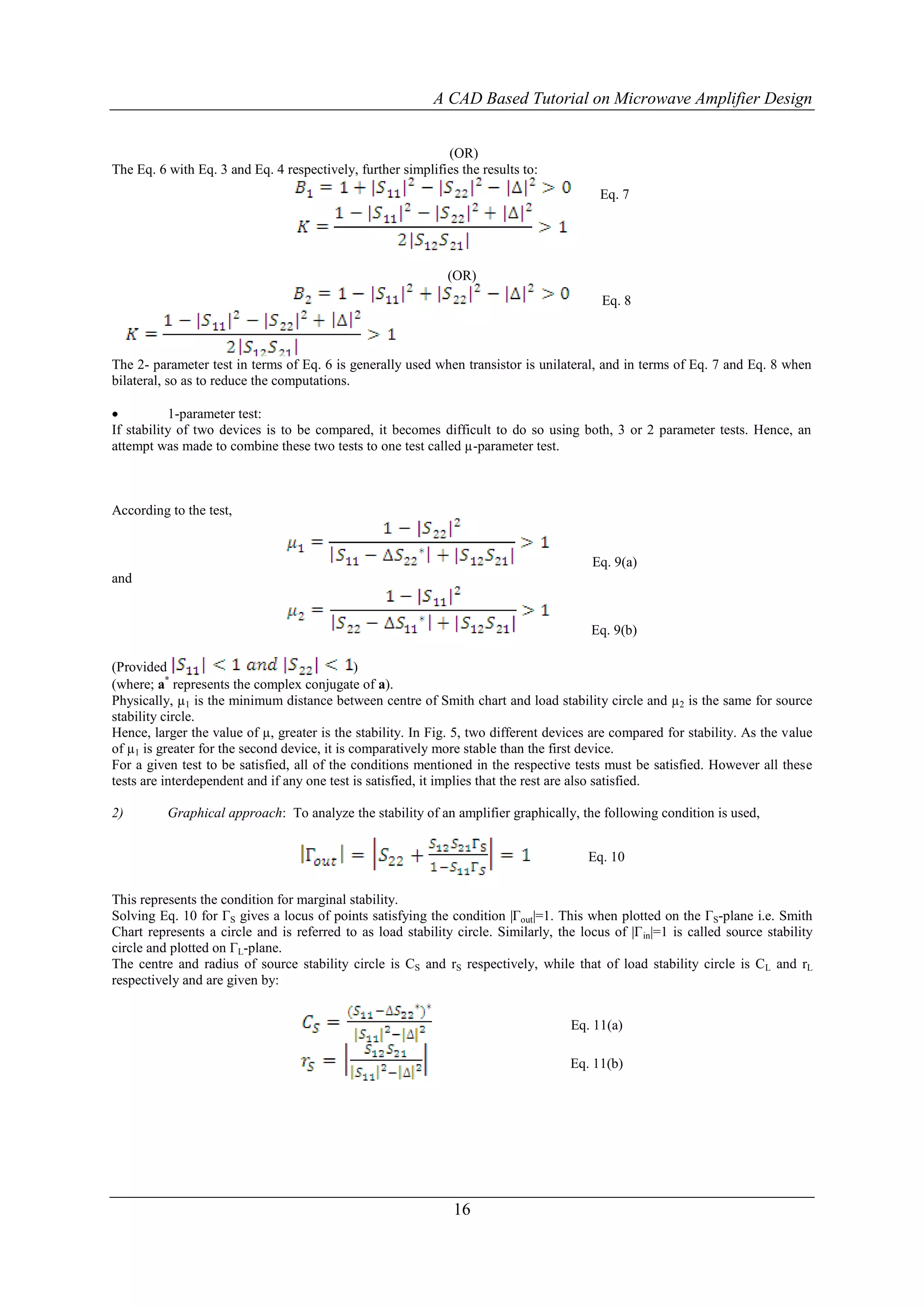
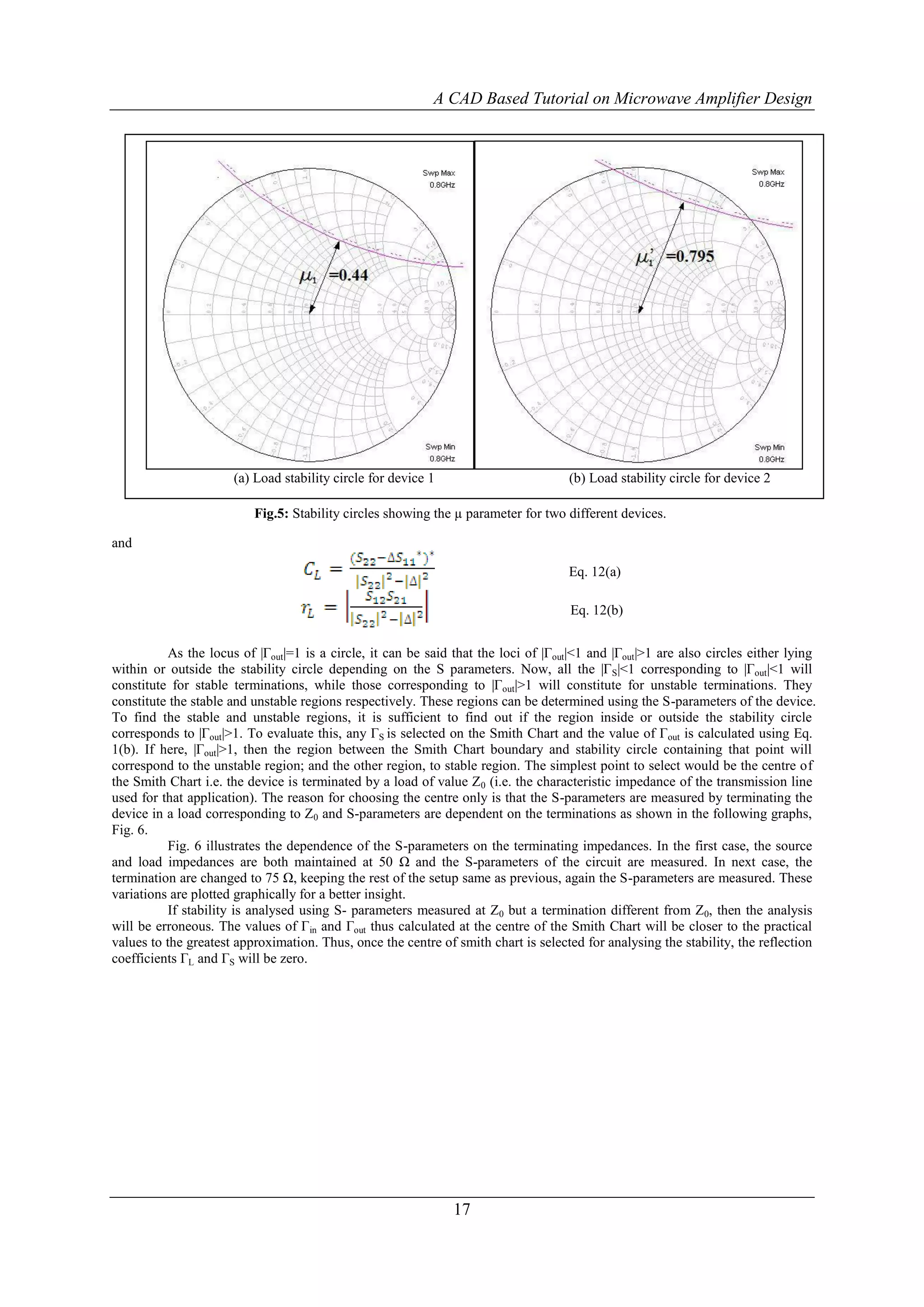
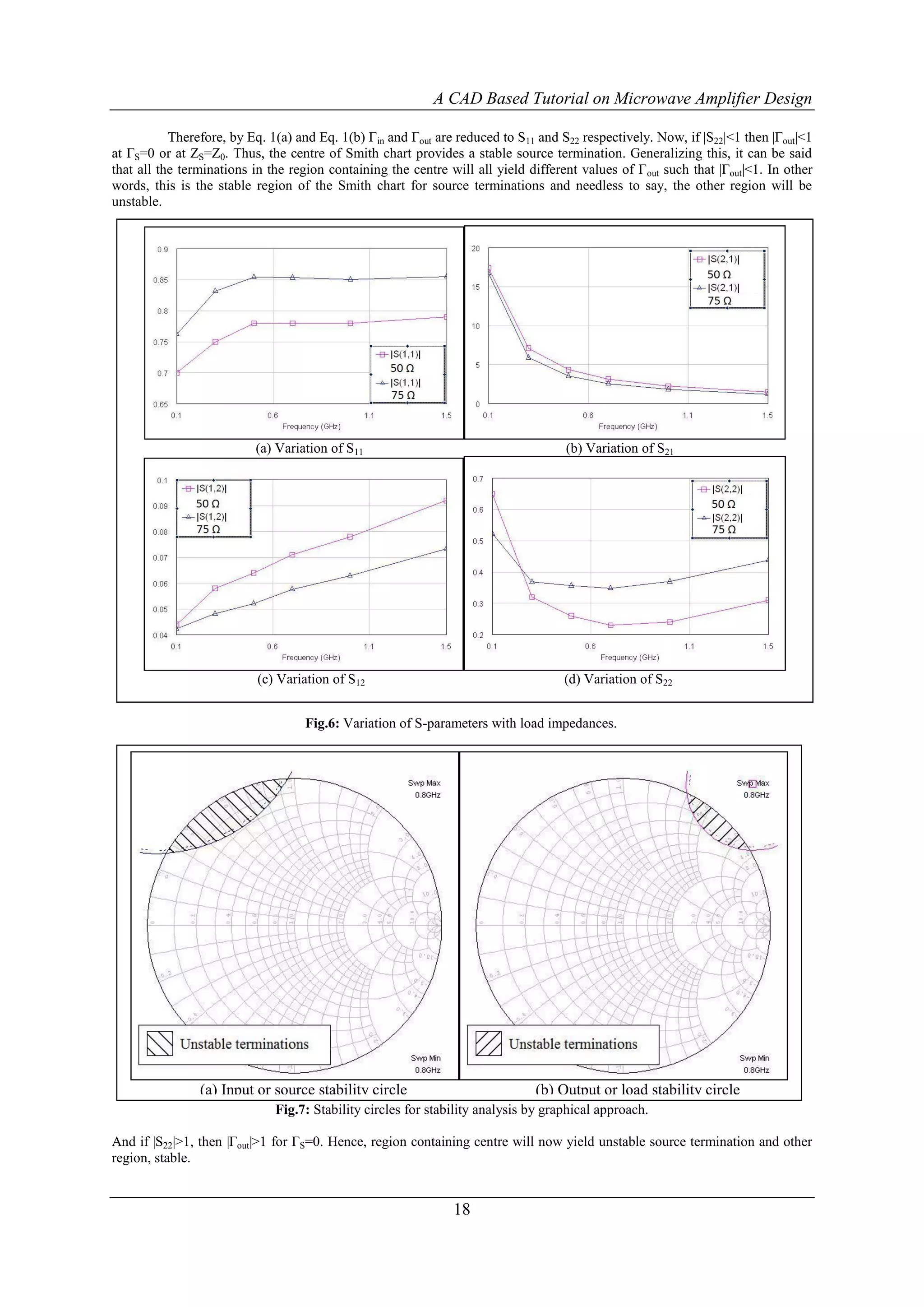
This document provides a tutorial on designing microwave amplifiers using CAD software. It discusses:
1) The key steps in microwave amplifier design including selecting an active device, biasing it, characterizing the device, analyzing stability, and implementing matching networks.
2) Methods for stability analysis including the Rollett K-factor test, source-load circle graphical analysis on the Smith Chart, and evaluating the reflection coefficients Γin and Γout.
3) How CAD tools like AWR's Microwave Office can be used to design microwave amplifiers by simulating the circuit and evaluating performance based on the device specifications and design parameters.
Qualitative Analysis of Darlington Feedback Amplifier at 45nm TechnologyjournalBEEI
The transistors are the key element of present communication system having high data rate. Some applications need high gain by using very low frequency, and then transistors are used. Amplifier is the key element in many applications of present high data rate communication system such as low noise amplifier (LNA), broadband amplifier, distributed and power amplifier. The Darlington pair amplifier is analyzed for high frequency performance and related effect of bandwidth. Broadband feedback Darlington pair amplifier is designed with enhanced gain, bandwidth and slew rate. This paper presents the comparison of single stage and three stage feedback Darlington feedback amplifier with reference to gain, bandwidth and slew rate. This paper is simulated on cadence analog design environment at GPDK 45nm technology. This paper shows that increase in gain, bandwidth and slew rate of three stage Darlington feedback amplifier can show better stability over the single stage Darlington feedback amplifier.
International Journal of Computational Engineering Research(IJCER)ijceronline
International Journal of Computational Engineering Research(IJCER) is an intentional online Journal in English monthly publishing journal. This Journal publish original research work that contributes significantly to further the scientific knowledge in engineering and Technology.
42 30 nA Comparative Study of Power Semiconductor Devices for Industrial PWM ...IAES-IJPEDS
The growing demand of energy translates into efficiency requirements of
energy conversion systems and electric drives. Both these systems are based
on Pulse Width Modulation (PWM) Inverter. In this paper we firstly present
the state of art of the main types of semiconductors devices for Industrial
PWM Inverter. In particular we examine the last generations of Silicon
Carbide (SiC) MOSFETs and Insulated Gate Bipolar Transistors (IGBTs)
and we present a comparison between these devices, obtained by SPICE
simulations, both for static characteristics at different temperatures and for
dynamic ones at different gate resistance, in order to identify the one which
makes the PWM inverter more efficient.
IJERA (International journal of Engineering Research and Applications) is International online, ... peer reviewed journal. For more detail or submit your article, please visit www.ijera.com
IOSR Journal of Electronics and Communication Engineering(IOSR-JECE) is an open access international journal that provides rapid publication (within a month) of articles in all areas of electronics and communication engineering and its applications. The journal welcomes publications of high quality papers on theoretical developments and practical applications in electronics and communication engineering. Original research papers, state-of-the-art reviews, and high quality technical notes are invited for publications.
a report on Off-line Fault Localization Technique on HVDC Submarine Cable via Time-Frequency Domain Reflectometry.
other fault tech like TDR, FDR included.
LOW POWER SI CLASS E POWER AMPLIFIER AND RF SWITCH FOR HEALTH CAREieijjournal
This research was to design a 2.4 GHz class E Power Amplifier (PA) for health care, with 0.18um
Semiconductor Manufacturing International Corporation CMOS technology by using Cadence software.
And also RF switch was designed at cadence software with power Jazz 180nm SOI process. The ultimate
goal for such application is to reach high performance and low cost, and between high performance and
low power consumption design. This paper introduces the design of a 2.4GHz class E power amplifier and RF switch design. PA consists of cascade stage with negative capacitance. This power amplifier can transmit 16dBm output power to a 50Ω load. The performance of the power amplifier and switch meet the specification requirements of the desired.
International Journal of Engineering Research and DevelopmentIJERD Editor
Electrical, Electronics and Computer Engineering,
Information Engineering and Technology,
Mechanical, Industrial and Manufacturing Engineering,
Automation and Mechatronics Engineering,
Material and Chemical Engineering,
Civil and Architecture Engineering,
Biotechnology and Bio Engineering,
Environmental Engineering,
Petroleum and Mining Engineering,
Marine and Agriculture engineering,
Aerospace Engineering.
International Journal of Engineering Research and Development (IJERD)IJERD Editor
We would send hard copy of Journal by speed post to the address of correspondence author after online publication of paper.
We will dispatched hard copy to the author within 7 days of date of publication
Electrochemical Treatment of Acid Green V dye solution in a tubular flow reactorIJERD Editor
International Journal of Engineering Research and Development is an international premier peer reviewed open access engineering and technology journal promoting the discovery, innovation, advancement and dissemination of basic and transitional knowledge in engineering, technology and related disciplines.
nternational Journal of Engineering Research and Development is an international premier peer reviewed open access engineering and technology journal promoting the discovery, innovation, advancement and dissemination of basic and transitional knowledge in engineering, technology and related disciplines.
International Journal of Engineering Research and Applications (IJERA) is an open access online peer reviewed international journal that publishes research and review articles in the fields of Computer Science, Neural Networks, Electrical Engineering, Software Engineering, Information Technology, Mechanical Engineering, Chemical Engineering, Plastic Engineering, Food Technology, Textile Engineering, Nano Technology & science, Power Electronics, Electronics & Communication Engineering, Computational mathematics, Image processing, Civil Engineering, Structural Engineering, Environmental Engineering, VLSI Testing & Low Power VLSI Design etc.
Design and Fabrication of S-Band MIC Power Amplifierijcisjournal
In this paper, we demonstrate an approach to design FET (pHEMT) based amplifier. The FET is from
Berex Inc.The design is carried out using the measured S-parameter data of the FET.ADS is used as design
tool for the design. A single-stage power amplifier demonstrated 13dB output gain from 3GHz-4GHz .The
saturated output power of 1W and the power added efficiency (PAE) up to 43%.The amplifier is fabricated
on a selective device GaAs power pHEMT process in MIC (Microwave Integrated Circuit) Technology.
MICs are realized using one or more different forms of transmission lines, all characterized by their ability
to be printed on a dielectric substrate.Active and passive components such as transistors/FET, thin or thick
film chip capacitors and resistors are attached
Design of Low Power & High Speed Comparator with 0.18μm Technology for ADC Ap...IJERA Editor
In Analog to Digital Converter (ADC), high speed comparator influences the overall performance of ADC directly. This paper presents the high speed & low power design of a CMOS comparator. Schematic design of this comparator is fabricated in a 0.18μm UMC Technology with 1.8V power supply and simulated in cadence Virtuoso. Simulation results are presented and it shows that this design can work under high speed of 0.8108 GHz. The design has a low offset voltage, low power dissipation 108.0318μw. In addition we have verified present results with schematic view design and also compared these results with earlier reported work and got improvement in this reported work.
The Approach on Influence of Biasing Circuit in Wideband Low Noise Amplifier ...IJEACS
This proposed work investigates the effects of biasing
circuit in the ultra-wideband microwave low noise amplifier
which operates between 3GHz to 10GHz. The complete circuit is
visualized the importance of every component in the design with
respect to linear measurements like Gain, Noise Figure, Return
loss under unconditionally stable condition. The design and
realization are made by using Hybrid Microwave integrated
circuit in AWR microwave office. The thing that is absolutely
necessary and frequently the difficult step in the design of an
LNA is 'biasing circuit design'. The difficulty situation arises
because traditional methods LNA by using S-parameters data
files in EDA tools provides almost all linear measurements.
Hence a number of time consuming iterations of different biasing
circuits with optimization methods may be required to reach
targeted specifications with the fixed operating point at the
desired points in the load line. Considering this behavior, various
alternate biasing circuit schemes are prepared and founded the
results associated with it. Furthermore, this paper unmistakably
clarifies the impacts of the biasing circuit by utilizing
intermodulation and harmonics distortion technique for
portrayal characterization. Different cases and sorts of the
biasing circuits with various biasing focuses have been tested and given clear perspective of the biasing ideas.
LOW POWER SI CLASS E POWER AMPLIFIER AND RF SWITCH FOR HEALTH CAREieijjournal1
This research was to design a 2.4 GHz class E Power Amplifier (PA) for health care, with 0.18um
Semiconductor Manufacturing International Corporation CMOS technology by using Cadence software.
And also RF switch was designed at cadence software with power Jazz 180nm SOI process. The ultimate
goal for such application is to reach high performance and low cost, and between high performance and
low power consumption design. This paper introduces the design of a 2.4GHz class E power amplifier and
RF switch design. PA consists of cascade stage with negative capacitance. This power amplifier can
transmit 16dBm output power to a 50Ω load. The performance of the power amplifier and switch meet the
specification requirements of the desired.
LOW POWER SI CLASS E POWER AMPLIFIER AND RF SWITCH FOR HEALTH CAREieijjournal
This research was to design a 2.4 GHz class E Power Amplifier (PA) for health care, with 0.18um
Semiconductor Manufacturing International Corporation CMOS technology by using Cadence software.
And also RF switch was designed at cadence software with power Jazz 180nm SOI process. The ultimate goal for such application is to reach high performance and low cost, and between high performance and low power consumption design. This paper introduces the design of a 2.4GHz class E power amplifier and
RF switch design. PA consists of cascade stage with negative capacitance. This power amplifier can
transmit 16dBm output power to a 50Ω load. The performance of the power amplifier and switch meet the specification requirements of the desired.
LOW POWER SI CLASS E POWER AMPLIFIER AND RF SWITCH FOR HEALTH CAREieijjournal
This research was to design a 2.4 GHz class E Power Amplifier (PA) for health care, with 0.18um
Semiconductor Manufacturing International Corporation CMOS technology by using Cadence software.
And also RF switch was designed at cadence software with power Jazz 180nm SOI process. The ultimate
goal for such application is to reach high performance and low cost, and between high performance and
low power consumption design. This paper introduces the design of a 2.4GHz class E power amplifier and
RF switch design. PA consists of cascade stage with negative capacitance. This power amplifier can
transmit 16dBm output power to a 50Ω load. The performance of the power amplifier and switch meet the
specification requirements of the desired
Low Power SI Class E Power Amplifier and Rf Switch for Health Careieijjournal1
This research was to design a 2.4 GHz class E Power Amplifier (PA) for health care, with 0.18um Semiconductor Manufacturing International Corporation CMOS technology by using Cadence software. And also RF switch was designed at cadence software with power Jazz 180nm SOI process. The ultimate goal for such application is to reach high performance and low cost, and between high performance and low power consumption design. This paper introduces the design of a 2.4GHz class E power amplifier and RF switch design. PA consists of cascade stage with negative capacitance. This power amplifier can transmit 16dBm output power to a 50Ω load. The performance of the power amplifier and switch meet the specification requirements of the desired.
DESIGN & ANALYSIS OF RF ENERGY HARVESTING SYSTEM FOR CHARGING LOW POWER DEVICESJournal For Research
Finite electrical battery life is encouraging the companies and researchers to come up with new ideas and technologies to drive wireless mobile devices for an infinite or enhance period of time. Common resource constrained wireless devices when they run out of battery they should be recharged. For that purpose main supply & charger are needed to charge drained mobile phone batteries or any portable devices. Practically it is not possible to carry charger wherever we go and also to expect availability of power supply everywhere. To avoid such disadvantages some sort of solution should be given and that can be wireless charging of mobile phones.[4] If the mobile can receive RF power signals from the mobile towers, why can’t we extract the power from the received signals? This can be done by the method or technology called RF energy harvesting. RF energy harvesting holds a promise able future for generating a small amount of electrical power to drive partial circuits in wirelessly communicating electronics devices. RF power harvesting is one of the diverse fields where still research continues. The energy of RF waves used by devices can be harvested and used to operate in more effective and efficient way.
Abstract:
This paper reports on the design of an ultra wideband power amplifier using 0.25um GaN- HEMT Technology device obtained from the Triquint Semiconductor. There is huge interest in transistors based on Gallium Nitride in recent years due to its high breakdown voltage and its capability to operate in High frequency applications. The load pull analysis is carried out to obtain both the required source and load impedances. The
power amplifier with over 10W output power and 42% power added efficiency in the frequency range of 3-5GHz is presented in this paper. The PA is designed using a computer aided design tool called Advanced System Design (ADS).ADS provide two different simulation opportunities. These are referred as schematic simulation and
electromagnetic simulation called Momentum. Schematic Simulations are performed on the proposed PA in this paper.
Keywords:- GaN-HEMT Technology, Load pull analysis, Advanced system design(ADS)
A 10 d bm 25 dbm, 0.363 mm2 two stage 130 nm rf cmos power amplifierVLSICS Design
This paper proposes a 2.4 GHz RF CMOS Power amplifi
er and variation in its main performance
parameters i.e, output power, S-parameters and powe
r added efficiency with respect to change in supply
voltage and size of the power stage transistor. The
supply voltage was varied form 1 V to 5 V and the
range
of output power at 1dB compression point was found
to be from 10.684 dBm to 25.08 dBm respectively.
The range of PAE is 16.65 % to 48.46 %. The width o
f the power stage transistor was varied from 150 μm
to 500 μm to achieve output power of range 15.47 dB
m to 20.338 dBm. The range of PAE obtained here is
29.085 % to 45.439 %. The total dimension of the la
yout comes out to be 0.714 * 0.508 mm
2
.
A Novel Configuration of a Microstrip Microwave Wideband Power Amplifier for ...TELKOMNIKA JOURNAL
RF/microwave power amplifier (PA) is one of the components that has a large effect on the
overall performance of communication system especially in transmitter system and their design is decided
by the parameters of transistor selected. This letter presents a new concept of a wide-band microwave
amplifier using scattering parameters that is often used in the radio frequency communication systemas an
application of the active integrated antenna[1- 2]. This power amplifier operates from 1.75 GHz to 2.15GHz
frequency and it is based on AT-41410 NPN transistor that has a high transition frequency of 10GHz. The
proposed Single Stage PA is designed by microstrip technology and simulated with Advanced Design
System (ADS) software. The simulation results indicate good performances; the small power gain (S21) is
changed between 11.8 and 10dB. For the input reflection coefficient (S11) is varied between -11 and -
22.5dB. Regarding the output reflection coefficient (S22) is varied between -13.1 and -18.7dB over the
wide frequency band of 1.75-2.15GHz and stability without oscillating over a wide range of frequencies.
A Novel Method for Prevention of Bandwidth Distributed Denial of Service AttacksIJERD Editor
Distributed Denial of Service (DDoS) Attacks became a massive threat to the Internet. Traditional
Architecture of internet is vulnerable to the attacks like DDoS. Attacker primarily acquire his army of Zombies,
then that army will be instructed by the Attacker that when to start an attack and on whom the attack should be
done. In this paper, different techniques which are used to perform DDoS Attacks, Tools that were used to
perform Attacks and Countermeasures in order to detect the attackers and eliminate the Bandwidth Distributed
Denial of Service attacks (B-DDoS) are reviewed. DDoS Attacks were done by using various Flooding
techniques which are used in DDoS attack.
The main purpose of this paper is to design an architecture which can reduce the Bandwidth
Distributed Denial of service Attack and make the victim site or server available for the normal users by
eliminating the zombie machines. Our Primary focus of this paper is to dispute how normal machines are
turning into zombies (Bots), how attack is been initiated, DDoS attack procedure and how an organization can
save their server from being a DDoS victim. In order to present this we implemented a simulated environment
with Cisco switches, Routers, Firewall, some virtual machines and some Attack tools to display a real DDoS
attack. By using Time scheduling, Resource Limiting, System log, Access Control List and some Modular
policy Framework we stopped the attack and identified the Attacker (Bot) machines
Hearing loss is one of the most common human impairments. It is estimated that by year 2015 more
than 700 million people will suffer mild deafness. Most can be helped by hearing aid devices depending on the
severity of their hearing loss. This paper describes the implementation and characterization details of a dual
channel transmitter front end (TFE) for digital hearing aid (DHA) applications that use novel micro
electromechanical- systems (MEMS) audio transducers and ultra-low power-scalable analog-to-digital
converters (ADCs), which enable a very-low form factor, energy-efficient implementation for next-generation
DHA. The contribution of the design is the implementation of the dual channel MEMS microphones and powerscalable
ADC system.
Influence of tensile behaviour of slab on the structural Behaviour of shear c...IJERD Editor
-A composite beam is composed of a steel beam and a slab connected by means of shear connectors
like studs installed on the top flange of the steel beam to form a structure behaving monolithically. This study
analyzes the effects of the tensile behavior of the slab on the structural behavior of the shear connection like slip
stiffness and maximum shear force in composite beams subjected to hogging moment. The results show that the
shear studs located in the crack-concentration zones due to large hogging moments sustain significantly smaller
shear force and slip stiffness than the other zones. Moreover, the reduction of the slip stiffness in the shear
connection appears also to be closely related to the change in the tensile strain of rebar according to the increase
of the load. Further experimental and analytical studies shall be conducted considering variables such as the
reinforcement ratio and the arrangement of shear connectors to achieve efficient design of the shear connection
in composite beams subjected to hogging moment.
Gold prospecting using Remote Sensing ‘A case study of Sudan’IJERD Editor
Gold has been extracted from northeast Africa for more than 5000 years, and this may be the first
place where the metal was extracted. The Arabian-Nubian Shield (ANS) is an exposure of Precambrian
crystalline rocks on the flanks of the Red Sea. The crystalline rocks are mostly Neoproterozoic in age. ANS
includes the nations of Israel, Jordan. Egypt, Saudi Arabia, Sudan, Eritrea, Ethiopia, Yemen, and Somalia.
Arabian Nubian Shield Consists of juvenile continental crest that formed between 900 550 Ma, when intra
oceanic arc welded together along ophiolite decorated arc. Primary Au mineralization probably developed in
association with the growth of intra oceanic arc and evolution of back arc. Multiple episodes of deformation
have obscured the primary metallogenic setting, but at least some of the deposits preserve evidence that they
originate as sea floor massive sulphide deposits.
The Red Sea Hills Region is a vast span of rugged, harsh and inhospitable sector of the Earth with
inimical moon-like terrain, nevertheless since ancient times it is famed to be an abode of gold and was a major
source of wealth for the Pharaohs of ancient Egypt. The Pharaohs old workings have been periodically
rediscovered through time. Recent endeavours by the Geological Research Authority of Sudan led to the
discovery of a score of occurrences with gold and massive sulphide mineralizations. In the nineties of the
previous century the Geological Research Authority of Sudan (GRAS) in cooperation with BRGM utilized
satellite data of Landsat TM using spectral ratio technique to map possible mineralized zones in the Red Sea
Hills of Sudan. The outcome of the study mapped a gossan type gold mineralization. Band ratio technique was
applied to Arbaat area and a signature of alteration zone was detected. The alteration zones are commonly
associated with mineralization. The alteration zones are commonly associated with mineralization. A filed check
confirmed the existence of stock work of gold bearing quartz in the alteration zone. Another type of gold
mineralization that was discovered using remote sensing is the gold associated with metachert in the Atmur
Desert.
Reducing Corrosion Rate by Welding DesignIJERD Editor
The paper addresses the importance of welding design to prevent corrosion at steel. Welding is
used to join pipe, profiles at bridges, spindle, and a lot more part of engineering construction. The
problems happened associated with welding are common issues in these fields, especially corrosion.
Corrosion can be reduced with many methods, they are painting, controlling humidity, and also good
welding design. In the research, it can be found that reducing residual stress on the welding can be
solved in corrosion rate reduction problem.
Preheating on 500oC and 600oC give better condition to reduce corosion rate than condition after
preheating 400oC. For all welding groove type, material with 500oC and 600oC preheating after 14 days
corrosion test is 0,5%-0,69% lost. Material with 400oC preheating after 14 days corrosion test is 0,57%-0,76%
lost.
Welding groove also influence corrosion rate. X and V type welding groove give better condition to reduce
corrosion rate than use 1/2V and 1/2 X welding groove. After 14 days corrosion test, the samples with
X welding groove type is 0,5%-0,57% lost. The samples with V welding groove after 14 days corrosion test is
0,51%-0,59% lost. The samples with 1/2V and 1/2X welding groove after 14 days corrosion test is 0,58%-
0,71% lost.
Router 1X3 – RTL Design and VerificationIJERD Editor
Routing is the process of moving a packet of data from source to destination and enables messages
to pass from one computer to another and eventually reach the target machine. A router is a networking device
that forwards data packets between computer networks. It is connected to two or more data lines from different
networks (as opposed to a network switch, which connects data lines from one single network). This paper,
mainly emphasizes upon the study of router device, it‟s top level architecture, and how various sub-modules of
router i.e. Register, FIFO, FSM and Synchronizer are synthesized, and simulated and finally connected to its top
module.
Active Power Exchange in Distributed Power-Flow Controller (DPFC) At Third Ha...IJERD Editor
This paper presents a component within the flexible ac-transmission system (FACTS) family, called
distributed power-flow controller (DPFC). The DPFC is derived from the unified power-flow controller (UPFC)
with an eliminated common dc link. The DPFC has the same control capabilities as the UPFC, which comprise
the adjustment of the line impedance, the transmission angle, and the bus voltage. The active power exchange
between the shunt and series converters, which is through the common dc link in the UPFC, is now through the
transmission lines at the third-harmonic frequency. DPFC multiple small-size single-phase converters which
reduces the cost of equipment, no voltage isolation between phases, increases redundancy and there by
reliability increases. The principle and analysis of the DPFC are presented in this paper and the corresponding
simulation results that are carried out on a scaled prototype are also shown.
Mitigation of Voltage Sag/Swell with Fuzzy Control Reduced Rating DVRIJERD Editor
Power quality has been an issue that is becoming increasingly pivotal in industrial electricity
consumers point of view in recent times. Modern industries employ Sensitive power electronic equipments,
control devices and non-linear loads as part of automated processes to increase energy efficiency and
productivity. Voltage disturbances are the most common power quality problem due to this the use of a large
numbers of sophisticated and sensitive electronic equipment in industrial systems is increased. This paper
discusses the design and simulation of dynamic voltage restorer for improvement of power quality and
reduce the harmonics distortion of sensitive loads. Power quality problem is occurring at non-standard
voltage, current and frequency. Electronic devices are very sensitive loads. In power system voltage sag,
swell, flicker and harmonics are some of the problem to the sensitive load. The compensation capability
of a DVR depends primarily on the maximum voltage injection ability and the amount of stored
energy available within the restorer. This device is connected in series with the distribution feeder at
medium voltage. A fuzzy logic control is used to produce the gate pulses for control circuit of DVR and the
circuit is simulated by using MATLAB/SIMULINK software.
Study on the Fused Deposition Modelling In Additive ManufacturingIJERD Editor
Additive manufacturing process, also popularly known as 3-D printing, is a process where a product
is created in a succession of layers. It is based on a novel materials incremental manufacturing philosophy.
Unlike conventional manufacturing processes where material is removed from a given work price to derive the
final shape of a product, 3-D printing develops the product from scratch thus obviating the necessity to cut away
materials. This prevents wastage of raw materials. Commonly used raw materials for the process are ABS
plastic, PLA and nylon. Recently the use of gold, bronze and wood has also been implemented. The complexity
factor of this process is 0% as in any object of any shape and size can be manufactured.
Spyware triggering system by particular string valueIJERD Editor
This computer programme can be used for good and bad purpose in hacking or in any general
purpose. We can say it is next step for hacking techniques such as keylogger and spyware. Once in this system if
user or hacker store particular string as a input after that software continually compare typing activity of user
with that stored string and if it is match then launch spyware programme.
A Blind Steganalysis on JPEG Gray Level Image Based on Statistical Features a...IJERD Editor
This paper presents a blind steganalysis technique to effectively attack the JPEG steganographic
schemes i.e. Jsteg, F5, Outguess and DWT Based. The proposed method exploits the correlations between
block-DCTcoefficients from intra-block and inter-block relation and the statistical moments of characteristic
functions of the test image is selected as features. The features are extracted from the BDCT JPEG 2-array.
Support Vector Machine with cross-validation is implemented for the classification.The proposed scheme gives
improved outcome in attacking.
Secure Image Transmission for Cloud Storage System Using Hybrid SchemeIJERD Editor
- Data over the cloud is transferred or transmitted between servers and users. Privacy of that
data is very important as it belongs to personal information. If data get hacked by the hacker, can be
used to defame a person’s social data. Sometimes delay are held during data transmission. i.e. Mobile
communication, bandwidth is low. Hence compression algorithms are proposed for fast and efficient
transmission, encryption is used for security purposes and blurring is used by providing additional
layers of security. These algorithms are hybridized for having a robust and efficient security and
transmission over cloud storage system.
Application of Buckley-Leverett Equation in Modeling the Radius of Invasion i...IJERD Editor
A thorough review of existing literature indicates that the Buckley-Leverett equation only analyzes
waterflood practices directly without any adjustments on real reservoir scenarios. By doing so, quite a number
of errors are introduced into these analyses. Also, for most waterflood scenarios, a radial investigation is more
appropriate than a simplified linear system. This study investigates the adoption of the Buckley-Leverett
equation to estimate the radius invasion of the displacing fluid during waterflooding. The model is also adopted
for a Microbial flood and a comparative analysis is conducted for both waterflooding and microbial flooding.
Results shown from the analysis doesn’t only records a success in determining the radial distance of the leading
edge of water during the flooding process, but also gives a clearer understanding of the applicability of
microbes to enhance oil production through in-situ production of bio-products like bio surfactans, biogenic
gases, bio acids etc.
Gesture Gaming on the World Wide Web Using an Ordinary Web CameraIJERD Editor
- Gesture gaming is a method by which users having a laptop/pc/x-box play games using natural or
bodily gestures. This paper presents a way of playing free flash games on the internet using an ordinary webcam
with the help of open source technologies. Emphasis in human activity recognition is given on the pose
estimation and the consistency in the pose of the player. These are estimated with the help of an ordinary web
camera having different resolutions from VGA to 20mps. Our work involved giving a 10 second documentary to
the user on how to play a particular game using gestures and what are the various kinds of gestures that can be
performed in front of the system. The initial inputs of the RGB values for the gesture component is obtained by
instructing the user to place his component in a red box in about 10 seconds after the short documentary before
the game is finished. Later the system opens the concerned game on the internet on popular flash game sites like
miniclip, games arcade, GameStop etc and loads the game clicking at various places and brings the state to a
place where the user is to perform only gestures to start playing the game. At any point of time the user can call
off the game by hitting the esc key and the program will release all of the controls and return to the desktop. It
was noted that the results obtained using an ordinary webcam matched that of the Kinect and the users could
relive the gaming experience of the free flash games on the net. Therefore effective in game advertising could
also be achieved thus resulting in a disruptive growth to the advertising firms.
Hardware Analysis of Resonant Frequency Converter Using Isolated Circuits And...IJERD Editor
-LLC resonant frequency converter is basically a combo of series as well as parallel resonant ckt. For
LCC resonant converter it is associated with a disadvantage that, though it has two resonant frequencies, the
lower resonant frequency is in ZCS region[5]. For this application, we are not able to design the converter
working at this resonant frequency. LLC resonant converter existed for a very long time but because of
unknown characteristic of this converter it was used as a series resonant converter with basically a passive
(resistive) load. . Here, it was designed to operate in switching frequency higher than resonant frequency of the
series resonant tank of Lr and Cr converter acts very similar to Series Resonant Converter. The benefit of LLC
resonant converter is narrow switching frequency range with light load[6] . Basically, the control ckt plays a
very imp. role and hence 555 Timer used here provides a perfect square wave as the control ckt provides no
slew rate which makes the square wave really strong and impenetrable. The dead band circuit provides the
exclusive dead band in micro seconds so as to avoid the simultaneous firing of two pairs of IGBT’s where one
pair switches off and the other on for a slightest period of time. Hence, the isolator ckt here is associated with
each and every ckt used because it acts as a driver and an isolation to each of the IGBT is provided with one
exclusive transformer supply[3]. The IGBT’s are fired using the appropriate signal using the previous boards
and hence at last a high frequency rectifier ckt with a filtering capacitor is used to get an exact dc
waveform .The basic goal of this particular analysis is to observe the wave forms and characteristics of
converters with differently positioned passive elements in the form of tank circuits.
Simulated Analysis of Resonant Frequency Converter Using Different Tank Circu...IJERD Editor
LLC resonant frequency converter is basically a combo of series as well as parallel resonant ckt. For
LCC resonant converter it is associated with a disadvantage that, though it has two resonant frequencies, the
lower resonant frequency is in ZCS region [5]. For this application, we are not able to design the converter
working at this resonant frequency. LLC resonant converter existed for a very long time but because of
unknown characteristic of this converter it was used as a series resonant converter with basically a passive
(resistive) load. . Here, it was designed to operate in switching frequency higher than resonant frequency of the
series resonant tank of Lr and Cr converter acts very similar to Series Resonant Converter. The benefit of LLC
resonant converter is narrow switching frequency range with light load[6] . Basically, the control ckt plays a
very imp. role and hence 555 Timer used here provides a perfect square wave as the control ckt provides no
slew rate which makes the square wave really strong and impenetrable. The dead band circuit provides the
exclusive dead band in micro seconds so as to avoid the simultaneous firing of two pairs of IGBT’s where one
pair switches off and the other on for a slightest period of time. Hence, the isolator ckt here is associated with
each and every ckt used because it acts as a driver and an isolation to each of the IGBT is provided with one
exclusive transformer supply[3]. The IGBT’s are fired using the appropriate signal using the previous boards
and hence at last a high frequency rectifier ckt with a filtering capacitor is used to get an exact dc
waveform .The basic goal of this particular analysis is to observe the wave forms and characteristics of
converters with differently positioned passive elements in the form of tank circuits. The supported simulation
is done through PSIM 6.0 software tool
Amateurs Radio operator, also known as HAM communicates with other HAMs through Radio
waves. Wireless communication in which Moon is used as natural satellite is called Moon-bounce or EME
(Earth -Moon-Earth) technique. Long distance communication (DXing) using Very High Frequency (VHF)
operated amateur HAM radio was difficult. Even with the modest setup having good transceiver, power
amplifier and high gain antenna with high directivity, VHF DXing is possible. Generally 2X11 YAGI antenna
along with rotor to set horizontal and vertical angle is used. Moon tracking software gives exact location,
visibility of Moon at both the stations and other vital data to acquire real time position of moon.
“MS-Extractor: An Innovative Approach to Extract Microsatellites on „Y‟ Chrom...IJERD Editor
Simple Sequence Repeats (SSR), also known as Microsatellites, have been extensively used as
molecular markers due to their abundance and high degree of polymorphism. The nucleotide sequences of
polymorphic forms of the same gene should be 99.9% identical. So, Microsatellites extraction from the Gene is
crucial. However, Microsatellites repeat count is compared, if they differ largely, he has some disorder. The Y
chromosome likely contains 50 to 60 genes that provide instructions for making proteins. Because only males
have the Y chromosome, the genes on this chromosome tend to be involved in male sex determination and
development. Several Microsatellite Extractors exist and they fail to extract microsatellites on large data sets of
giga bytes and tera bytes in size. The proposed tool “MS-Extractor: An Innovative Approach to extract
Microsatellites on „Y‟ Chromosome” can extract both Perfect as well as Imperfect Microsatellites from large
data sets of human genome „Y‟. The proposed system uses string matching with sliding window approach to
locate Microsatellites and extracts them.
Importance of Measurements in Smart GridIJERD Editor
- The need to get reliable supply, independence from fossil fuels, and capability to provide clean
energy at a fixed and lower cost, the existing power grid structure is transforming into Smart Grid. The
development of a smart energy distribution grid is a current goal of many nations. A Smart Grid should have
new capabilities such as self-healing, high reliability, energy management, and real-time pricing. This new era
of smart future grid will lead to major changes in existing technologies at generation, transmission and
distribution levels. The incorporation of renewable energy resources and distribution generators in the existing
grid will increase the complexity, optimization problems and instability of the system. This will lead to a
paradigm shift in the instrumentation and control requirements for Smart Grids for high quality, stable and
reliable electricity supply of power. The monitoring of the grid system state and stability relies on the
availability of reliable measurement of data. In this paper the measurement areas that highlight new
measurement challenges, development of the Smart Meters and the critical parameters of electric energy to be
monitored for improving the reliability of power systems has been discussed.
Study of Macro level Properties of SCC using GGBS and Lime stone powderIJERD Editor
One of the major environmental concerns is the disposal of the waste materials and utilization of
industrial by products. Lime stone quarries will produce millions of tons waste dust powder every year. Having
considerable high degree of fineness in comparision to cement this material may be utilized as a partial
replacement to cement. For this purpose an experiment is conducted to investigate the possibility of using lime
stone powder in the production of SCC with combined use GGBS and how it affects the fresh and mechanical
properties of SCC. First SCC is made by replacing cement with GGBS in percentages like 10, 20, 30, 40, 50 and
by taking the optimum mix with GGBS lime stone powder is blended to mix in percentages like 5, 10, 15, 20 as
a partial replacement to cement. Test results shows that the SCC mix with combination of 30% GGBS and 15%
limestone powder gives maximum compressive strength and fresh properties are also in the limits prescribed by
the EFNARC.
Study of Macro level Properties of SCC using GGBS and Lime stone powder
Welcome to International Journal of Engineering Research and Development (IJERD)
1. International Journal of Engineering Research and Development
e-ISSN: 2278-067X, p-ISSN : 2278-800X, www.ijerd.com
Volume 4, Issue 11 (November 2012), PP. 12-26
A CAD Based Tutorial on Microwave Amplifier Design
Akshay S. Hindole 1, Aviraj R. Jadhav 2, Harish V. Dixit 3, Vikas Gupta 4
1,2,4
Vidyavardhini‟s College of Engineering and Technology , Vasai(W)-401202, Maharashtra, India.
3
Veermata Jijabai Technological Institute, Matunga(E), Mumbai, Maharashtra, India
Abstract:- Microwave amplifiers find applications in almost all devices working at high frequencies and thus find
applications in communication systems, satellites as also radars and navigations. It is thus very important for the
students of electronics and its allied branches to have an in depth knowledge about the design of such amplifiers.
The design of microwave amplifiers is a vast subject, and is by experience, generally found to be a difficult topic
for the student community. Though a lot of classic books are available for the subject, this tutorial paper-specially
written for students, aims at providing an intuitive approach to the design of microwave amplifiers. AWR‟s
Microwave Office® software is used to illustrate the concepts more clearly.
Keywords:- Amplifier, Microwave, Microwave Office® and Stability
I. INTRODUCTION
Microwave amplifiers find broad ranging applications from being used in mobile phones, satellite transponders,
spectrum analyzers, radar system et cetera. These microwave amplifiers are also fast replacing conventional tubes in certain
areas due to their compact nature and continuous research are in progress to increase their power handling capacity and
efficiency.
The nature of parasitics at high frequencies result in a lot of complication in the design of microwave amplifiers and an exact
design of the amplifier according to the given specification was often not possible until the advent of CAD (Computer Aided
Design) Tools. Various EM CAD Tools have now made it easier to design microwave amplifiers according to exact
specification. One such tool, AWR‟s Microwave Office®, is used in this paper to effectively demonstrate the design of
microwave amplifiers.
II. AMPLIFIER DESIGN
The design of amplifiers at radio frequency (RF) is very demanding as compared to that at low frequency,
primarily because of the fact that parasitic effects at RF are very much higher than at lower frequencies. These parasitic
capacitors and inductors cause a feedback resulting in either oscillations or lowering of gain depending on whether the
feedback is positive or negative respectively. These effects must be accounted in the design of microwave amplifiers. Thus
the design of amplifiers operating in microwave frequencies demands critical consideration of the device being able to
operate as expected, also called stability considerations. Other major considerations are for gain, noise and VSWR. Thus the
design of a microwave (MW) amplifier involves large efforts.
The designer must first select an active device depending on system specifications, which can be either a MESFET,
HBT, HEMT etc. The device is then appropriately biased and its characterizations are obtained. These device
characterisations are in the form of various network parameters which help in explaining its functionality. The device
stability is then analysed and it is then appropriately loaded or terminated so that the device works in accord with the
specifications. The following sections deal with these steps in detail. Also, a flowchart for the same is depicted in Fig. 1, so
that the reader may keep a track of the design flow.
A. Selection of microwave transistor
The designer is given some system specifications viz. gain, noise etc. for which a design needs to be developed.
The same is true for a MW amplifier design. To meet these required specifications, various families of devices are available.
Selection of a proper family and hence a proper device (or a transistor) such that it works as intended is very essential. For
instance, if a Low Noise Amplifier (LNA) is to be designed, it would be of no use to select a device whose minimum offered
figure of merit (which is a measure of noise) is higher than that desired for operation. Hence a detailed study of various
datasheets must be done before selecting a device.
12
2. A CAD Based Tutorial on Microwave Amplifier Design
Fig.1: Flowchart of steps in amplifier design
B. DC biasing
Once the device is selected, then it must be biased so as to yield the desired results. Consider an illustration for the
same- In a LNA design, the transistor is biased at that value of collector current (I C) which gives minimum figure of merit
(F). Fig. 2, for example, shows the variation of noise figure vs. collector current of a low noise transistor 2SC3357. Here,
minimum noise figure occurs at an IC of approximately 8.5 mA. For use in LNA design, the transistor will be biased at such
a point yielding this value of collector current.
Fig.2: Graph of Noise figure vs. Collector current
C. Device Characterization
To describe the behaviour of a device, its characterization is very necessary. At low frequencies, the same can be
done using the 2- port parameters viz. Z, Y, h, ABCD et cetera. These parameters are defined in terms of the voltages and
currents at the ports, and hence they cannot be measured at high frequencies as the circuital laws fail at RF. Hence Scattering
parameters or S- parameters are used to define a network at MW frequency as they are defined by forward and backward
travelling waves and not voltages or currents. The low frequency 2- port parameters cannot be measured at RF but are inter-
convertible with S- parameters.
Using either network analyser approach or vector voltmeter approach, the S-parameters can be practically
measured over a wide frequency range.
13
3. A CAD Based Tutorial on Microwave Amplifier Design
D. Stability Analysis
The last thing any amplifier designer would expect to happen is that the amplifier designed begins to oscillate
instead of amplifying signals, as intended. One of the reasons due to which such oscillations can occur is that a positive
feedback arrives back to the input.
To illustrate this point, consider the circuit shown in the Fig. 3. Say the load impedance generates some noise
voltage, in the form of thermal noise, which is fed to the active device. This device will amplify at least one of the
frequencies from the noise spectrum and feed it back to the load. Some part of this amplified signal will be dissipated by the
load, while rest of the signal (proportional to ΓS) will be reflected back to the amplifier. If this process continues and is
favoured such that the loop gain i.e. ΓinΓS becomes greater than unity, then the device may become unstable and break into
oscillations. The same explanation can be extended to a 2- port active device also.
Fig.3: 1- Port oscillator
However, such a feedback cannot be determined analytically before the design is implemented as the feedback
may arrive in many disguised ways. Some of the culprits for this are parasitic capacitances, poor component grounding,
inductive or capacitive coupling etc. Hence stability analysis is a crucial factor for amplifier design.
Thus, stability can be defined as ability of an amplifier to maintain its effectiveness in its normal operating characteristics in
spite of large changes in environment viz. physical temperature, signal frequency and source or load conditions. But for
academic purposes, only the source and load conditions are considered i.e. an amplifier will oscillate if loop gain at input or
output ports is greater than 1; in a fashion similar to the 1- port device. Fig. 4 shows a basic block diagram of an amplifier
circuit and the reflection coefficients of respective stages. Here ΓinΓS is the loop gain at input port of the circuit, while ΓLΓout
is the same for output port. So as mentioned earlier, oscillations occur if |Γ inΓS|>1 or |ΓLΓout|>1. These are the necessary
conditions for amplifier stability.
where,
Fig.4: Basic block diagram of an Amplifier
ΓS - Reflection coefficient of the source matching network.
ΓL - Reflection coefficient of the load matching network.
14
4. A CAD Based Tutorial on Microwave Amplifier Design
Γin- Reflection coefficient at the input port of the transistor.
Γout- Reflection coefficient at the output port of the transistor.
The input and output ports of the amplifier are usually terminated into passive impedances, Thus |Γ S|<1 and |ΓL|<1.
Now for the loop gains to be less than unity, the stability constraints are decided by Γ in and Γout. Thus, for an amplifier to be
stable, it is necessary that |Γin|<1 and |Γout|<1 for all |ΓS|<1 and |ΓL|<1, so that the products |ΓinΓS|<1 and |ΓLΓout|<1 for all load
and source terminations thus implying the unconditional stability of the device. The terminations can be selected to have any
value with magnitude of reflection coefficient less than unity.
These reflection coefficients are related by the following well known relations,
Eq. 1(a)
Eq. 1(b)
From the above discussion, it is evident that choice of ΓL and ΓS or load and source impedance determine the values of Γin
and Γout respectively and hence the stability of an amplifier.
If all possible values of ΓL and ΓS give |Γin|<1 and |Γout|<1, then the device is termed as unconditionally stable,
which says that the terminations can be selected anywhere on the Smith Chart. And if for some values of Γ L and ΓS the
corresponding values of reflection coefficients are such that |Γ in|>1 or |Γout|>1, then it is termed as potentially unstable,
imposing restrictions on the selection of terminations. And if both the previous conditions are not true, the device is
unconditionally unstable.
It is now very obvious that if the transistor is unconditionally unstable, then the amplifier cannot be designed using
the existing device or the biasing conditions because it will violate the necessary conditions for stability and always break
into oscillations. Hence either the device itself is changed or the DC biasing is changed and the above process is done
through again.
Stability of an amplifier can be verified using either graphical or analytical approach. The graphical analysis
allows the designers to select ΓS and ΓL directly from Smith Chart. However, it is unnecessary to do this if the transistor is
unconditionally stable because in such condition the transistor will be stable for any termination.
Hence, there is a need to follow an analytical approach to determine stability and then go for graphical analysis only when
need arises, i.e. when the device is potentially unstable.
It must be noted here that the stability analysed at all the frequencies and not only at the frequency of interest as the device
has a good chance of running into oscillations. For example, the 50 Hz supply hum may enter the amplifier and give
favourable conditions for rendering the device unstable.
1) Analytical approach: As stated earlier, the necessary conditions for stability of an amplifier i.e.
Eq. 2(a)
Eq. 2(b)
for all |ΓS|<1 and |ΓL|<1.
By conformal mapping, the solution of Eq. 2(a) and Eq. 2(b) is achieved, which results into following three tests for stability
analysis by analytical approach.
3-parameter test:
Eq. 3
Eq. 4
Eq. 5
Here, the Rollet factor (K), also called the stability factor can be used to estimate the stability of the device.
When -1 < K ≤ +1; the device could be potentially unstable. But when K ≤ -1, then the device will be unconditionally
unstable.
2-parameter test:
An attempt to combine the Eq. 3 and Eq. 4 reveals the following conditions:
Eq. 6
15
5. A CAD Based Tutorial on Microwave Amplifier Design
(OR)
The Eq. 6 with Eq. 3 and Eq. 4 respectively, further simplifies the results to:
Eq. 7
(OR)
Eq. 8
The 2- parameter test in terms of Eq. 6 is generally used when transistor is unilateral, and in terms of Eq. 7 and Eq. 8 when
bilateral, so as to reduce the computations.
1-parameter test:
If stability of two devices is to be compared, it becomes difficult to do so using both, 3 or 2 parameter tests. Hence, an
attempt was made to combine these two tests to one test called µ-parameter test.
According to the test,
Eq. 9(a)
and
Eq. 9(b)
(Provided )
(where; a* represents the complex conjugate of a).
Physically, µ1 is the minimum distance between centre of Smith chart and load stability circle and µ2 is the same for source
stability circle.
Hence, larger the value of µ, greater is the stability. In Fig. 5, two different devices are compared for stability. As the value
of µ1 is greater for the second device, it is comparatively more stable than the first device.
For a given test to be satisfied, all of the conditions mentioned in the respective tests must be satisfied. However all these
tests are interdependent and if any one test is satisfied, it implies that the rest are also satisfied.
2) Graphical approach: To analyze the stability of an amplifier graphically, the following condition is used,
Eq. 10
This represents the condition for marginal stability.
Solving Eq. 10 for ΓS gives a locus of points satisfying the condition |Γout|=1. This when plotted on the ΓS-plane i.e. Smith
Chart represents a circle and is referred to as load stability circle. Similarly, the locus of |Γ in|=1 is called source stability
circle and plotted on ΓL-plane.
The centre and radius of source stability circle is CS and rS respectively, while that of load stability circle is CL and rL
respectively and are given by:
Eq. 11(a)
Eq. 11(b)
16
6. A CAD Based Tutorial on Microwave Amplifier Design
(a) Load stability circle for device 1 (b) Load stability circle for device 2
Fig.5: Stability circles showing the µ parameter for two different devices.
and
Eq. 12(a)
Eq. 12(b)
As the locus of |Γout|=1 is a circle, it can be said that the loci of |Γout|<1 and |Γout|>1 are also circles either lying
within or outside the stability circle depending on the S parameters. Now, all the |Γ S|<1 corresponding to |Γout|<1 will
constitute for stable terminations, while those corresponding to |Γout|>1 will constitute for unstable terminations. They
constitute the stable and unstable regions respectively. These regions can be determined using the S-parameters of the device.
To find the stable and unstable regions, it is sufficient to find out if the region inside or outside the stability circle
corresponds to |Γout|>1. To evaluate this, any ΓS is selected on the Smith Chart and the value of Γout is calculated using Eq.
1(b). If here, |Γout|>1, then the region between the Smith Chart boundary and stability circle containing that point will
correspond to the unstable region; and the other region, to stable region. The simplest point to select would be the centre of
the Smith Chart i.e. the device is terminated by a load of value Z0 (i.e. the characteristic impedance of the transmission line
used for that application). The reason for choosing the centre only is that the S-parameters are measured by terminating the
device in a load corresponding to Z0 and S-parameters are dependent on the terminations as shown in the following graphs,
Fig. 6.
Fig. 6 illustrates the dependence of the S-parameters on the terminating impedances. In the first case, the source
and load impedances are both maintained at 50 Ω and the S-parameters of the circuit are measured. In next case, the
termination are changed to 75 Ω, keeping the rest of the setup same as previous, again the S-parameters are measured. These
variations are plotted graphically for a better insight.
If stability is analysed using S- parameters measured at Z0 but a termination different from Z0, then the analysis
will be erroneous. The values of Γin and Γout thus calculated at the centre of the Smith Chart will be closer to the practical
values to the greatest approximation. Thus, once the centre of smith chart is selected for analysing the stability, the reflection
coefficients ΓL and ΓS will be zero.
17
7. A CAD Based Tutorial on Microwave Amplifier Design
Therefore, by Eq. 1(a) and Eq. 1(b) Γ in and Γout are reduced to S11 and S22 respectively. Now, if |S22|<1 then |Γout|<1
at ΓS=0 or at ZS=Z0. Thus, the centre of Smith chart provides a stable source termination. Generalizing this, it can be said
that all the terminations in the region containing the centre will all yield different values of Γ out such that |Γout|<1. In other
words, this is the stable region of the Smith chart for source terminations and needless to say, the other region will be
unstable.
(a) Variation of S11 (b) Variation of S21
(c) Variation of S12 (d) Variation of S22
Fig.6: Variation of S-parameters with load impedances.
(a) Input or source stability circle (b) Output or load stability circle
Fig.7: Stability circles for stability analysis by graphical approach.
And if |S22|>1, then |Γout|>1 for ΓS=0. Hence, region containing centre will now yield unstable source termination and other
region, stable.
18
8. A CAD Based Tutorial on Microwave Amplifier Design
The Fig. 7(a) shows the source stability circle and the shaded region denotes the unstable region when |Γ out|< 1 at
the centre of the Smith Chart. However the stable and unstable regions will be interchanged if |Γout|>1 at the centre.
Similar argument can be extended for source stability also, as illustrated in Fig. 7(b).
However, this method of determining stable and unstable regions doesn‟t hold good if the stability circles passes through
centre of Smith chart, as in this case the device will always be marginally stable. In such a case, either an open circuit
termination (ΓL=1) or a short circuit termination (ΓL= -1) is chosen. Fig. 8 demonstrates this. Here, the device becomes
unstable for a short circuit termination, so the corresponding region gives unstable terminations (denoted by the shaded
region).
In this manner, regions for stable and unstable terminations can be determined and a stable termination can be
chosen satisfying various considerations viz. gain, noise and VSWR as discussed in the following sections. But if the
transistor is unconditionally stable the complete Smith Chart will give stable terminations and so this graphical analysis is
not needed and any termination from entire Smith chart can be chosen to satisfy the required conditions.
Fig.8: Stability circle passing through the centre of the Smith Chart
E. Unilateral Approximation
A 2-port network is defined as unilateral if it has no feedback from port 2 to port 1, otherwise it is bilateral. The 2-
port network in this case is a transistor and mathematically, if S 12=0, then it is said that transistor is unilateral. But it must be
noted here that in practical cases, S12 is seldom zero. Such a non-zero S12 poses difficulties in designing amplifier with gains
less than maximum gain (this is discussed in later section). So as to justify simplifications in designing, the transistor can be
assumed to be unilateral. But this introduces an error in the gain calculated by this assumption. This has a large effect on the
design, as gain calculated at S12=0 and at S12≠0 will be different. In order to determine if the approximation is valid or not
the ratio of transducer gain in bilateral case (GT) to that in unilateral case (GTU) is calculated. If S12 is actually zero, then the
ratio will be unity; but here, S12 is assumed to be zero. Hence, the ratio will be some other value but unity. This deviation can
be quantified by the “unilateral figure of merit” or „U‟. It is used to calculate the maximum error range that may occur if a
bilateral transistor is approximated to be unilateral. The error range is given by:
Eq. 13
Where,
Eq. 14
As a rule of thumb, the transistor can be assumed unilateral if this ratio of GT:GTU is between ±0.5dB. Though it is
not a hard and fast rule, this range can be assumed as suited for the desired design. Hence, the range may vary with the
application of the circuit. But, if this assumption is not valid then bilateral approach has to be followed.
F. Gain consideration
Gain of an amplifier is another important aspect that has to be considered during its designing as it decides the
output signal level which may be fed to further stage in an application. With this in mind, a particular value of gain is set,
which is practically achievable.
There are many definitions for gains of an amplifier, but in this section focus is on the Transducer gain (G T). It is given as:
where, PL Power delivered to load
PAVS Power available from source
Further, it can be derived that,
Eq. 15
19
9. A CAD Based Tutorial on Microwave Amplifier Design
This can be rewritten as,
Eq. 16
where,
Gain of source matching network
Gain of load matching network
Operating gain
The formulae of , and are as follows:
Eq. 16(a)
Eq. 16(b)
Eq. 16(c)
Fig.9: Block diagram of the amplifier showing gains from each block.
The block diagram of an amplifier, in Fig. 9, represents the gains of corresponding blocks. The matching networks
are equivalent to circuit comprising of R, L and C.
Now, one may ask that how can matching networks provide gain even if they constitute of passive element only? This can be
explained as follows:
Consider the case when an amplifier is implemented on a substrate, then both ports are terminated into a microstrip
line or transmission line of characteristic impedance Z0. It must be noted here that the input and output impedance of
amplifier may not be equal to Z0.
In other words, if input impedance is not matched to Z0 then due to reflection at input port of the transistor, a loss
called mismatch loss is incurred as a result of mismatch between input port and input port of amplifier. This reduces the
overall gain of amplifier unit. If in some way, this mismatch is reduced then, the gain of amplifier can be improved i.e., if the
input of amplifier is matched to Z0, the mismatch between source and input port can be reduced and thus the gain is
enhanced. The same explanation is valid for output side also. It is for this reason that the matching networks are said to
“provide” gain. By appropriately selecting these matching networks the required value of gain can be achieved. But
individual gains of the matching networks cannot be achieved beyond a certain value given by GSmax and GLmax.
where,
Eq. 17(a)
Eq. 17(b)
Now, depending on whether the transistor is unilateral or bilateral, one of the two approaches is followed to achieve the
desired gain. The two approaches are explained in detail below.
1) Transistor is unilateral or can be assumed to be unilateral:
In this case, S12 is zero and Γin and Γout are reduced to Γin =S11 and Γout=S22 respectively. Also, GT for unilateral case (called
GTU) is given by,
Eq. 18
20
10. A CAD Based Tutorial on Microwave Amplifier Design
Now, if maximum gain is desired from an amplifier or if maximum power transfer from source to active device and active
device to load is to be achieved then this condition is possible only if Z S=Zin*and ZL=Zout*.
where,
ZS Impedance of source matching network
ZL Impedance of load matching network
Zin Input impedance of transistor
Zout Output impedance of transistor
The same can be stated as ΓS=Γin* and ΓL=Γout*
The maximum unilateral transducer gain thus achieved if ΓS=Γin*=S11* and ΓL=Γout*=S22* is,
Eq. 19
As stated earlier, the mismatch cannot be improved beyond a value limited by GSmax and GLmax given by Eq. 17(a)
and Eq. 17(b). But, it must be noted that if the gain desired is equal to the gain provided by the transistor itself i.e. G O, then
no matching network is needed and ports can be terminated directly into Z 0.
To cut the story short, once the device is selected and biased; the gain, |S21|2 is set, it now depends on the source and load
matching networks to achieve the required gain by either increasing or reducing the mismatch in the circuit and thus,
designing of these matching networks is important in determining the amplifier gain.
Till now, the cases when maximum gain is required or when desired gain is equal to the inherent gain of the device
have been discussed. But what if the desired gain is not equal to that provided by the device nor is it equal to the maximum
gain? It is possible to design such an amplifier using matching network to add some gain to the network provided the desired
gain is less than the maximum. In the previous case, where maximum gain was desired, the source and load termination were
satisfied by a single point. But now, it is observed that several terminations provide same value of gain. If the locus of all
such terminations is plotted on the Smith chart “constant gain circles” are obtained. The centres and radii of which vary with
the value of gain.
To determine this locus consider the normalised gain from source matching network as,
i.e.
Eq. 20
Solving Eq. 20 for ΓS, the centre and radius for the source gain circle i.e., constant gain circle for source matching network
i.e. and are obtained as,
Eq. 21(a)
Eq. 21(b)
Similarly, and are obtained as,
Eq. 22(a)
Eq. 22(b)
and,
where, and denote centre and radius for load gain circle i.e., constant gain circle for load matching network and
is the normalised gain from load matching network.
The circumference of these circles provide values of termination giving a particular gain to circuit and the
termination inside the circle give a higher gain value while termination outside the circle reduce the value of gain.
And if desired gain is lesser than GO, then the mismatch needs to be increased in a controlled amount. Thus, the matching
network can have a negative gain (in dB) as in contrast to the earlier case where, the gains were positive.
However, it must be noted here that all of the above discussion is valid only if the transistor is unconditionally stable. If it is
potentially unstable, then the designer must take care that the termination that is selected lies in the stable region. Hence, the
argument that for maximum gain ΓS=S11* and ΓL=S22* holds good as long as S11* and S22* lie in the stable region for source
and load terminations respectively. But if the conditions are not satisfied then the design for maximum gain is not possible.
In such cases, various gain circles can be drawn and the optimum termination may be selected in the stable region.
21
11. A CAD Based Tutorial on Microwave Amplifier Design
2) Transistor is bilateral:
As stated earlier, transistor is bilateral if S12≠0. This implies that Γin and Γout are functions of ΓL and ΓS respectively i.e.,
Γin=f (ΓL) and Γout=f (ΓS).
Say, a design for maximum transducer gain is needed, here terminations must be conjugate matched i.e., Γ S=Γin* and
ΓL=Γout*.
Therefore, ΓS= [f (ΓL)]* and ΓL= [f (ΓS)]*.
i.e.
Eq. 23(a)
and
Eq. 23(b)
If and only if the above two conditions are satisfied then maximum gain for bilateral case is achieved. Thus, by solving
above two equations simultaneously, values of ΓS and ΓL are obtained, which when used to terminate the amplifier maximum
transducer gain is obtained.
The values of ΓS and ΓL obtained here are called ΓMS and ΓML which are,
Eq. 24(a)
and
Eq. 24(b)
B1 and B2 have usual meanings and,
Because of this, the process is called as simultaneous conjugate matching.
In such a case, the maximum transducer gain is found to be-
Eq. 25
These values of ΓMS and ΓML stand true so long that the device is unconditionally stable. Since, ΓMS and ΓML are
derived for K>1 and |∆|<1; which by 2 parameter test implies unconditional stability. So, transducer gain approach is not
valid when device is potentially unstable. In such cases, available gain or power gain approach are used, which are discussed
later.
Another limitation of transducer gain approach is faced when required gain is less than maximum gain. At first
thought, one may impulsively say that gain circles can be drawn as in unilateral case and solve the problem. But there is a
twist in the story here and is explained as follows:
Consider transducer gain equation,
Eq. 26
where,
Eq. 26(a)
Eq. 26(b)
Eq. 26(c)
As seen here, GT depends on both ΓS and ΓL at the same time and also that GS‟ and GL‟ are interdependent i.e. a
selected value of GL‟ will affect the selection of GS‟ and vice versa. This is elaborated below.
Say that a value of GL‟ is selected and corresponding gain circle is drawn. Selecting any value of ΓL on the circle will fix a
value of Γin, since it depends on ΓL as written in Eq. 1(a).
Furthermore, if maximum power transfer is desired from source to the input of transistor then Γ S=Γin*. Selecting
this value of ΓS and Γin will yield a value of GS‟ which may not be equal to the desired value of GS‟.
Hence, another value of ΓL needs to be selected and the same procedure is followed again. This needs to be repeated until a
value of ΓS and ΓL so obtained will satisfy the desired values of GS‟ and GL‟. Thus, the process becomes iterative and as a
result is very tedious and tiresome. Here, again power and available gain approach help us out of the problem.
Power gain or Operating gain approach:
22
12. A CAD Based Tutorial on Microwave Amplifier Design
In this method, first the desired load impedance is set and then resulting input impedance is matched. It is usually
used in case of power amplifier where the load termination is more important than the source termination. Thus, input port is
matched while output port is not. As such, gain provided will not be maximum; but this is a sacrifice made so as to achieve
maximum power transfer to output.
(a) Power gain circles for unconditionally stable case. (b) Power gain circles for potentially unstable case.
Fig.10: Constant power gain circles
The power gain GP is a function of ΓL i.e. load termination only (of course the S-parameter also affect the GP), this
in contrast to the transducer gain GT which is a function of ΓS and ΓL both. GP is defined as:
where, Pin Power input to the amplifier.
This can also be expressed as:
Eq. 27
Because of this independence from ΓS, the iterative problem incurred in high gain designing in transducer gain
approach is overcome.
Solving Eq. 27 for ΓL, gives a locus of points forming a circle called constant power gain circle. This locus
represents a set of load termination giving a specific GP. For unconditional stability case, these circles for different gains lie
completely within the circle described by |ΓL|=1; while for potentially unstable case, some part of gain circles lies outside the
domain of |ΓL|=1 as shown in Fig. 10.
In short, a ΓL is selected as per the requirements and if small signal gain thus provided is insufficient then constant
operating circles are plotted and checked for gain-output power tradeoffs by overlaying the power contours on the gain
circles. This provides a new ΓL. Using this, Γin is calculated which in turn is conjugate matched to source i.e. ΓS= Γin*. Now,
these ΓS and ΓL are matched to input and output port of the transistor using appropriate matching network topology.
Available gain approach:
This method is analogous to the power gain approach. Here, designing begins with selecting a particular source
termination and ends with a conjugate matched load termination. The available gain is given by following formula,
where,
PAVN Power available from the network
It can be further derived that:
Eq. 28
Here, GA is a function of ΓS and not of ΓL. Solving GA for ΓS, another family of circles is obtained for different
values of GA, called constant available gain circles whose characteristics are very much similar to the constant power gain
circles.
23
13. A CAD Based Tutorial on Microwave Amplifier Design
This technique is normally employed in LNA design wherein the source termination is a determining factor for the
overall noise performance of amplifier.
An overlay of noise and available gain circles allows the trade-off analysis between gain and noise of amplifier.
Using this trade-off, a value of ΓS is selected. Due to such a low noise consideration, a mismatch is allowed at the input port.
This mismatch is compensated by maximising the “available” gain at the output port by selecting a Γ L as conjugate of Γout i.e.
ΓL = Γout*; where Γout can be calculated using previous Eq. 1(b). This ΓS and ΓL is then matched to the respective ports of the
amplifier.
G. Noise considerations
Noise is a random phenomenon that occurs in almost all electronic devices. Noise can be broadly classified into
two types: internal and external. Three major contributors of the internal noise generated in the system are Thermal or
Johnson noise, Shot or Schottky noise and flicker or 1/f noise. On the other hand external noise is caused due to the ambient
effects on the system with cosmic, galactic, atmospheric, solar, etc. being some examples.
Noise normally degrades system performance and hence its analysis becomes necessary when an amplifier with low noise
levels is needed. The thermal noise is broadband and has an effect over a large range of frequencies. Hence it is described in
the further section. To measure the noise performance of a system a quantity called figure of merit (F) is defined. It is
basically the ratio of signal to noise ratio (SNR) of input to SNR of output. F can be mathematically defined as,
For a noisy 2-port network, a detailed analysis helps derive a relation between figure of merit (or noise figure) and
the source side termination. This analysis also proves that the load termination has no effect on the noise performance of
system. The above said relation can be written as,
Eq. 29
where,
≡ Minimum noise figure of transistor
≡ Sensitivity of noise figure
≡ Admittance of source termination
≡ Admittance of optimum termination
≡ Normalized conductance of YS
Here, when input port of the transistor is terminated in Yopt, overall figure of merit of the system becomes the minimum
possible, and decides the rate of deviation of noise figure from the minimum when the source termination is deviated
from the optimum value.
The same equation can be expressed in terms of reflection coefficients as:
Eq. 30
Solving Eq. 30 for ΓS gives a set of source termination which when used in the design provide certain figure of
merit. The locus of such points on the Smith chart is a family of circles called constant noise figure circles which converge to
a point representing Γopt as the desired figure of merit is decreased from maximum to minimum as shown in Fig. 11. The
centres and radii of such circles are given by,
Eq. 31(a)
and,
Eq. 31(b)
where,
and,
Γopt Reflection coefficient corresponding to Yopt.
24
14. A CAD Based Tutorial on Microwave Amplifier Design
Fig.11: Noise Circles
Now, there is a trade-off between gain and noise. It goes as; minimum noise requires low I C while maximum gain
needs high IC. So after setting a compromise between the desired noise and gain levels, a matching network is designed as
elaborated in available gain approach.
H. VSWR Consideration
Reiterating the fact that when the ports of amplifier are not terminated into conjugate load or source terminations
then reflection of transmitted signal occurs, giving rise to standing waves. Hence, a VSWR not equal to unity persists along
the line at both the ports. Such reflection at input port can hamper the characteristics of the source viz. amplitude, signal,
phase, etc. of applied signal and cause a serious damage to previous stages; whereas at output port reflection may interfere
with the smooth functionality of the device itself and unnecessarily cause oscillations if reflection is not controlled.
As such, study of VSWR becomes an important consideration. The basic schematic block diagram of an amplifier is shown
in Fig. 12.
At the source side, the power available from source doesn‟t reach to the input port. Thus, due to the above said
mismatch, power input to device will be a reduced value of P AVS by a factor MS. Mathematically, can be expressed as,
Fig.12: Block diagram of an amplifier showing reflection coefficients at each block
where,
Eq. 32(a)
Extending this explanation to the load side, the mismatch factor at output can be defined as,
Eq. 32(b)
and
25
15. A CAD Based Tutorial on Microwave Amplifier Design
Also,
Eq. 33(a)
Eq. 33(b)
Equating Eq. 32(a) and Eq. 33(a), Eq. 32(b) and Eq. 33(b);
Eq. 34(a)
Eq. 34(b)
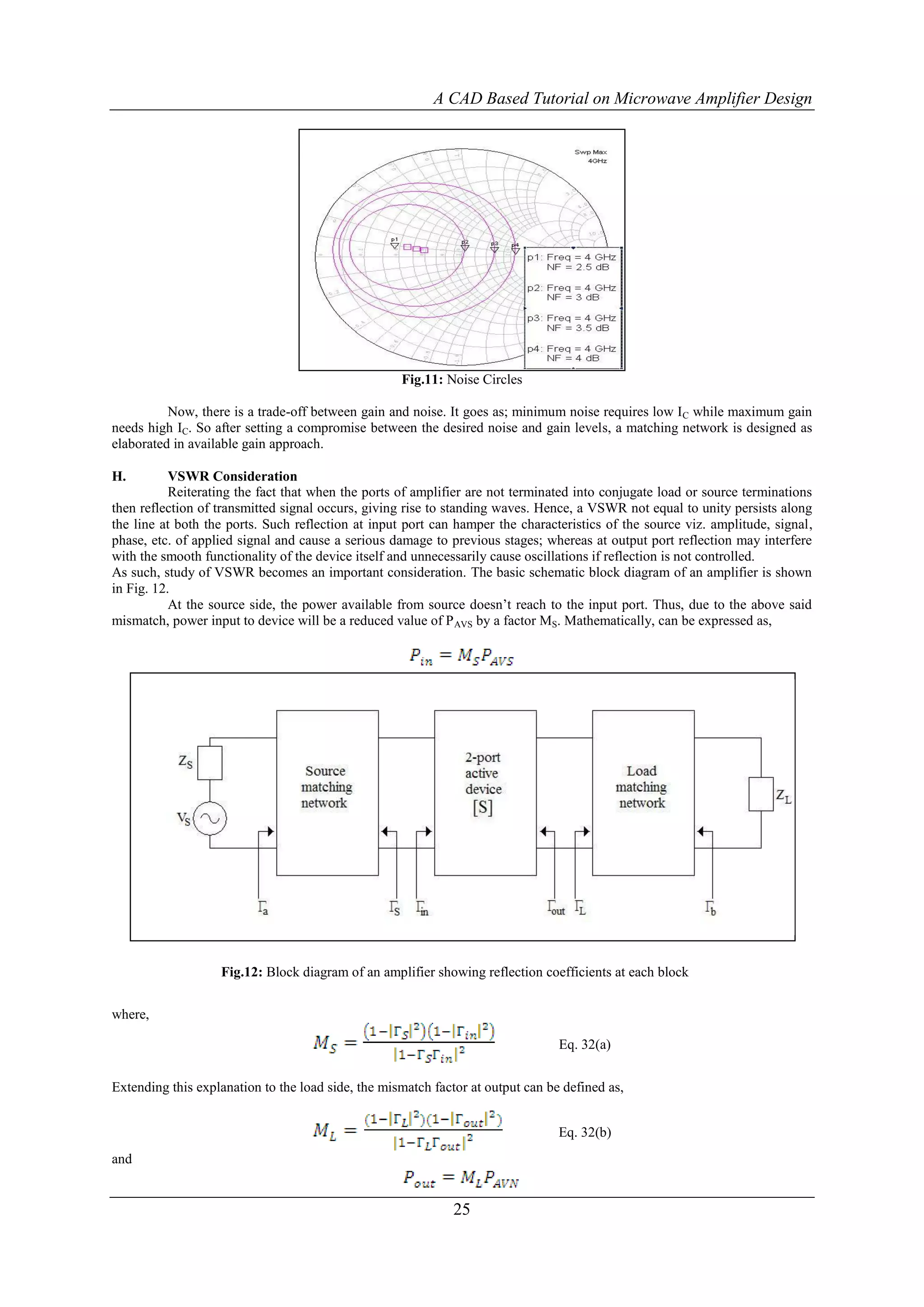
The VSWR corresponding to these reflections from source and load matching networks are,
Eq. 35(a)
Eq. 35(b)
VSWR will be unity when and are zero, or when ΓS=Γin* and ΓL=Γout* i.e. the case of conjugate matched loads.
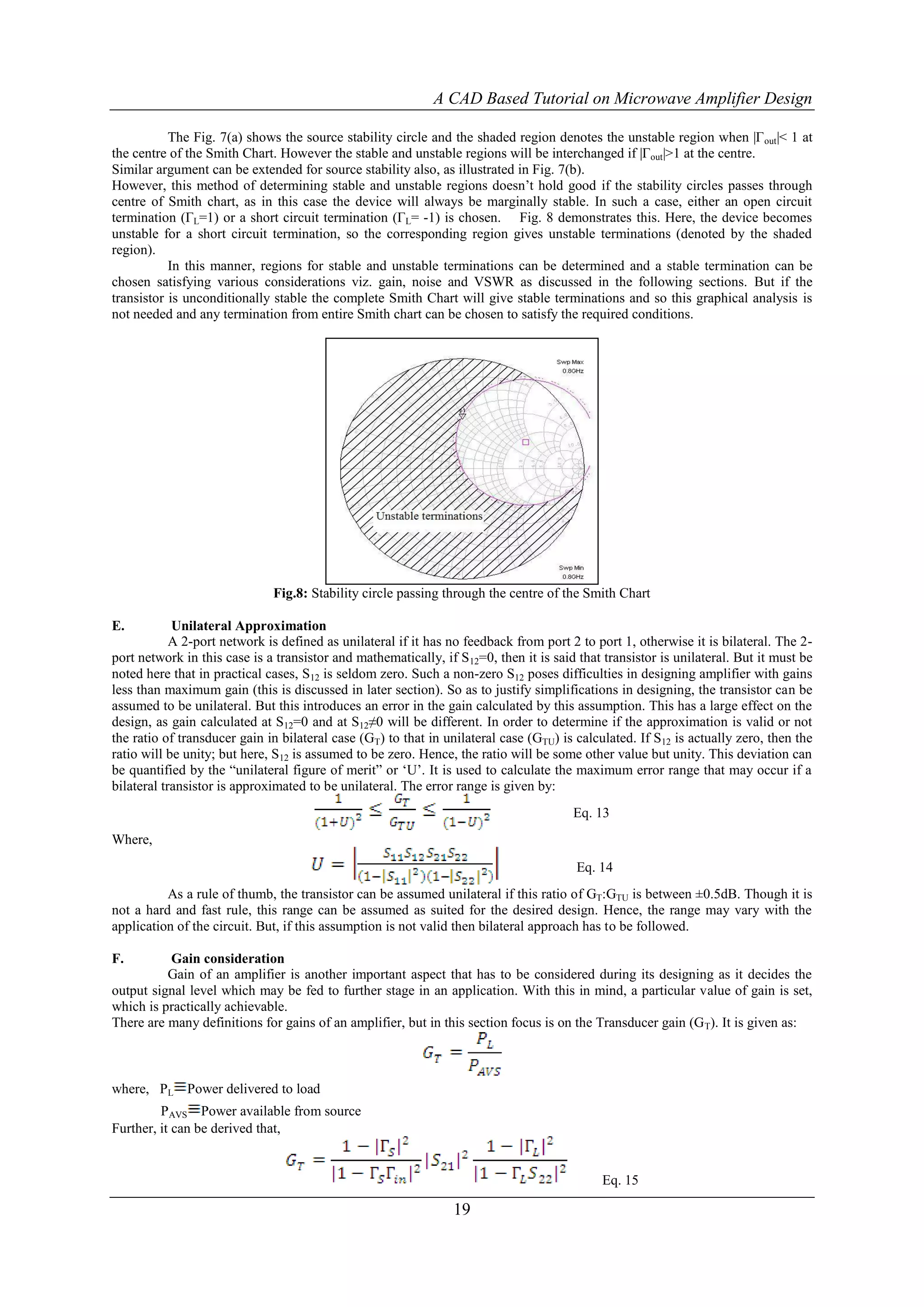
I. Selection of matching network topology
The need for matching network has already been discussed in previous sections as in to achieve required level of
gain, noise, power transfer, etc. Such a matching network can be designed using either transmission line or lumped elements.
But practically in most cases transmission lines are used; microstrip lines to be more precise. A single stub matching can be
used for the design. However, to reduce the transition interaction between the line and stub, balanced stub matching can be
employed. But, if lumped element matching technique is used, then the preferred circuit is shown in Fig. 13, so that DC
biasing becomes easy by adding a DC source in series with inductor. Also it acts as a High Pass Filter and blocks the low
frequency baseband signals which can cause oscillations due to an inherent high gain of the device at lower frequencies.
Fig.13: An example of matching network
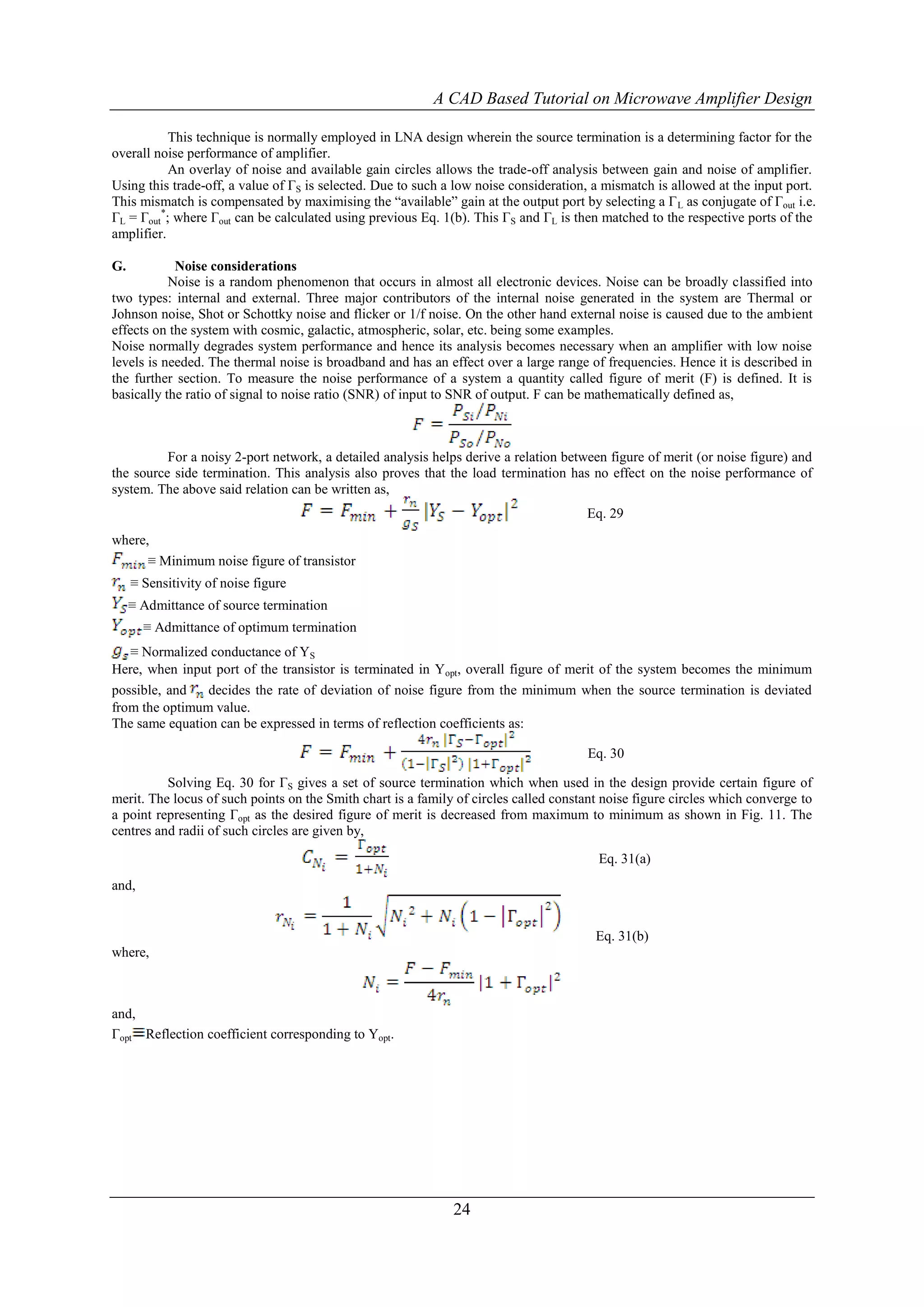
III. CONCLUSION
The above discussion provides a lucid understanding of the procedure for amplifier design. However, the
techniques discussed here are exclusively applicable only to narrowband amplifier because of following reasons; S-
parameters are frequency dependent and gain is higher at low frequency than at higher frequency. Also, the matching
networks hold good for barely an octave as the passive elements here are largely dependent on frequency.
REFERENCES
[1]. Vendelin, G. D., Pavio, A. M., Rohde, U. L., Microwave Circuit Design Using Linear And Nonlinear Techniques,
(2nd Edition), (John Wiley & Sons Publications, Inc., Hoboken, New Jersey.)
[2]. Gonzalez, G., Microwave Transistor Amplifiers: Analysis And Design, (2nd Edition), (Prentice Hall Publications,
Inc., Upper Saddle River, New Jersey.)
[3]. Pozar, D. M., Microwave Engineering, (2nd Edition), (John Wiley & Sons Publications, Inc., Hoboken, New
Jersey.)
[4]. Liao, S. Y., Microwave Circuit Analysis and Amplifier Design, (1st Edition), (Prentice Hall Publications, Inc.,
Upper Saddle River, New Jersey.)
26