Download to read offline

![4
1–|S11|2
–|S22|2
+|∆|2
2|S12 S21|
≥1K =
|∆|=|S11 S22 – S21 S12|< 1
B1
=1+|S11 |2
– |S22|2
–|∆|2
> 0
B2
=1+|S22|2
– |S11|2
–|∆|2
> 0
ΓS ΓLΓIN ΓOUT
ΓS ΓL
[S]
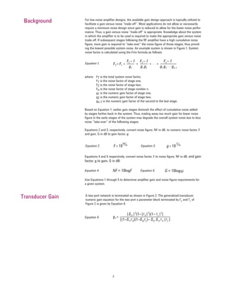
The s-parameters describe a device for a particular set of conditions, such as frequency,
bias, and temperature as shown in Equation 6. Transducer gain, gT
, is a function of the
s-parameters, ΓS
, and ΓL
. Convert numeric transducer gain gT
, to gain GT
in dB by use of
Equation 5. When the device is terminated in the same impedance as when s-parameters
were measured, ΓS
and ΓL
are zero and gT
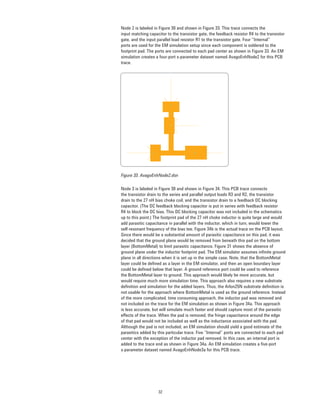
= |S21
|2
.
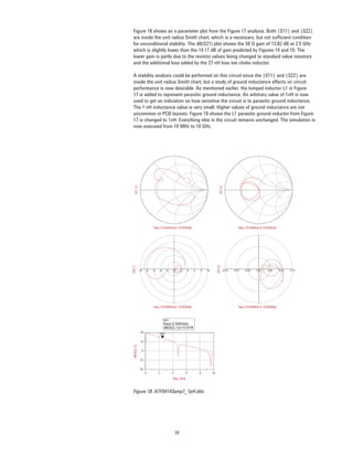
The Figure 2 two-port network may be stable or potentially unstable. It is imperative that
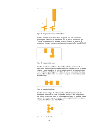
the amplifier does not oscillate in the product environment, since such behavior leads to
product malfunction. If the two-port is potentially unstable, there are conditions where
oscillations can occur. Certain source or load terminations that produce the oscillations
provide the conditions necessary for the unstable behavior. This type of design is called a
conditionally stable design. If the conditionally stable design method is utilized, extreme
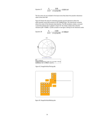
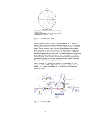
care must be observed to guarantee that a source or load termination that produces an
oscillation is never presented to the amplifier. This applies to all frequencies in-band and
out-of-band. This can be a difficult task at best in most applications. The unconditionally
stable design approach allows any source or load terminations, which have reflection
coefficient magnitudes between 0 and 1, inclusive, presented to the amplifier without
the possibility of an oscillation. It is highly recommended that the two-port is made
unconditionally stable at all frequencies. An unconditionally stable design guards against
unexpected oscillations, which cause product malfunction.
Two-port stability is analyzed using stability circles or equations. In this design
example, stability equations are used to achieve an unconditionally stable design at all
frequencies. The stability equations are a function of the Figure 2 two-port s-parameters.
Equation 7 gives the value for stability factor K, which is made greater than or equal to
unity for stability. Additionally, stability factors ∆, B1, and B2 are shown by Equations
8, 9, and 10 respectively. To achieve unconditional stability, the two-port must satisfy
Equation 7 and either Equation 8, 9, or 10. If Equation 8, 9, or 10 is satisfied, all three
equations are, by definition, satisfied. Thus, if K ≥ 1, the two-port network may not be
unconditionally stable. Having K ≥ 1 is a necessary, but not sufficient, condition for
unconditional stability. Additionally, Equation 8, 9, or 10 is analyzed to determine if the
two-port network stability is unconditional. Thus, |∆| < 1, or B1 > 0, or B2 > 0 must also
be met along with K ≥ 1 to guarantee unconditional stability.
Figure 2.
Stability Analysis
Equation 7.
Equation 8.
Equation 9.
Equation 10.](https://image.slidesharecdn.com/1-150921033203-lva1-app6892/85/1-vip-agilent-3-4-320.jpg)
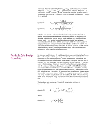
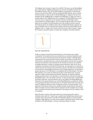
![6
Substituting Equation 14 into Equation 15 yields the available gain equation, gA
, as shown
in Equation 16, which is a function of ΓS
and the two-port s-parameters.
gA =
1–|ΓS|2
1
|1–S11ΓS|2
1–|ΓOUT|2|S21|2
Equation 15.
gA =
|S21|2
(1–|ΓS|2
)
S22 – ∆ΓS
1– S11ΓS
1– |1– S11ΓS|2
( (
2
Equation 16.
Equation 21 describes transistor noise factor performance. As shown in this equation,
transistor noise performance is independent of load termination and is determined solely
by its source termination and noise parameters. The noise parameters fully describe the
noise performance of a device for a specific set of conditions such as frequency, bias,
and temperature.
F= FMin
+
4rn|ΓS – Γopt|2
(1–|ΓS|2
)|1 + Γopt|2Equation 21.
Noise Figure Design
Procedure
When the device output is conjugately matched for a given source termination ΓS
,
then transducer gain, gT
, is simplified in terms of the s-parameters and ΓS
. Conjugately
matching the output mathematically yields ΓL
= ΓOUT
* and Equation 15 yields available
gain, gA
:
A family of circles known as available gain circles are constructed that provide a
specific amount of mismatch at the device input. An infinite number of source
terminations forming the circle allow selection of mismatch at the device input. To
construct an available gain circle, locate the center of the circle on a Smith chart and
draw the circumference from a calculated radius. Locate the center for a particular gain
circle using Equation 20, which yields a magnitude and angle. The desired available gain
in dB is converted to numeric gain factor gA
for Equation 17. Equation 17 is then used in
Equations 19 and 20.
ga =
gA
|S21|2
Equation 17.
C1
= S11 – ∆S*22
Equation 18.
Ra =
[1– 2K|S12 S21|ga
+|S12 S21|2
g2
a]½
1 + ga(|S11|2
– |∆|2
)
Equation 19.
Plotting available gain circles in conjunction with noise contours allows an easy
selection of gain versus noise figure for the amplifier.
Ca =
ga
C1
*
1 + ga(|S11|2
– |∆|2
)
Equation 20.
The radius of an available gain circle is calculated by equation 19:
Transistor noise factor F is a function of ΓS
, FMin
, rn
, and Γopt
, where FMin
, rn
, and Γopt
are known
as the transistor noise parameters. ΓS
terminates the two-port input of Figure 2. As ΓS
approaches Γopt
, the transistor noise factor approaches its minimum. As ΓS
departs from
Γopt
, the noise factor increases from its minimum value. The rate at which the noise factor
increases depends on the noise resistance rn
. Conversion of transistor noise factor to noise
figure in dB is obtained from Equation 4. Equation 22 obtains the noise resistance rn if FMin
,
Γopt
, and the noise factor with the input terminated in 50 Ω is known. (ΓS
= 0)](https://image.slidesharecdn.com/1-150921033203-lva1-app6892/85/1-vip-agilent-3-6-320.jpg)
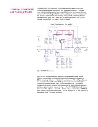
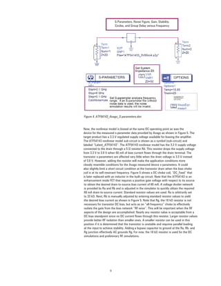
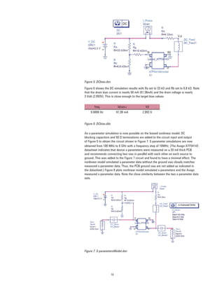
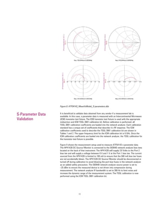
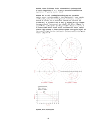
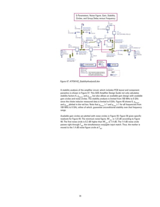

This document describes a method for designing a low noise RF amplifier for a 802.11b receiver application using Agilent's ADS design tools. The design procedure uses available gain and stability analysis to create an unconditionally stable amplifier circuit that minimizes noise and meets specifications. Key steps include analyzing the transistor's S-parameters, performing an EM simulation of the printed circuit board layout, and comparing the simulation and measurement results to verify the design meets requirements.


![射頻電子 - [第六章] 低雜訊放大器設計](https://cdn.slidesharecdn.com/ss_thumbnails/ch6-150613065106-lva1-app6892-thumbnail.jpg?width=640&height=640&fit=bounds)


![Agilent ADS 模擬手冊 [實習2] 放大器設計](https://cdn.slidesharecdn.com/ss_thumbnails/2adsamp-150613072818-lva1-app6892-thumbnail.jpg?width=640&height=640&fit=bounds)
![Multiband Transceivers - [Chapter 2] Noises and Linearities](https://cdn.slidesharecdn.com/ss_thumbnails/ch2-150613070933-lva1-app6892-thumbnail.jpg?width=640&height=640&fit=bounds)

![RF Circuit Design - [Ch4-1] Microwave Transistor Amplifier](https://cdn.slidesharecdn.com/ss_thumbnails/ch4-1-150613064409-lva1-app6892-thumbnail.jpg?width=640&height=640&fit=bounds)


![Chapter 2 [compatibility mode]](https://cdn.slidesharecdn.com/ss_thumbnails/chapter2compatibilitymode-150427213042-conversion-gate01-thumbnail.jpg?width=640&height=640&fit=bounds)


![[Links vip.net] gap fill reading practice](https://cdn.slidesharecdn.com/ss_thumbnails/linksvip-150924023536-lva1-app6891-thumbnail.jpg?width=640&height=640&fit=bounds)
![Chapter 4 internetworking [compatibility mode]](https://cdn.slidesharecdn.com/ss_thumbnails/chapter4-internetworkingcompatibilitymode-150427213051-conversion-gate02-thumbnail.jpg?width=640&height=640&fit=bounds)


![Chapter3 [compatibility mode]](https://cdn.slidesharecdn.com/ss_thumbnails/chapter3compatibilitymode-150427213056-conversion-gate01-thumbnail.jpg?width=640&height=640&fit=bounds)
![Mang may tinh [compatibility mode]](https://cdn.slidesharecdn.com/ss_thumbnails/mangmaytinhcompatibilitymode-150427213100-conversion-gate01-thumbnail.jpg?width=640&height=640&fit=bounds)

![Chapter1 [compatibility mode]](https://cdn.slidesharecdn.com/ss_thumbnails/chapter1compatibilitymode-150427213055-conversion-gate01-thumbnail.jpg?width=640&height=640&fit=bounds)


