M-Solv is a company that designs and sells manufacturing equipment combining high-precision motion control with laser patterning, inkjet printing, and spray deposition technologies. They presented on using these technologies for large-area electronics manufacturing. Specifically, they discussed using inkjet printing and laser processing to digitally manufacture capacitive touch sensors and for a new "one step interconnect" process for thin-film photovoltaics that deposits all layers and connections in a single pass, reducing costs. Funding from Innovate UK and the EU is acknowledged.
A durable and flexible display with low-power consumption, high-contrast ratio, has been a technical challenge for years. They have to be lightweight, rugged, and in some cases, conformal, wearable, rollable and unbreakable. The recent successful integration of flexible display technologies and the traditional web-based processing and/or inkjet technologies has opened up the possibility of low cost and high throughput roll-to-roll manufacturing and has shown the potential to replace the paper used today.
A durable and flexible display with low-power consumption, high-contrast ratio, has been a technical challenge for years. They have to be lightweight, rugged, and in some cases, conformal, wearable, rollable and unbreakable. The recent successful integration of flexible display technologies and the traditional web-based processing and/or inkjet technologies has opened up the possibility of low cost and high throughput roll-to-roll manufacturing and has shown the potential to replace the paper used today.
Feasibility Of Graphene Inks In Printed Electronics V5Vishnu Chundi
Presentation delivered at the International Conference on Nanoscience and Technology,India, January,2012. Evaluating the technical and commercial aspects of using graphene inks for printed electronics applications. Suggested a road-map for the future applications. Touches upon the competing technologies for ITO replacement. Performed SWOT analysis of graphene inks
This is a technical review for electrical and mechanical engineers and project managers involved in designing your next-generation products. We will cover the two processes for producing 3-dimensional molded interconnects; Double-Shot molding and Laser Direct Structuring, with an emphasis on laser direct structuring.
Presented for TTI Vanguard "Shift Happens" conference (http://bit.ly/TTIVshifthappens) visit to PARC, this is an overview of an all-printed and therefore low-cost, disposable sensor that conforms to the curvature of a helmet.
Developed for DARPA to monitor soldiers' blast exposure and prevent traumatic brain injury, the technology can be applied to multiple biomedical and other applications.
Howto intall and operate eva vacuum glass laminating machinery and make lamin...Eva Glass
eva vacuum glass laminating machine installation and operation howto guide, and notes of manufacture safety laminated glass with eva interlayer film by silicone vacuum bag method
application and advantages of printed electronics.
Revolutionary technique of making electronics
components
•Printed electronics is based on new materials
and manufacturing processes.
•Simple way of fabrication of simple electronics
components
These slides use concepts from my (Jeff Funk) class to analyze the near-term future for touch-screen displays. Improvements in durability, sensitivity, and flexibility are being implemented
Atomic Layer Deposition solutions for SiC Power ElectronicsBeneq
Power Electronics International
Brussels, Belgium
19.04.2023
Atomic Layer Deposition solutions for SiC Power Electronics
Integrated ALD passivation/gate dielectric stack for SiC MOSFET
Presented by Mikko Söderlund from Beneq Oy
High Capacity Planar Supercapacitors and Lithium-Ion Batteries by Modular Man...Bing Hsieh
High Capacity Planar Supercapacitors and Lithium Ion Batteries by Modular Manufacturing
Novel planar supercapacitors (SC) and lithium ion batteries (LIB) having interdigitated electrodes for large format applications will be presented. We will discuss the design principles of the new planar structures, their potential to give > 5X improvement in capacity over current supercapacitors, their pack designs, as well as low cost fabrication by modular manufacturing. The drawings given in the following link depict the plan view (top) and the cross-sectional view (bottom) of a planar LIB, wherein the dotted and the hatched areas are the positive and the negative electrodes respectively; the gray areas are the current collectors and the gray lines are the grid lines. Unlike the known interdigitated thin film microsupercapacitor design where the current collectors are situated on the top or bottom surfaces of the electrodes and paralleled to the plane of the substrate and can only exert limited weak fringe fields, the current collectors in our new design are running along the sidewalls of the electrodes and are perpendicular to the substrate and can thus provide strong direct fields, as indicated by the purple arrow, to promote facile ion movement across the entire thickness of the electrodes (20-100 µm). In addition, the relatively narrow inter-spaces between two opposite electrodes (20-100 µm) may allow much higher power densities than ever. Due to their scalability and low cost modular manufacturing processes by printing, the new planar SC/LIB may be designed for a wide range of applications such as mobile devices, transportation, and grid and distributed energy storage.
https://drive.google.com/file/d/0B7fDeNQTYRc9VDdOTTVYRmh2QWc/view?usp=sharing
3. CLICK TO EDIT MASTER TITLE STYLE
3
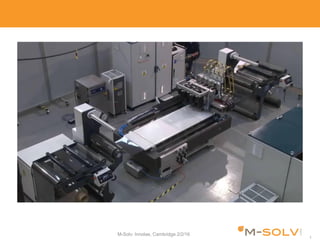
M-Solv: Innolae, Cambridge 2/2/16
M-SOLV: WHO WE ARE
• Design, build and sell manufacturing equipment for
R&D and high volume production.
• Combining high performance motion control
platforms with innovative process technologies:
- Laser patterning/micromachining, ink jet of functional
materials, and spray deposition of solution based
materials.
• Developing low energy, low cost of ownership and
environmentally friendly manufacturing processes
using the latest cutting edge technologies.
• Manufacture robust capacitive touch sensors for
industrial applications with Touchnetix
4. CLICK TO EDIT MASTER TITLE STYLE
4
M-Solv: Innolae, Cambridge 2/2/16
WHO WE ARE : Locations
CN Innovations
Parent Company
Hong Kong
Anderson Group
Manufacturing Partner
Taiwan
M-Solv HK
Hong Kong
M-Solv Limited
United Kingdom
5. 5
M-Solv: Innolae, Cambridge 2/2/16
Introduction
• Large area electronic devices we can make
with inkjet and laser:
• Touch sensor
• Thin-film PV interconnect
• What else?
11. 11
M-Solv: Innolae, Cambridge 2/2/16
Digital manufacture
• Minimise materials waste
• Optimise throughput
• This is a strong driver for the digital
process
• 1-11 are different sensors
represented by multi-layer CAD
files, layers for:
• Metal print
• Metal laser
• ITO laser
• Overcoat print
13. 13
M-Solv: Innolae, Cambridge 2/2/16
Copper vs silver
• Copper is lower cost than silver
• Electromigration is a big problem
with silver (for M-Solv anyway)
• Our offering is ultra-robust
sensors
• Copper is much less prone to EM
• Copper is much more difficult to
sinter
• Can’t use oven – oxidation
• Laser works very well
14. CLICK TO EDIT MASTER TITLE STYLE
14
M-Solv: Innolae, Cambridge 2/2/16
Conclusions on capacitive touch
• Inkjet + laser is an ideal way of depositing metallisation
• Fast and efficient
• Print resolution not really OK
- Laser defines high resolution tracks down to 25mm/25mm track/gap
- Need a laser anyway to pattern the ITO electrodes
• Copper is resistant to electromigration
• Fully digital
- Inkjet and laser run direct from CAD
- Ideal for niche products with limited production runs
- Digitally-generated mixed product substrates minimise wastage and are key to good
margins!
15. CLICK TO EDIT MASTER TITLE STYLE
15
M-Solv: Innolae, Cambridge 2/2/16
Conventional thin-film Interconnect
• Thin Film PV is made by mainly vacuum deposition of a
TCO/semiconductor/metal stack, a few mm thick on, usually, a glass
substrate. The ~ 1m2 panels are divided into series interconnected cells
by laser scribing across the panel after each layer is deposited.
Three main inorganic TF PV materials:
• Thin-film silicon (TF-Si)
• Cadmium telluride (CdTe)
• CIGS/CIS
16. CLICK TO EDIT MASTER TITLE STYLE
16
M-Solv: Innolae, Cambridge 2/2/16
Conventional process
• Disadvantage:
- The laser processes, P1, P2, P3, happen at room temperature in air,
the deposition processes happen at high temperature in vacuum –
air/vacuum/air transitions can only occur at room temperature
P1
P2
P3
TCO
CdTe
metal
P1, P2 and P3 are laser processes
that happen after the TCO, CdTe
and metal deposition steps,
respectively
17. CLICK TO EDIT MASTER TITLE STYLE
17
M-Solv: Innolae, Cambridge 2/2/16
Conventional process
• As the TCO-coated glass panel goes along the automated production line
it goes repeatedly from air to vacuum and gets heated and cooled for the
various processes until it finally emerges as a complete module ready for
lamination
0
100
200
300
400
500
Temperature(°C)
Panel Transit time
Laser P1 CdS CdTe Activation Laser P2
Back
contact
Laser P3
TCO
Glass
δt = 1500°c
Ambient Vacuum
18. CLICK TO EDIT MASTER TITLE STYLE
18
M-Solv: Innolae, Cambridge 2/2/16
One Step Interconnect (OSI) process
• After full stack deposition, depth-controlled laser scribes are made A, B,
P3. A is filled with UV-cured insulating inkjet material, B is filled by inkjet
with metal which bridges A making the interconnect. This all happens in a
single pass of the process heads! Fast & self aligning.
TCO
CdTe
Metal
A B P3
19. CLICK TO EDIT MASTER TITLE STYLE
19
M-Solv: Innolae, Cambridge 2/2/16
One Step Interconnect (OSI) process
• Using OSI there is only one ambient-vacuum and one vacuum-ambient
transition. The process is shorter in time and length of the production line.
The temperature profile is flatter – total DT reduced by 400⁰C. This should
facilitate better process control
0
100
200
300
400
500
Temperature(°C)
Panel Transit time
CdS CdTe Activation
Back
contact
OSI
TCO
glass
ΔT = 1100°C
ambient vacuum
20. CLICK TO EDIT MASTER TITLE STYLE
20
M-Solv: Innolae, Cambridge 2/2/16
Example CdTe minimodule: Laser
21. CLICK TO EDIT MASTER TITLE STYLE
21
M-Solv: Innolae, Cambridge 2/2/16
Insulator
22. CLICK TO EDIT MASTER TITLE STYLE
22
M-Solv: Innolae, Cambridge 2/2/16
Conductor
23. CLICK TO EDIT MASTER TITLE STYLE
23
M-Solv: Innolae, Cambridge 2/2/16
Cell measurement
• Measure the J/V curve of a cell under AM1.5 illumination, using the OSI interconnect to
access the front electrode. In the equivalent circuit – the interconnect does not add
significant series resistance Riser or add a low Rish . This is shown by the good fill factors in
the J/V curves on the following slides.
Incident Light
24. CLICK TO EDIT MASTER TITLE STYLE
24
M-Solv: Innolae, Cambridge 2/2/16
J/V: cell strings
• Interconnect performance is good, a string of 5 cells was probed as 1,2,…,5 cell substrings
and the J/V curves are plotted below, with fill-factors indicated. Efficiency of the mini-
module was ~11% as expected from reference cell measurements.
25. 25
M-Solv: Innolae, Cambridge 2/2/16
Laser sintering on sensitive PV material (CIGS)
All copper grid
All copper
mini-module
This is tricky because direct exposure to the laser beam destroys the
CIGS and the copper is printed on 3 substrates, metal, polymer
dielectrtric and TCO – all need a different cure dose.
IV curve: just as good as Ag + oven
26. CLICK TO EDIT MASTER TITLE STYLE
26
M-Solv: Innolae, Cambridge 2/2/16
OSI: One Step Interconnect
• Separate thin film deposition from interconnect
• Suitable for all thin film PV technologies CIGS, CdTe, TF-Si, etc
• Suitable for roll-to-roll processing
• Deposit all layers in thin film PV stack – no need to break vacuum
• OSI divides and interconnects in a single process:
- Depth controlled laser scribes
- Inkjet insulator and metal
• Interconnects are good
• Process is fast and cost effective
• Opens up many new possibilities in thin film PV manufacturing
• Efficiency up Cost down!
27. CLICK TO EDIT MASTER TITLE STYLE
27
M-Solv: Innolae, Cambridge 2/2/16
SMI: Scanned mask imaging
• Process able to match performance of
excimer laser systems with a solid state
laser
- <5 µm resolution, high throughput
Multi Mode Solid State Laser
Low Average Power <100W
Low Pulse Energy to few mJ
Repetition rate approximately 10 kHz
Top Hat Profile
Low Running Costs
• Applications:
- Semiconductor packaging
- Micro-machining
- ITO Patterning
28. CLICK TO EDIT MASTER TITLE STYLE
28
M-Solv: Innolae, Cambridge 2/2/16
SMI: scanned mask imaging
30. CLICK TO EDIT MASTER TITLE STYLE
30
M-Solv: Innolae, Cambridge 2/2/16
Summary and acknowledgements
• Presented inkjet printing for two large-area electronics applications
- Digital capacitive touch sensor manufacturing
- One step thin-film PV interconnection
• Indicated how laser processing complements inkjet deposition
• Funding by Innovate UK and the EU H2020 programme is gratefully acknowledged
adam.brunton@m-solv.com